EP0483436A1 - Taktfrequenztester - Google Patents
Taktfrequenztester Download PDFInfo
- Publication number
- EP0483436A1 EP0483436A1 EP90480172A EP90480172A EP0483436A1 EP 0483436 A1 EP0483436 A1 EP 0483436A1 EP 90480172 A EP90480172 A EP 90480172A EP 90480172 A EP90480172 A EP 90480172A EP 0483436 A1 EP0483436 A1 EP 0483436A1
- Authority
- EP
- European Patent Office
- Prior art keywords
- input
- nand gate
- output
- frequency
- clock
- Prior art date
- Legal status (The legal status is an assumption and is not a legal conclusion. Google has not performed a legal analysis and makes no representation as to the accuracy of the status listed.)
- Withdrawn
Links
- 230000001960 triggered effect Effects 0.000 claims description 9
- 238000010586 diagram Methods 0.000 description 6
- 230000007704 transition Effects 0.000 description 4
- 238000004891 communication Methods 0.000 description 3
- 238000012360 testing method Methods 0.000 description 3
- 230000005540 biological transmission Effects 0.000 description 1
- 230000007423 decrease Effects 0.000 description 1
- 238000005516 engineering process Methods 0.000 description 1
Images


Classifications
-
- H—ELECTRICITY
- H03—ELECTRONIC CIRCUITRY
- H03K—PULSE TECHNIQUE
- H03K5/00—Manipulating of pulses not covered by one of the other main groups of this subclass
- H03K5/22—Circuits having more than one input and one output for comparing pulses or pulse trains with each other according to input signal characteristics, e.g. slope, integral
- H03K5/26—Circuits having more than one input and one output for comparing pulses or pulse trains with each other according to input signal characteristics, e.g. slope, integral the characteristic being duration, interval, position, frequency, or sequence
-
- G—PHYSICS
- G01—MEASURING; TESTING
- G01R—MEASURING ELECTRIC VARIABLES; MEASURING MAGNETIC VARIABLES
- G01R23/00—Arrangements for measuring frequencies; Arrangements for analysing frequency spectra
- G01R23/02—Arrangements for measuring frequency, e.g. pulse repetition rate; Arrangements for measuring period of current or voltage
- G01R23/15—Indicating that frequency of pulses is either above or below a predetermined value or within or outside a predetermined range of values, by making use of non-linear or digital elements (indicating that pulse width is above or below a certain limit)
Definitions
- This invention relates to timing arrangement circuits for electronic systems and more particularly to devices for testing the characteristics of a clock.
- Devices for testing the timing arrangement circuits and more particularly the characteristics of the clocks provided by the latter circuits are of general interest in the data processing and communication fields.
- the general tendency is to improve the performance of the systems and to increase their speed, thus entailing the electronic components therein included be clocked at higher and higher speeds.
- the latter components are consequently used in a frequency range which is ever more close to their critical frequency limit, over which a disfunction of the latter is likely to appear.
- the clocks which are used to drive the electronic components included into a data processing system should therefore be closely checked in order to make sure that the electronic components are driven at a desired frequency range.
- the technology of DRAM requires that a dynamic Random Access Memory be regularly refreshed in order to save its contents. In that case, the refreshing frequency should be checked to be inferior to the critical refreshing frequency of the DRAM, value under which the contents of a DRAM might unfortunately be destroyed.
- the clock frequency tester which indicates whether the frequency of a clock (FB) has a value which is comprised within a predetermined range of values (FA-FA/n, FA+FA/N) around a reference frequency value (FA) of a reference clock.
- the frequency tester further includes a phase frequency comparator which has a first and second input lead F1 and F2 which is respectively connected to the output of the divide-by-n circuit and to the output of the frequency mixer.
- the phase frequency comparator generates an output signal which remains at a steady level whenever F1 input signal has a frequency value which is superior to that of the F2 input signal, that is to say when the FB frequency to be tested is comprised within the range of values (FA-FA/n, FA+FA/n). Since the factor n of the division can be easily adjusted, any desired degree of accuracy can be provided by the frequency tester of the invention.
- the frequency mixer is a D-latch which has a clock-input connected to the FA reference clock and a D-input connected to the clock to be tested.
- the frequency tester further includes a second (resp. a third phase frequency comparator) which has two input leads F'1 and F'2 (resp. F''1 and F''2) respectively receiving FA/2 and FB/3 (resp. FB and FA/2) and which provides a steady output signal whenever the frequency value of its former input F'1 (resp. F''1) is superior to that of the latter input F'2 (resp. F''2) that is to say whenever the ratio FB/FA is inferior to 1.5 (resp. is superior to 0.5).
- a second resp. a third phase frequency comparator
- every phase frequency comparator is combined in such a way as to provide an output signal QT which remains at a steady level whenever the FB/FA ratio is comprised within the range (1-1/n, 1+1/n) for FB varying from zero to the infinite.
- FIG. 1 illustrates the preferred embodiment of the invention.
- Figure 2 details a negative edge triggered phase frequency comparator which is used in the preferred embodiment of the invention.
- Figure 3 details a positive edge triggered phase frequency comparator which is used in the preferred embodiment of the invention.
- Figure 4 details a divide-by-3 circuit which is used in the preferred embodiment of the invention.
- Figure 5 shows a diagram illustrating the evolution of the output frequency of frequency mixer 100 with the ratio FB/FA.
- Figure 6a details timing diagrams illustrating the operating of phase frequency comparator 102.
- Figure 6b shows a diagram illustrating the evolution of the output frequency of comparator 102 with the ratio FB/FA.
- Figure 6c shows a diagram illustrating the evolution of the output frequency Qt of AND gate 113 with the ratio FB/FA.
- Figure 7 and 8 show typical timings illustrating how operates the frequency tester according of the present invention.
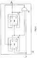
- the clock frequency tester includes a D-latch 100 which is used as a digital frequency mixer, that is to say receives the reference clock FA at its clock input and also receives the clock FB which is to be tested at its D-input lead.
- the reference clock FA is also transmitted to the input of a divide-by-n circuit 101, the output of which being connected to a F1 input lead 114 of a phase frequency comparator 102.
- Phase frequency comparator 102 has a second input lead F2 which is connected to the Q output of D-latch 100, lead 110.
- Fa clock is also transmitted to a divide-by-2 circuit 105, the output of which being connected to a F'1 input lead of a second phase frequency comparator 103 and to a F''2 input lead of a third phase frequency comparator 104.
- FB clock is transmitted to the input of a divide-by-3 circuit 106 and to a F''1 input lead of the phase frequency comparator 104.
- the output of divide-by-3 circuit 106 is connected to a F'2 input lead of phase frequency comparator 103.
- the Q2, Q'2 and Q'2 output of respectively phase frequency comparator 102, 103 and 104 are connected each one to an input lead of an AND gate 108, the output of which carrying a QT signal on lead 113.
- QT signal is representative of the FB/FA ratio and more particularly indicates whether the tested frequency FB has a value which is comprised within the range ( FA - FA/n ; FA + FA/n ) where n is the factor of division of divide-by-n circuit 101.
- Phase frequency comparator 102 (or 103, or 104) includes a set of 4 Set-Reset flip-flops 200-201, 202-203, 204-205 and 207-208 and a 4-input-NAND gate 206, the output of which being connected to the reset input of every Set-Reset flip-flop. More accurately, the F1 signal (resp.
- NAND 202 has a second input which is connected to the output of NAND 203.
- NAND 204 has a second input which is connected to the output of NAND 205, to a third input of NAND 206 and to a first input of NAND 207.
- NAND 204 has an output which is connected to a first input of NAND 205, a second input of which being connected to a fourth input of NAND 206, to a second input of NAND 207 and to the output of NAND 208.
- NAND 207 has a third input which is connected to the output of NAND 206 and an output which is connected to a first input of NAND 208.
- F2 signal (or F'2 for comparator 103, or F''2 for comparator 104) is transmitted to a second input of NAND 208.
- NAND gate 201 and NAND gate 207 respectively provides a Q1 and Q2 signal which are representative of the F1/F2 ratio. More accurately, whenever F2 is superior to F1, the output Q1 of NAND gate 201 remains at a high level while the output Q2 of NAND gate 207 is characterized by the existence of transitions. Conversely, whenever F1 is superior to F2, the output Q2 of NAND gate 207 remains at a high level while the output Q1 of NAND gate 201 is characterized by the existence of transitions.
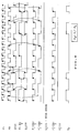
- Figure 6A shows typical timings of the F1, F2, Q1 and Q2 illustrating the operating of negative edge triggered phase frequency comparator 102.
- FIG. 6b there is shown a diagram illustrating the evolution of the Q2 output signal when the FB/FA ratio varies. Because of the existence of D-latch 100 and divide-by-n circuit 101, the Q2 signal at the output of phase frequency comparator 102 remains at a high state when the ratio FB/FA is comprised in the following value ranges: (0, 1/n) ; (1-1/n, 1+1/n) ; (2-1/n, 2+1/n) ; (3-1/n, 3+1/n) ; etc...
- Divide-by-2 circuit 105 and divide-by-3 circuit 106 respectively provide a F'1 and F'2 signals which are transmitted to the two inputs of a second phase frequency comparator 103.
- the Q'2 output of the latter comparator therefore provides a steady high state whenever the FB/FA ratio is inferior to 1.5
- the output of divide-by-2 circuit 105 is also connected to a F''1 input of a third phase frequency comparator 104, the F''2 input of which being connected to the tested FB clock.
- the Q''2 output of the third phase frequency comparator 104 therefore provides a steady high state whenever the FB/FA ratio is superior to 0.5.
- AND gate 108 which have three input leads respectively connected to the Q2, Q'2 and Q''2 output of comparators 102, 103 and 104, provides a QT signal on lead 113 which indicates whether the tested clock signal Fb is such that the FB/FA ratio is comprised within the range (1-1/n, 1+1/n).
- FIG 6c there is shown a diagram illustrating the evolution of Qt output of AND gate 108 when the ratio FB/FA varies.
- the QT signal remains at a steady high level whenever the latter ratio remains within the determined range of values.
- the FB frequency decreases or increases with respect to the reference Fa frequency
- transitions appear on the QT signal and consequently indicates a disfunction of the FB clock generator.
- the occurrence of that disfunction can easily be detected by storing the occurrence of a low state in QT signal in an appropriate (not shown in the figure) latch.
- the range (1-1/n, 1+1/n) can be easily adapted and adjusted simply by changing the factor of division of divide-by-n circuit 101, thereby providing a very simple but accurate frequency tester.
- Figures 7 and 8 show typical timings illustrating how operates the frequency tester according to the present invention with a divide-by-4 circuit 101. Consequently the tester according to the present invention indicates by the existence of a steady high level at the output lead 113 of AND gate 108 whether the FB/FA ratio is comprised within the range (0,75; 1,25).
- Figure 7 particularly shows timings for a FB/FA ratio of 0,8 , that is to say for a value which is comprised within the preceding range (0,75; 1,25).
- QT output signal on lead 113 remains at a steady high level state.
- figure 8 shows the corresponding timings for a FB/FA ratio of 0,7 , that is to say for a value which is not comprised within the range (0,75; 1,25).
- QT output lead 113 is characterized by the existence of transitions which are used in order to reset a (not shown) latch, the low level of which indicating a disfunction in the clock generators.
- Phase frequency comparator 102 includes a set of two D-latches 301 and 302 having their clock input respectively connected to F1 and F2 signals and their D-input connected to the positive voltage source V+.
- the Q output of D-latch 301 is connected to a first input of NAND gate 304 and to a first input of NAND 305.
- the Q output lead of D-latch 302 is connected to a first input of NAND gate 303 and to a second input of NAND 305, the output of which being connected to the reset input leads of D-latches 301 and 302.
- D-latch 301 has a inverted Q output lead which is connected to a second input of NAND 303.
- D-latch 302 has an inverted Q output lead which is connected to a second input of NAND 304, the output of which providing the desired Q2 signal on lead 109 (resp. lead 111 for phase frequency comparator 103, lead 112 for phase frequency comparator 104).
- divide-by-3 circuit 106 which consists of a negative edge triggered divide-by-3 circuit.
- Divide-by-3 circuit 106 is made up of a set of two J-K latches 401 and 402 well known in the art under the part number 7476.
- the FB clock is transmitted to the clock input of latch 401 and to a first input of a NAND gate 403, the output of which being connected to the clear input lead of latch 401.
- the Q output of the latter is connected to its K input lead, to the clock input of latch 402 and to a second input lead of NAND gate 403.
- the inverted Q output lead of latches 401 and 402 is respectively connected to the J-input lead of the latch 401 and 402.
- the Q output lead of latch 402 is connected to its K input lead, to a third input of NAND 403 and provides a clock which frequency has a value being equal to FB/3, with a 50% duty cycle.
Landscapes
- Physics & Mathematics (AREA)
- Nonlinear Science (AREA)
- General Physics & Mathematics (AREA)
- Manipulation Of Pulses (AREA)
- Tests Of Electronic Circuits (AREA)
Priority Applications (3)
| Application Number | Priority Date | Filing Date | Title |
|---|---|---|---|
| EP90480172A EP0483436A1 (de) | 1990-10-31 | 1990-10-31 | Taktfrequenztester |
| JP3202238A JPH04233476A (ja) | 1990-10-31 | 1991-07-18 | クロック周波数テスタ |
| US07/752,293 US5175449A (en) | 1990-10-31 | 1991-08-30 | Circuit for testing the frequency of a clock in an electronic system |
Applications Claiming Priority (1)
| Application Number | Priority Date | Filing Date | Title |
|---|---|---|---|
| EP90480172A EP0483436A1 (de) | 1990-10-31 | 1990-10-31 | Taktfrequenztester |
Publications (1)
| Publication Number | Publication Date |
|---|---|
| EP0483436A1 true EP0483436A1 (de) | 1992-05-06 |
Family
ID=8205846
Family Applications (1)
| Application Number | Title | Priority Date | Filing Date |
|---|---|---|---|
| EP90480172A Withdrawn EP0483436A1 (de) | 1990-10-31 | 1990-10-31 | Taktfrequenztester |
Country Status (3)
| Country | Link |
|---|---|
| US (1) | US5175449A (de) |
| EP (1) | EP0483436A1 (de) |
| JP (1) | JPH04233476A (de) |
Cited By (2)
| Publication number | Priority date | Publication date | Assignee | Title |
|---|---|---|---|---|
| EP0868021A3 (de) * | 1997-03-27 | 1999-03-03 | Elsag International N.V. | Verfahren und Gerät zum Detektieren eines Trägers |
| GB2347566A (en) * | 1999-03-01 | 2000-09-06 | Motorola Ltd | Detection of excessive clock frequency |
Families Citing this family (1)
| Publication number | Priority date | Publication date | Assignee | Title |
|---|---|---|---|---|
| EP2156374B1 (de) * | 2007-05-11 | 2011-10-05 | Raidenil Ltd. | Verfahren zur herstellung eines intelligenten verpackungsmaterials |
Citations (3)
| Publication number | Priority date | Publication date | Assignee | Title |
|---|---|---|---|---|
| DE2605380B2 (de) * | 1976-02-11 | 1978-06-01 | Siemens Ag, 1000 Berlin Und 8000 Muenchen | Schaltungsanordnung zum Erzeugen einer Rechteckschwingung aus der Mischung zweier Rechteckschwingungen miteinander |
| FR2378285A1 (fr) * | 1977-01-22 | 1978-08-18 | Tekade Felten & Guilleaume | Identification numerique de frequence |
| EP0050744A2 (de) * | 1980-10-24 | 1982-05-05 | Siemens Aktiengesellschaft | Einrichtung zum Erkennen der Frequenzdrift einer Schwingschaltung |
Family Cites Families (9)
| Publication number | Priority date | Publication date | Assignee | Title |
|---|---|---|---|---|
| US4291274A (en) * | 1978-11-22 | 1981-09-22 | Tokyo Shibaura Denki Kabushiki Kaisha | Phase detector circuit using logic gates |
| JPS561619A (en) * | 1979-06-19 | 1981-01-09 | Toshiba Corp | Phase comparator |
| US4277754A (en) * | 1979-10-23 | 1981-07-07 | Matsushita Electric Industrial Co., Ltd. | Digital frequency-phase comparator |
| US4513427A (en) * | 1982-08-30 | 1985-04-23 | Xerox Corporation | Data and clock recovery system for data communication controller |
| GB2174855B (en) * | 1985-04-29 | 1989-08-23 | Fluke Mfg Co John | Wide range digital phase/frequency detector |
| US4884035A (en) * | 1987-08-17 | 1989-11-28 | John Fluke Mfg. Co. Inc. | Wide range digital phase/frequency detector |
| JPH01125024A (ja) * | 1987-11-09 | 1989-05-17 | Mitsubishi Electric Corp | 位相比較器 |
| JP2619448B2 (ja) * | 1987-12-24 | 1997-06-11 | 富士通株式会社 | ディジタル式位相比較回路 |
| KR930007716B1 (ko) * | 1990-07-20 | 1993-08-18 | 재단법인 한국전자통신연구소 | 비트 동기를 위한 디지틀 위상 검출기 |
-
1990
- 1990-10-31 EP EP90480172A patent/EP0483436A1/de not_active Withdrawn
-
1991
- 1991-07-18 JP JP3202238A patent/JPH04233476A/ja active Pending
- 1991-08-30 US US07/752,293 patent/US5175449A/en not_active Expired - Fee Related
Patent Citations (3)
| Publication number | Priority date | Publication date | Assignee | Title |
|---|---|---|---|---|
| DE2605380B2 (de) * | 1976-02-11 | 1978-06-01 | Siemens Ag, 1000 Berlin Und 8000 Muenchen | Schaltungsanordnung zum Erzeugen einer Rechteckschwingung aus der Mischung zweier Rechteckschwingungen miteinander |
| FR2378285A1 (fr) * | 1977-01-22 | 1978-08-18 | Tekade Felten & Guilleaume | Identification numerique de frequence |
| EP0050744A2 (de) * | 1980-10-24 | 1982-05-05 | Siemens Aktiengesellschaft | Einrichtung zum Erkennen der Frequenzdrift einer Schwingschaltung |
Cited By (3)
| Publication number | Priority date | Publication date | Assignee | Title |
|---|---|---|---|---|
| EP0868021A3 (de) * | 1997-03-27 | 1999-03-03 | Elsag International N.V. | Verfahren und Gerät zum Detektieren eines Trägers |
| GB2347566A (en) * | 1999-03-01 | 2000-09-06 | Motorola Ltd | Detection of excessive clock frequency |
| US6259279B1 (en) | 1999-03-01 | 2001-07-10 | Motorola, Inc. | High frequency detection circuit and method |
Also Published As
| Publication number | Publication date |
|---|---|
| US5175449A (en) | 1992-12-29 |
| JPH04233476A (ja) | 1992-08-21 |
Similar Documents
| Publication | Publication Date | Title |
|---|---|---|
| EP0304791A1 (de) | Phasenregelschleife mit verlängerter Lade- und Entlade-Zeit | |
| US5896052A (en) | Methods to avoid instability | |
| US10491201B2 (en) | Delay circuit, count value generation circuit, and physical quantity sensor | |
| US8829953B1 (en) | Programmable clock divider | |
| US8704557B2 (en) | High-speed non-integer frequency divider circuit | |
| US5230013A (en) | PLL-based precision phase shifting at CMOS levels | |
| US4281259A (en) | Digital phase comparing apparatus | |
| CN116155243A (zh) | 极窄脉冲展宽电路、方法及电子设备 | |
| US6008672A (en) | Input signal reading circuit having a small delay and a high fidelity | |
| KR20040053322A (ko) | 프로그래밍 가능 분할기, 카운터 스테이지, 멀티모듈러스프리스케일러 및 출력 신호 생성 방법 | |
| US4193037A (en) | Frequency divider circuit with selectable integer/non-integer division | |
| US5488325A (en) | Timing generator intended for semiconductor testing apparatus | |
| EP0483436A1 (de) | Taktfrequenztester | |
| US4951005A (en) | Phase locked loop with reduced frequency/phase lock time | |
| US6998882B1 (en) | Frequency divider with 50% duty cycle | |
| US5524037A (en) | Circuit configuration for generating even-numbered duty factors | |
| US6271702B1 (en) | Clock circuit for generating a delay | |
| US20250208644A1 (en) | Switching circuit and clock supply circuit | |
| JP3649874B2 (ja) | 分周回路 | |
| EP4142156A1 (de) | Phasendetektionsverfahren, vorrichtung dafür und vorrichtung | |
| KR100671749B1 (ko) | 클럭 분주기 | |
| JP2831788B2 (ja) | フリップフロップ回路 | |
| CN111492579B (zh) | 时钟信号极性控制电路 | |
| US4224574A (en) | Digital frequency quadrupler | |
| US5101419A (en) | Fixed duty cycle clock generator |
Legal Events
| Date | Code | Title | Description |
|---|---|---|---|
| PUAI | Public reference made under article 153(3) epc to a published international application that has entered the european phase |
Free format text: ORIGINAL CODE: 0009012 |
|
| AK | Designated contracting states |
Kind code of ref document: A1 Designated state(s): DE FR GB |
|
| STAA | Information on the status of an ep patent application or granted ep patent |
Free format text: STATUS: THE APPLICATION IS DEEMED TO BE WITHDRAWN |
|
| 18D | Application deemed to be withdrawn |
Effective date: 19921107 |