EP0483483A2 - Mehrere Ein-/Ausgabeeinrichtungen mit geteiltem Adressraum - Google Patents
Mehrere Ein-/Ausgabeeinrichtungen mit geteiltem Adressraum Download PDFInfo
- Publication number
- EP0483483A2 EP0483483A2 EP91114684A EP91114684A EP0483483A2 EP 0483483 A2 EP0483483 A2 EP 0483483A2 EP 91114684 A EP91114684 A EP 91114684A EP 91114684 A EP91114684 A EP 91114684A EP 0483483 A2 EP0483483 A2 EP 0483483A2
- Authority
- EP
- European Patent Office
- Prior art keywords
- input
- output
- state
- processor
- adapter
- Prior art date
- Legal status (The legal status is an assumption and is not a legal conclusion. Google has not performed a legal analysis and makes no representation as to the accuracy of the status listed.)
- Ceased
Links
Images


Classifications
-
- G—PHYSICS
- G06—COMPUTING OR CALCULATING; COUNTING
- G06F—ELECTRIC DIGITAL DATA PROCESSING
- G06F13/00—Interconnection of, or transfer of information or other signals between, memories, input/output devices or central processing units
- G06F13/10—Program control for peripheral devices
-
- G—PHYSICS
- G06—COMPUTING OR CALCULATING; COUNTING
- G06F—ELECTRIC DIGITAL DATA PROCESSING
- G06F12/00—Accessing, addressing or allocating within memory systems or architectures
- G06F12/02—Addressing or allocation; Relocation
- G06F12/08—Addressing or allocation; Relocation in hierarchically structured memory systems, e.g. virtual memory systems
Definitions
- This invention relates to a system and method of input/output addressing in computer systems according to the preamble of claims 1, 5 or 7 respectively.
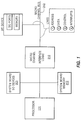
- I/O devices such as displays, keyboards, mice, etc. communicate with the system processor via individual memory and/or I/O addresses. Each individual device is assigned to a set of specific addresses within the system's address space. I/O devices may be physically located either on the system board or on a Micro Channel Adapter Card. Several I/O devices may be grouped on a given Micro Channel Adapter card. Fig. 1 illustrates the System and Micro Channel I/O devices in relation to the rest of the Computer System.
- an Intel 80386 (Intel is a registered trademark of Intel Corporation) or other similar microprocessor 201 is the master processor on the MICRO CHANNEL bus 212, it may be programmed to run multiple virtual processor or multitasking sessions within the same physical processor. Operating the 80386 in this manner is called Virtual 8086 Mode or Protect Mode, respectively. When running in these modes, it is often desirable for each session to have its own individual set of I/O devices. For example, there may be two (or more) sessions running simultaneously, and it would be useful for each session to have its own separate keyboard and display to enable two (or more) individuals to operate the sessions at the same time. If only one set of addresses in the system is allocated for a keyboard, and only one for a display, then the problem becomes one of managing the multiple I/O devices that must share the same set of addresses.
- the new VIRTUAL ENABLED state is a hybrid of the current ACTIVE or ENABLED and INACTIVE or DISABLED states.
- an I/O adapter responds to I/O addressing and presents interrupts to the processor.
- the I/O adapter does not respond to I/O addressing and does not present interrupts.
- the adapter does not respond to I/O addressing (as in the DISABLED state), but will still produce an interrupt (as in the ENABLED state).
- VIR Virtual Identification Register
- VCR Virtual Control Register
- serial adapters can be used, for example, to connect modems, serial printers, etc. to the computer system. Furthermore only two serial adapters will be referenced, though the invention could easily accommodate multiple serial adapters.
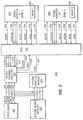
- Processor 201 is preferably an 80386 processor. Additional information on the Intel 80386 can be found in the "INTEL 80386 Programmer's Reference Manual" (Order Number: 230985-001 from INTEL Corp.) which is hereby incorporated by reference. Associated with processor 201 are System Board Memory 202 and System Board I/O Devices 203.
- Microprocessor 201 Communication among microprocessor 201, Memory 202, System Board I/O Devices 203 and MICRO CHANNEL Circuitry 210 is via the 80386 local bus which includes Memory Input/Output (M-I/O) line 204, Address (ADDR) line 206, DATA line 208, and READ/WRITE (R/W) line 209.
- M-I/O Memory Input/Output
- ADDR Address
- R/W READ/WRITE
- M-I/O line 204 indicates whether a particular Address presented on line 206 refers to an address within Memory 202 or I/O Space 203. If the signal on M-I/O 204 is one state then I/O Space 203 is addressed; if the signal is the other state, then System Memory 202 is addressed.
- MICRO CHANNEL bus 212 is the primary data "highway" for all data input/output within the System 200. Between circuitry Block 210 and bus 212 are several lines which transmit various types of information, as follows: Type Function Status lines (3) 214 - Controls Data Transfer DATA line 216 - DATA ADDR line 218 Address for Memory or I/O Space CMD line 220 Indicates beginning and end of data transfer IRQ line 222 Request for processor service
- serial adapters 226 and 226' which share the I/O addresses 3F8-3FF assigned to the serial port designated COM1.
- An expanded view of the I/O space assigned to COM1 can be found in Fig. 3.
- serial adapters 226 and 226' are identical adapters, with each having the same interconnection lines between it and the bus 212. Since they are identical, the lines for serial adapter 226 only will be described, but it is understood that serial adapter 226' has corresponding lines with the prime designation.
- the lines between serial adapter 226 and bus 212 are as follows: Type Function SETUP line 228 Allows card to be setup prior to operational usage STATUS line 230 Controls operation of Bus Cycle DATA line 232 DATA ADDR line 234 Address for Memory or I/O Space IRQ4 line 236 Interrupt service request CMD line 237 Indicates beginning and end of data transfer
- serial adapter #1 (226) and serial adapter #2 (226') must share the I/O address spaces assigned to COM 1, only one of these adapters can be ENABLED at a time, otherwise data would be lost and/or destroyed.
- the Technical Disclosure Bulletin article referenced in the BACKGROUND Section introduces the concept of a logical Virtual Identification Register (VIR) in which each adapter card is assigned a bit for presenting an interrupt(s).
- VIR Virtual Identification Register
- serial adapter 226 could own VIR bit 1 (240) and serial adapter 226' could own VIR bit 2 (240').
- Logically assembling the VIR bits results in the VIR 400 shown in FIG 4 in which adapter 226' is presenting an interrupt in bit #2. Bits 3-8 are not used in this example since there are only 2 serial adapters.
- VCR 500 an additional register called the Virtual Control Register (VCR) 500 is shown.
- VCR 500 is the VCR for all serial adapters sharing the COM 1 port.
- Bit #1 is assigned to Serial Adapter #1 (226)
- Bit #2 is assigned to Serial Adapter #2 (226'). If there were an additional six Serial Adapters sharing COM 1, they would be assigned bits 3-8.
- VCR 500 contains the status information for all of the Serial Adapters sharing the COM1 address space.
- a status of "0" means that the adapter is VIRTUALLY ENABLED. In this state, the adapter does not respond to addressing, but can present interrupts.
- a status of "1” means that the adapter is ACTIVE or ENABLED, i.e. it does respond to addressing and can present interrupts.
- the system will check the VCR to determine the status of that particular adapter to see if the interrupting adapter is the ENABLED adapter (Block 606). If so, the interrupt will be serviced in accordance with normal procedures (Block 608). If not, it will be necessary to change the state of the interrupting adapter from VIRTUAL ENABLED to ENABLED, to permit servicing the interrupt. Since, however, only one adapter can be ENABLED at a time, it will first be necessary to put the ENABLED adapter into the VIRTUAL ENABLED state.
- Block 610 the state of the ENABLED adapter is changed to VIRTUAL ENABLED by clearing (set to “0") its VCR bit.
- Block 612 the state of the VIRTUALLY ENABLED adapter is changed to ENABLED by setting its VCR bit to "1". Now the interrupt can be serviced (Block 608).
Landscapes
- Engineering & Computer Science (AREA)
- Theoretical Computer Science (AREA)
- Physics & Mathematics (AREA)
- General Engineering & Computer Science (AREA)
- General Physics & Mathematics (AREA)
- Bus Control (AREA)
- Computer And Data Communications (AREA)
- Memory System Of A Hierarchy Structure (AREA)
Applications Claiming Priority (2)
| Application Number | Priority Date | Filing Date | Title |
|---|---|---|---|
| US60601290A | 1990-10-30 | 1990-10-30 | |
| US606012 | 1990-10-30 |
Publications (2)
| Publication Number | Publication Date |
|---|---|
| EP0483483A2 true EP0483483A2 (de) | 1992-05-06 |
| EP0483483A3 EP0483483A3 (en) | 1992-08-05 |
Family
ID=24426136
Family Applications (1)
| Application Number | Title | Priority Date | Filing Date |
|---|---|---|---|
| EP19910114684 Ceased EP0483483A3 (en) | 1990-10-30 | 1991-08-31 | Multiple input/output devices having shared address space |
Country Status (7)
| Country | Link |
|---|---|
| US (1) | US5280588A (de) |
| EP (1) | EP0483483A3 (de) |
| JP (1) | JPH0776951B2 (de) |
| KR (1) | KR950012734B1 (de) |
| BR (1) | BR9104314A (de) |
| CA (1) | CA2051199C (de) |
| TW (1) | TW329952U (de) |
Families Citing this family (7)
| Publication number | Priority date | Publication date | Assignee | Title |
|---|---|---|---|---|
| US5454078A (en) * | 1992-08-07 | 1995-09-26 | International Business Machines Corporation | System for sharing name among network adapters by, dynamically linking adapters having same logical name and maintaining linked state of remaining adapters |
| TW276312B (de) * | 1992-10-20 | 1996-05-21 | Cirrlis Logic Inc | |
| US5410709A (en) * | 1992-12-17 | 1995-04-25 | Bull Hn Information System Inc. | Mechanism for rerouting and dispatching interrupts in a hybrid system environment |
| GB9318764D0 (en) * | 1993-09-10 | 1993-10-27 | Wabco Holdings Sab | Improvements relating to friction pads for use in disc brakes |
| US5666556A (en) * | 1993-12-30 | 1997-09-09 | Intel Corporation | Method and apparatus for redirecting register access requests wherein the register set is separate from a central processing unit |
| US5802306A (en) * | 1995-10-31 | 1998-09-01 | International Business Machines Corporation | Supporting multiple client-server sessions from a protocol stack associated with a single physical adapter through use of a plurality of logical adapters |
| JP4461192B1 (ja) | 2009-04-10 | 2010-05-12 | 株式会社東芝 | 電子機器および通信制御方法 |
Family Cites Families (17)
| Publication number | Priority date | Publication date | Assignee | Title |
|---|---|---|---|---|
| GB1397438A (en) * | 1971-10-27 | 1975-06-11 | Ibm | Data processing system |
| US4228504A (en) * | 1978-10-23 | 1980-10-14 | International Business Machines Corporation | Virtual addressing for I/O adapters |
| US4291371A (en) * | 1979-01-02 | 1981-09-22 | Honeywell Information Systems Inc. | I/O Request interrupt mechanism |
| US4320456A (en) * | 1980-01-18 | 1982-03-16 | International Business Machines Corporation | Control apparatus for virtual address translation unit |
| JPS5947625A (ja) * | 1982-09-13 | 1984-03-17 | Fujitsu Ltd | 入出力割り込み方式 |
| JPH0619747B2 (ja) * | 1984-01-18 | 1994-03-16 | 株式会社日立製作所 | I/o命令実行方法、i/o割込処理方法およびそれらを用いた計算機システム |
| US4649479A (en) * | 1985-02-28 | 1987-03-10 | International Business Machines Corp. | Device driver and adapter binding technique |
| US4750113A (en) * | 1985-02-28 | 1988-06-07 | Unisys Corporation | Dual function I/O controller |
| JPS61206043A (ja) * | 1985-03-11 | 1986-09-12 | Hitachi Ltd | 仮想計算機システムにおける割込制御方法 |
| FR2580096B1 (de) * | 1985-04-04 | 1988-08-19 | Nec Corp | |
| US4825358A (en) * | 1985-04-10 | 1989-04-25 | Microsoft Corporation | Method and operating system for executing programs in a multi-mode microprocessor |
| US4779187A (en) * | 1985-04-10 | 1988-10-18 | Microsoft Corporation | Method and operating system for executing programs in a multi-mode microprocessor |
| US4835685A (en) * | 1985-05-06 | 1989-05-30 | Computer X, Inc. | Virtual single machine with message-like hardware interrupts and processor exceptions |
| US4768149A (en) * | 1985-08-29 | 1988-08-30 | International Business Machines Corporation | System for managing a plurality of shared interrupt handlers in a linked-list data structure |
| JPH0814795B2 (ja) * | 1986-01-14 | 1996-02-14 | 株式会社日立製作所 | マルチプロセッサ仮想計算機システム |
| JPH02208740A (ja) * | 1989-02-09 | 1990-08-20 | Fujitsu Ltd | 仮想計算機制御方式 |
| US5185864A (en) * | 1989-06-16 | 1993-02-09 | International Business Machines Corporation | Interrupt handling for a computing system with logical devices and interrupt reset |
-
1991
- 1991-08-01 JP JP3216094A patent/JPH0776951B2/ja not_active Expired - Lifetime
- 1991-08-12 TW TW084201038U patent/TW329952U/zh unknown
- 1991-08-31 EP EP19910114684 patent/EP0483483A3/en not_active Ceased
- 1991-09-11 CA CA002051199A patent/CA2051199C/en not_active Expired - Fee Related
- 1991-10-07 BR BR919104314A patent/BR9104314A/pt unknown
- 1991-10-17 KR KR1019910018292A patent/KR950012734B1/ko not_active Expired - Fee Related
-
1992
- 1992-08-18 US US07/931,650 patent/US5280588A/en not_active Expired - Fee Related
Also Published As
| Publication number | Publication date |
|---|---|
| JPH0776951B2 (ja) | 1995-08-16 |
| US5280588A (en) | 1994-01-18 |
| KR950012734B1 (ko) | 1995-10-20 |
| BR9104314A (pt) | 1992-06-09 |
| CA2051199C (en) | 1996-03-05 |
| EP0483483A3 (en) | 1992-08-05 |
| KR920008602A (ko) | 1992-05-28 |
| JPH04230556A (ja) | 1992-08-19 |
| TW329952U (en) | 1998-04-11 |
| CA2051199A1 (en) | 1992-05-01 |
Similar Documents
| Publication | Publication Date | Title |
|---|---|---|
| US4975838A (en) | Duplex data processing system with programmable bus configuration | |
| US4757441A (en) | Logical arrangement for controlling use of different system displays by main proessor and coprocessor | |
| US4403286A (en) | Balancing data-processing work loads | |
| US4833596A (en) | Logical arrangement for controlling use of different system displays by main processor and co-processor | |
| US5898883A (en) | Memory access mechanism for a parallel processing computer system with distributed shared memory | |
| US5581709A (en) | Multiple computer system using I/O port adaptor to selectively route transaction packets to host or shared I/O device | |
| US5038320A (en) | Computer system with automatic initialization of pluggable option cards | |
| EP0780772A2 (de) | Rechnersystem mit mehreren PC-Kartensteuerungen und Verfahren zur Steuerung von Ein-/Ausgangübertragungen im System | |
| US5109517A (en) | System for selectively controlling slots in an IBM-AT/NEC 9801 dual-compatible computer | |
| US5255372A (en) | Apparatus for efficiently interconnecing channels of a multiprocessor system multiplexed via channel adapters | |
| US5146605A (en) | Direct control facility for multiprocessor network | |
| EP0044949A1 (de) | Dynamisches Terminal-Adressen-Zuweisungsverfahren und Vorrichtung | |
| CA2118995A1 (en) | Arbitration Logic for Multiple Bus Computer System | |
| KR19980041957A (ko) | 프로그램가능 공용 메모리 시스템 및 방법 | |
| EP0284981A2 (de) | Adressierung in einer Computer-Anordnung | |
| US6216196B1 (en) | System and method for multiple device drivers to arbitrate for a single device | |
| EP0483483A2 (de) | Mehrere Ein-/Ausgabeeinrichtungen mit geteiltem Adressraum | |
| US5848294A (en) | PCI computer system with multiple legacy devices | |
| EP0265575B1 (de) | Datenverarbeitungsanordnung mit Vorrichtungen zur automatischen Adresszuordnung zur Adressierung von Schnittstellenmodulen | |
| US5938747A (en) | Hardware command block delivery queue for host adapters and other devices with onboard processors | |
| US6081861A (en) | PCI migration support of ISA adapters | |
| EP0522728B1 (de) | Verfahren zum effizienten Zugriff von Daten in einer Verknüpfungstabelle | |
| EP0316251B1 (de) | Direkte Kontrolleinrichtung für Multiprozessornetzwerk | |
| US6018781A (en) | Work station having simultaneous access to registers contained in two different interfaces | |
| EP0196400B1 (de) | Logische Schaltung zur Steuerung der Benutzung durch den Hauptprozessor und den Coprozessor von verschiedenen Anzeigebetriebsarten |
Legal Events
| Date | Code | Title | Description |
|---|---|---|---|
| PUAI | Public reference made under article 153(3) epc to a published international application that has entered the european phase |
Free format text: ORIGINAL CODE: 0009012 |
|
| AK | Designated contracting states |
Kind code of ref document: A2 Designated state(s): AT CH DE ES FR GB IT LI NL SE |
|
| PUAL | Search report despatched |
Free format text: ORIGINAL CODE: 0009013 |
|
| AK | Designated contracting states |
Kind code of ref document: A3 Designated state(s): AT CH DE ES FR GB IT LI NL SE |
|
| 17P | Request for examination filed |
Effective date: 19920817 |
|
| 17Q | First examination report despatched |
Effective date: 19950714 |
|
| GRAG | Despatch of communication of intention to grant |
Free format text: ORIGINAL CODE: EPIDOS AGRA |
|
| STAA | Information on the status of an ep patent application or granted ep patent |
Free format text: STATUS: THE APPLICATION HAS BEEN REFUSED |
|
| 18R | Application refused |
Effective date: 19970124 |