EP0483494A2 - Circuit pour la mesure de la résistance - Google Patents
Circuit pour la mesure de la résistance Download PDFInfo
- Publication number
- EP0483494A2 EP0483494A2 EP91115303A EP91115303A EP0483494A2 EP 0483494 A2 EP0483494 A2 EP 0483494A2 EP 91115303 A EP91115303 A EP 91115303A EP 91115303 A EP91115303 A EP 91115303A EP 0483494 A2 EP0483494 A2 EP 0483494A2
- Authority
- EP
- European Patent Office
- Prior art keywords
- resistor
- resistance
- measured
- operational amplifier
- resistance measuring
- Prior art date
- Legal status (The legal status is an assumption and is not a legal conclusion. Google has not performed a legal analysis and makes no representation as to the accuracy of the status listed.)
- Withdrawn
Links
Images
Classifications
-
- G—PHYSICS
- G01—MEASURING; TESTING
- G01R—MEASURING ELECTRIC VARIABLES; MEASURING MAGNETIC VARIABLES
- G01R27/00—Arrangements for measuring resistance, reactance, impedance, or electric characteristics derived therefrom
- G01R27/02—Measuring real or complex resistance, reactance, impedance, or other two-pole characteristics derived therefrom, e.g. time constant
Definitions
- the present invention relates to a resistance measuring circuit for generating a voltage output signal which is inversely proportional to a resistance value of a resistance to be measured.
- Such resistance measuring circuits have been known for some time.
- the resistance to be measured lies within the circuit arrangement in such a way that neither of its two connections is connected to ground or to a reference potential.
- high-frequency interference fields such as are present in the measuring environment for most applications of a resistance measuring circuit, lead to a falsification of the resistance measurement or resistance-voltage conversion.
- the resistance to be measured is often located at a location that is comparatively far from the actual converter circuit.
- the resistances of the leads used for the connection of the measuring resistor are included in most resistance measuring circuits as error quantities in the measurement result.
- the lead resistance is compensated for by suitable circuit measures.
- the measuring resistor is not connected to ground or a suitable reference potential, so that again the above-mentioned problems of high-frequency interference from interference fields occur.
- a generic resistance measuring circuit for generating an inversely proportional to a resistance value of a resistance to be measured is Voltage output signals, with a reference voltage source, which is connected with its one pole against a reference potential, and with two operational amplifiers.
- the resistance to be measured lies within the circuit arrangement in such a way that neither of its two connections is connected to ground or to a reference potential.
- high-frequency interference fields such as are present in the measuring environment for most applications, lead to a falsification of the resistance measurement or resistance-voltage conversion.
- a resistance measuring circuit is already known, which is designed as a three-wire measuring circuit.
- the measuring resistor is connected with one pole to a first and second conductor and is connected with its other pole to a third conductor which is at ground potential.
- the second conductor is connected to the non-inverting input of an operational amplifier.
- the first input is connected via a resistor to the inverting input of the operational amplifier, which is connected to its output via a further resistor.
- a current source supplies an impressed current to the connection point of the first conductor with the first resistor.
- a resistance measuring circuit which comprises a differential amplifier, at one input of which the measuring resistor is connected in a negative feedback path, while the other input is connected to an input voltage source, furthermore between the output and the one input of the Differential amplifier is connected a feedback resistor defining the gain factor.
- the present invention is based on the object of developing a resistance measuring circuit of the type mentioned at the outset in such a way that the measuring accuracy is further improved.
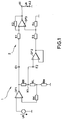
- the resistance measuring circuit which is designated in its entirety by reference number 1, comprises a reference voltage source UR, which is connected with its first pole to a reference potential and a first operational amplifier OP1.
- the non-inverting input of the first operational amplifier is connected to the other pole of the reference voltage source UR.
- the inverting input of the first operational amplifier OP1 is connected via a supply cable, which is indicated here by a resistor RK, to a first connection of a resistor RM to be measured with respect to its resistance value, the second connection of which is connected to ground.
- the output of the first operational amplifier OP1 is connected via a reference resistor RR to a first node K1, which is connected via a second Lead, which is represented by a line resistance RL, is also connected to the first connection of the resistance RM to be measured with respect to its resistance value.
- the resistance RK can also be negligibly small. It is obvious to a person skilled in the art that the level of this resistance has no influence on the function of the circuit insofar as one assumes approximately ideal properties of the first operational amplifier OP1.
- the output of the first operational amplifier OP1 is connected to a first input terminal E1 of a voltage subtraction circuit 2, the second input E2 of which is connected to the first node K1.
- the voltage subtraction circuit generates an output voltage UA on the output side at output connections A1, A2, which corresponds to the differential voltage at its input connections E1, E2, this output voltage UA being related to ground.
- the voltage subtraction circuit comprises a second and a third operational amplifier OP2, OP3 and a resistor circuit explained below.
- the non-inverting input of the second operational amplifier OP2 which works as an impedance converter circuit, is connected to the second input terminal E2, while the inverting input of the second operational amplifier OP2 is connected to its output.
- the inverting input of the third operational amplifier is connected to the first input terminal E1 of the voltage subtraction circuit 2 via a first resistor R1 and is connected to its output A1 via a second resistor R2.
- the non-inverting input of the third operational amplifier OP3 is connected to the output of the second operational amplifier OP2 via a third resistor R3 and to ground via a fourth resistor R4.
- the resistance values of the first, second, third and fourth resistors R1, R2, R3 and R4 are the same.
- the subsequent voltage subtraction circuit 2 has a very high input resistance due to the impedance converter function of the second operational amplifier OP2, so that it is ensured that the current flowing through the reference resistor RR coincides with the current flowing through the measuring resistor RM. It is obvious to a person skilled in the art that the current flowing through the measuring resistor RM corresponds to the quotient of the reference voltage UR to the resistance value of the measuring resistor RM.
- the output voltage UA corresponds to the difference in the potentials at their input terminals E1, E2. It follows from this that the output voltage of the negative reference voltage multiplied by the quotient of the resistance value of the reference resistor RR is equal to that of the resistor RM to be measured. It can be seen that in the circuit according to the invention the resistance value of the resistors RK and RL is not included in the output voltage, so that the lead resistance is not important.
- the resistance to be measured is connected to ground, so that high-frequency interference can be shielded well.
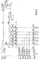
- FIG. 2 A second embodiment of the resistance-voltage converter according to the invention is explained in more detail below with reference to FIG. 2.
- the embodiment according to FIG. 1 which is designated in its entirety by the reference symbol 1 ', comprises a plurality N of resistors RM1, RM2, RM3,..., RMN to be measured, which alternatively both by means of a first and second switch arrangement S1, S2 can be switched to the first node K1 and also to the inverting input of the first operational amplifier OP1.
- the first switch arrangement S1 comprises a plurality N of first switches S11 to S1N corresponding to the plurality N of resistors RM1 to RMN to be measured.
- the first switches S11 to S1N are connected to one contact with the inverting input of the first operational amplifier OP1 and to the other contact with the first connection in each case one of the resistors RM1 to RMN to be measured.
- the switch resistances of the individual switches which also include the lead resistances, are represented by the equivalent resistors RK1, RK2, ..., RKN.
- the second switch arrangement likewise comprises a plurality N of second switches S21 to S2N corresponding to the plurality N of resistors RM1 to RMN to be measured.
- the second switches S21 to S2N are connected to one contact with the first connection of each of the resistors RM1 to RMN to be measured and to the other contact with the reference resistor RR.
- the equivalent resistors RL1, RL2, ..., RLN assigned to the switches denote the volume resistance of a closed switch and the resistance of the connecting lead.
- an associated resistance RMI to be measured can be measured with respect to its resistance value. Neither lead resistances nor switch resistances are included in the measurement result.
Landscapes
- Physics & Mathematics (AREA)
- General Physics & Mathematics (AREA)
- Measurement Of Resistance Or Impedance (AREA)
Applications Claiming Priority (2)
| Application Number | Priority Date | Filing Date | Title |
|---|---|---|---|
| DE4034699U | 1990-10-31 | ||
| DE19904034699 DE4034699C1 (en) | 1990-10-31 | 1990-10-31 | Resistance measuring circuit using voltage transducer - has operational amplifier with non-inverted input connected to reference voltage source |
Publications (2)
| Publication Number | Publication Date |
|---|---|
| EP0483494A2 true EP0483494A2 (fr) | 1992-05-06 |
| EP0483494A3 EP0483494A3 (en) | 1992-05-27 |
Family
ID=6417415
Family Applications (1)
| Application Number | Title | Priority Date | Filing Date |
|---|---|---|---|
| EP19910115303 Withdrawn EP0483494A3 (en) | 1990-10-31 | 1991-09-10 | Circuit for measuring the resistance |
Country Status (2)
| Country | Link |
|---|---|
| EP (1) | EP0483494A3 (fr) |
| DE (1) | DE4034699C1 (fr) |
Cited By (2)
| Publication number | Priority date | Publication date | Assignee | Title |
|---|---|---|---|---|
| DE4304448A1 (de) * | 1993-02-13 | 1994-09-15 | Ita Ingb Testaufgaben Gmbh | Guard-Testvorrichtung |
| CN108508270A (zh) * | 2018-04-08 | 2018-09-07 | 佛山科学技术学院 | 一种电阻测量电路 |
Family Cites Families (5)
| Publication number | Priority date | Publication date | Assignee | Title |
|---|---|---|---|---|
| DE1281570B (de) * | 1966-06-08 | 1969-04-30 | Boelkow Gmbh | Schaltung zum Abbilden der AEnderung des Widerstandes eines Messobjektes als proportionale elektrische Spannung oder als solcher Strom |
| DE2122561A1 (de) * | 1971-05-07 | 1972-11-09 | Siemens AG, 1000 Berlin u. 8000 München | Meßverstärker |
| SE378460B (fr) * | 1974-01-30 | 1975-09-01 | Tillquist Ab Hugo | |
| EP0039751A1 (fr) * | 1980-05-08 | 1981-11-18 | Imperial Chemical Industries Plc | Mesure de la résistance électrique |
| DE3918695C1 (en) * | 1989-06-08 | 1990-09-13 | Digi-Table Thielen Gmbh & Co Kg, 4300 Essen, De | Resistance measuring circuit with differential amplifier - has voltage measurement device with input differential amplifier, and constant current source |
-
1990
- 1990-10-31 DE DE19904034699 patent/DE4034699C1/de not_active Expired - Lifetime
-
1991
- 1991-09-10 EP EP19910115303 patent/EP0483494A3/de not_active Withdrawn
Cited By (3)
| Publication number | Priority date | Publication date | Assignee | Title |
|---|---|---|---|---|
| DE4304448A1 (de) * | 1993-02-13 | 1994-09-15 | Ita Ingb Testaufgaben Gmbh | Guard-Testvorrichtung |
| CN108508270A (zh) * | 2018-04-08 | 2018-09-07 | 佛山科学技术学院 | 一种电阻测量电路 |
| CN108508270B (zh) * | 2018-04-08 | 2023-09-08 | 佛山科学技术学院 | 一种电阻测量电路 |
Also Published As
| Publication number | Publication date |
|---|---|
| DE4034699C1 (en) | 1991-12-19 |
| EP0483494A3 (en) | 1992-05-27 |
Similar Documents
| Publication | Publication Date | Title |
|---|---|---|
| DE69915816T2 (de) | Strommessvorrichtung | |
| DE2619448C2 (de) | Ringförmiger Beschleunigungsmesser | |
| DE3611261C2 (fr) | ||
| DE2917237C2 (fr) | ||
| DE3437378C2 (de) | Audio-Empfänger mit symmetrischem Basisband | |
| DE3831659A1 (de) | Einschaltung zum eichen eines ohmmeters | |
| DE3686111T2 (de) | Teilnehmerleitungsschnittstellenschaltung mit mitteln zum kombinieren von gleichstrom- und wechselstromgegenkopplungssignalen. | |
| DE69530715T2 (de) | Messvorrichtung für eine elektrische Grösse | |
| DE1648873A1 (de) | Feuchtigkeitsmessvorrichtung | |
| DE4101492C2 (fr) | ||
| DE2420377A1 (de) | Elektrischer messumformer nach dem zwei-draht-verfahren | |
| DE1438969A1 (de) | Gleichstromregelungsgeraet | |
| DE2428082C3 (de) | Schaltangsanordnung zur Eichung einer Meßanordnung zur Volumen-Messung von Partikeln | |
| DE3043053C1 (de) | Schaltungsanordnung zur Auswertung von Signalen | |
| EP0489259A2 (fr) | Convertisseur capacité-fréquence | |
| EP0483494A2 (fr) | Circuit pour la mesure de la résistance | |
| DE2353812C3 (de) | Temperaturmeßschaltung | |
| DE2714142A1 (de) | Einrichtung zur messung eines magnetflusses | |
| DE2214430C3 (de) | Gerät zum Umwandeln einer von einer nicht elektrischen Größe abgeleiteten Meßspannung in eine zweite Spannung | |
| DE2202501B2 (de) | Aus negativen Widerstanden bestehen der Vierpol zur reflexionsarmen Dampfungs verminderung einer Zweidrahtleitung | |
| DE2810951C2 (de) | Kompensationsschaltung für elektronische Meßgeräte | |
| DE4135990C1 (en) | Capacitance-frequency converter with offset compensation - has third changeover switch connected to compensating capacitor for switching to different potentials | |
| DE3027800C2 (de) | Schaltungsanordnung zur Vermeidung von Störspannungen bei Messungen mit Gleichstrom-Murray-Brückenschaltungen an Kabeln | |
| DE4211980C1 (en) | Current-voltage converter for measuring appts. - has parallel electronic circuit paths acting as voltage divider and regulated voltage divider with centre tap-offs providing positive and negative output voltage nodes | |
| EP0037940A1 (fr) | Circuit pour branchement à deux fils d'un abonné téléphonique à une ligne pour des signaux sortants et une ligne pour des signaux entrants |
Legal Events
| Date | Code | Title | Description |
|---|---|---|---|
| PUAI | Public reference made under article 153(3) epc to a published international application that has entered the european phase |
Free format text: ORIGINAL CODE: 0009012 |
|
| PUAL | Search report despatched |
Free format text: ORIGINAL CODE: 0009013 |
|
| AK | Designated contracting states |
Kind code of ref document: A2 Designated state(s): AT DE FR GB NL |
|
| AK | Designated contracting states |
Kind code of ref document: A3 Designated state(s): AT DE FR GB NL |
|
| 17P | Request for examination filed |
Effective date: 19920521 |
|
| 17Q | First examination report despatched |
Effective date: 19940103 |
|
| STAA | Information on the status of an ep patent application or granted ep patent |
Free format text: STATUS: THE APPLICATION IS DEEMED TO BE WITHDRAWN |
|
| 18D | Application deemed to be withdrawn |
Effective date: 19950221 |