EP0483530A2 - Méthode et dispositif pour l'harmonisation du décalage et de la réponse dans un détecteur électro-optique linéaire ou mosaique - Google Patents
Méthode et dispositif pour l'harmonisation du décalage et de la réponse dans un détecteur électro-optique linéaire ou mosaique Download PDFInfo
- Publication number
- EP0483530A2 EP0483530A2 EP91116657A EP91116657A EP0483530A2 EP 0483530 A2 EP0483530 A2 EP 0483530A2 EP 91116657 A EP91116657 A EP 91116657A EP 91116657 A EP91116657 A EP 91116657A EP 0483530 A2 EP0483530 A2 EP 0483530A2
- Authority
- EP
- European Patent Office
- Prior art keywords
- detector
- image
- detectors
- offset
- radiation
- Prior art date
- Legal status (The legal status is an assumption and is not a legal conclusion. Google has not performed a legal analysis and makes no representation as to the accuracy of the status listed.)
- Granted
Links
Images


Classifications
-
- H—ELECTRICITY
- H04—ELECTRIC COMMUNICATION TECHNIQUE
- H04N—PICTORIAL COMMUNICATION, e.g. TELEVISION
- H04N1/00—Scanning, transmission or reproduction of documents or the like, e.g. facsimile transmission; Details thereof
- H04N1/04—Scanning arrangements, i.e. arrangements for the displacement of active reading or reproducing elements relative to the original or reproducing medium, or vice versa
- H04N1/19—Scanning arrangements, i.e. arrangements for the displacement of active reading or reproducing elements relative to the original or reproducing medium, or vice versa using multi-element arrays
- H04N1/191—Scanning arrangements, i.e. arrangements for the displacement of active reading or reproducing elements relative to the original or reproducing medium, or vice versa using multi-element arrays the array comprising a one-dimensional [1D] array
- H04N1/1911—Simultaneously or substantially simultaneously scanning picture elements on more than one main scanning line, e.g. scanning in swaths
- H04N1/1913—Scanning adjacent picture elements in different scans of the array, e.g. in complementary checkerboard patterns
- H04N1/1915—Scanning adjacent picture elements in different scans of the array, e.g. in complementary checkerboard patterns with subscan displacement of the array between successive scans
-
- H—ELECTRICITY
- H04—ELECTRIC COMMUNICATION TECHNIQUE
- H04N—PICTORIAL COMMUNICATION, e.g. TELEVISION
- H04N25/00—Circuitry of solid-state image sensors [SSIS]; Control thereof
- H04N25/20—Circuitry of solid-state image sensors [SSIS]; Control thereof for transforming only infrared radiation into image signals
- H04N25/21—Circuitry of solid-state image sensors [SSIS]; Control thereof for transforming only infrared radiation into image signals for transforming thermal infrared radiation into image signals
-
- H—ELECTRICITY
- H04—ELECTRIC COMMUNICATION TECHNIQUE
- H04N—PICTORIAL COMMUNICATION, e.g. TELEVISION
- H04N1/00—Scanning, transmission or reproduction of documents or the like, e.g. facsimile transmission; Details thereof
- H04N1/04—Scanning arrangements, i.e. arrangements for the displacement of active reading or reproducing elements relative to the original or reproducing medium, or vice versa
- H04N1/19—Scanning arrangements, i.e. arrangements for the displacement of active reading or reproducing elements relative to the original or reproducing medium, or vice versa using multi-element arrays
- H04N1/195—Scanning arrangements, i.e. arrangements for the displacement of active reading or reproducing elements relative to the original or reproducing medium, or vice versa using multi-element arrays the array comprising a two-dimensional [2D] array
- H04N1/19505—Scanning picture elements spaced apart from one another in at least one direction
- H04N1/1951—Scanning picture elements spaced apart from one another in at least one direction in one direction
-
- H—ELECTRICITY
- H04—ELECTRIC COMMUNICATION TECHNIQUE
- H04N—PICTORIAL COMMUNICATION, e.g. TELEVISION
- H04N23/00—Cameras or camera modules comprising electronic image sensors; Control thereof
- H04N23/58—Means for changing the camera field of view without moving the camera body, e.g. nutating or panning of optics or image sensors
-
- H—ELECTRICITY
- H04—ELECTRIC COMMUNICATION TECHNIQUE
- H04N—PICTORIAL COMMUNICATION, e.g. TELEVISION
- H04N25/00—Circuitry of solid-state image sensors [SSIS]; Control thereof
- H04N25/60—Noise processing, e.g. detecting, correcting, reducing or removing noise
- H04N25/67—Noise processing, e.g. detecting, correcting, reducing or removing noise applied to fixed-pattern noise, e.g. non-uniformity of response
- H04N25/671—Noise processing, e.g. detecting, correcting, reducing or removing noise applied to fixed-pattern noise, e.g. non-uniformity of response for non-uniformity detection or correction
- H04N25/672—Noise processing, e.g. detecting, correcting, reducing or removing noise applied to fixed-pattern noise, e.g. non-uniformity of response for non-uniformity detection or correction between adjacent sensors or output registers for reading a single image
-
- H—ELECTRICITY
- H04—ELECTRIC COMMUNICATION TECHNIQUE
- H04N—PICTORIAL COMMUNICATION, e.g. TELEVISION
- H04N25/00—Circuitry of solid-state image sensors [SSIS]; Control thereof
- H04N25/48—Increasing resolution by shifting the sensor relative to the scene
Definitions
- the invention is primarily but not exclusively useful for radiation receivers which are used in the infrared spectral range (approx. 2 ⁇ m to 14 ⁇ m) in thermal imaging devices. For physical and technological reasons, certain detector defects in this spectral range are much more critical than in the visible. These are offset or differences in offset and differences in responsiveness.
- the current or voltage that is not caused by the signal radiation is sometimes referred to as offset, sometimes also referred to as dark or leakage current or voltage. Responsiveness is the change in current or voltage as a function of a change in radiation to a detector, the change in radiation generally being assumed to be proportional to the change in temperature.
- the harmonization can be carried out using a microscan.
- a microscan is known from the company magazine "Kontron Image Analysis, Prog. Res. 3000, Production Formation” from June 1989, pp. 2-15.
- two detectors can each assume identical positions in relation to the image or object space. To restore the resolution of the original black and white image, different color information is superimposed. There is nothing in this document to show that such a “staggering" can be useful for harmonizing offset and responsiveness.
- a detector system in which each of the elements takes on four positions in succession due to the scanning movement of a mirror, which roughly correspond to the corner points of a rectangle - the simplest possible case - is e.g. known from EP-A-0 133 890.
- a disadvantage of this embodiment is the very specific definition of only four scanning positions.
- the nutating movement of the mirror also requires a gimbal that is comparatively complex.
- Integrated semiconductor detectors are then known for television cameras in the visible range, which consist, for example, of 580 x 700 detector elements.
- the signals are read out using CCDs (charged coupled devices). It is characteristic of this type of detector elements that each of them corresponds to a pixel. The resolution of an image therefore depends on the number of detectors.
- conventional thermal imaging devices use a few detector elements, a maximum of about 100, which are guided over the image field by means of mechanical-optical methods, so that such a mosaic detector delivers signals from many pixels.
- increasing the number of detectors to values that are used in the visible in CCDs encounters cost and technological problems in the infrared.
- HgCdTe mercury cadmium telluride
- mosaics of at most approximately 128 x 128 to a maximum of 256 x 256 detector elements are acceptable in this regard.
- Another problem is represented by the spaces between the detectors. Often they are comparatively large for technological reasons, so that a lot of radiation also falls into this insensitive area. This not only reduces the sensitivity of the arrangement, but additional information is lost, which contributes to falsification of the image. This phenomenon is known as "aliasing".
- the object of the invention is seen in the creation of an inexpensive, deterministic method for harmonization for offset voltages and different responsivities; this task can also be linked to the known task of eliminating or reducing the aliasing phenomenon.
- This object is achieved according to the invention by the characterizing features of claim 1. With a comparatively simple networking, a scene (temperature) related deterministic offset correction and responsiveness harmonization can be carried out.
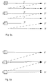
- FIG. 1a shows the principle of compensation. It shows the compensated output voltage of two detectors 1 and 2, which are arranged according to FIG. 1b. Detector 1 is moved from its rest position 1 'to position 2' (the rest position of detector 2) and optionally to position 5 '. Detector 2 is then in turn moved from position 2 'to 5' (and optionally to n ').
- the scene radiation (temperature) in FIG. 1 may increase from left to right, so that the output voltages of the detectors also increase. Because of the detector inhomogeneities, these output voltages will be different. But now the detectors in position 2 'receive the same amount of radiation. This allows electrical compensation of the output voltage ( offset compensation).
- Fig. 2a a section of four detector elements 1 to 4 is assumed from a mosaic detector in which a conventional two-by-two microscan is carried out.
- the detector element 1 assumes the positions 1 ', a, c and d one after the other.
- the aliasing problem is addressed in that the positions a, c and d fall into spaces between the individual detector elements.
- FIG. 2b networking is carried out which can serve to harmonize the offset and responsiveness according to FIG. 1: If detector 1 takes positions 1 ', 2' 4 'and 3' one after the other, detector 2 takes, among other things Positions 2 'and 4'.
- FIG. 3 which shows a larger section of the mosaic according to FIG. 2, demonstrates the principle according to FIGS. 2a and 2b, that is to say the conventional microscan and the networking.
- the detector 1 takes, for example, the positions 1 ', a, 2', b, c, d, 3 ', e, 4' one after the other, the positions denoted by the letters a to e denoting a conventional microscan for filling the gaps , whereas positions 1 ', 2' 3 'and 4' are used for networking and thus for the harmonization of offset and reponsiveness (gain).
- the conventional scanning method of FIG. 2a can also be used to extrapolate to harmonize offset and responsiveness, see FIG. 4.
- the geometric arrangement corresponds to FIG. 3: If detector 1 is moved from position 1 'to a, then Because of the small change in location, the voltage of detector 1 at position 2 'can be predicted with good approximation by linear extrapolation. However, offset harmonization with detector 2 is possible as a result. The extrapolation error will be even smaller if the harmonization is done by averaging, since - provided that the scene does not remain constant - the deviations from linearity will be zero on average.
- the voltage of the detector 1 is extrapolated from a to 2 '.
- the voltage of the detector 2 can be extrapolated from position 2 'to a, so that the output voltage for two identical positions (a and 2') is known, albeit extrapolated, for two detectors. This again results in the case that the identical change in radiation can be used to harmonize the responsiveness of detectors 1 and 2.
- two detectors each receive the same amount of radiation. This can also be done by defocusing. This results in an averaging over a certain area of the scene which is dependent on the degree of defocusing and which can be adapted to the scene content. If one now selects a second position of the defocusing, one will generate a radiation field which corresponds to an average value, but which will differ from the first-mentioned average value. This results in a change in the radiation which is identical in the case of neighboring detectors and can thus harmonize the responsiveness (gain) .
- the compensation voltages are expediently determined by averaging from many measurements.
- the averaging ensures that the harmonization voltages or harmonization coefficients are not impaired by the noise of the detectors in the limit case. Since the harmonization changes only slightly from one image to the next, the noise of the system will only increase insignificantly. Finally, this ensures that the compensation for sudden changes, e.g. the lighting up of a point object, does not compensate for the useful signal.
- FIG. 5a shows in a line detector a conventional line interlacing method (interlace) in which detector 1, after passing through line 1 ′′, also scans line a ′ between the rest position of detectors 1 and 2.
- Fig. 5b shows the application of the method according to the invention: Here gropes detector 1 lines 1 '' and line 2 '', detector 2 lines 2 '' and 3 ''. 6 shows an example of the output signals of detectors 1 and 2 for line 2 ′′.
- the mean values of the detector voltages U 1 and U 2 are different, but can be compensated for in accordance with the method according to the invention, since the same scene radiation is present. Because of the different responsivities, the deviations from the mean will also be different. These inequalities can also be compensated for by determining the fluctuations around said mean value, for example measuring the effective value of the AC voltage component (RMS value).
- RMS value effective value
- a mirror is usually used for scanning.
- these systems work unidirectionally, i.e. the mirror is used to scan the scene for image acquisition, for example, from left to right, the return of the mirror to the starting position (from right to left) is not used for image acquisition, among other things because with detector arrangements with TDI (time-delayed integration ) this TDI only leads to a meaningful image structure in one direction. If the electrical integration is nevertheless carried out in the case of a mirror return, the integrated signals will not come from identical pixels, rather the output signal will be the average of a number of points which are close together.
- U i , U j , U k are voltages of detectors 100 which are linked in an intermediate layer 101 and deliver harmonized responsivities R i , R j , R k 102 at the output .
- FIG. 8 shows a section of a mosaic detector in which the image shifting means 20 (FIG. 9), e.g. a scanning mirror or a transparent plate, by means of electromagnetic force, which performs nutating movement in accordance with the rectangular scanning loop, which is state of the art.
- the image shifting means 20 e.g. a scanning mirror or a transparent plate
- electromagnetic force which performs nutating movement in accordance with the rectangular scanning loop
- the image shifting means 20 is held in the center on its right end 15 in the direction of view by means of a ball bearing 16.
- joints, torsion bars, torsion springs and the like are also used for the holder. conceivable without thereby leaving the scope of the invention. In each of these cases, however, the storage or suspension must take place in such a way that the image shifting means can both be rotated about the axis of symmetry running through the attachment point and tilted in the plane perpendicular to the image shifting means.
- a specially designed magnetic drive and positioning magnet system 19-13 or 19'-13 ' is then provided in the corner areas of the opposite end face 17, which is the subject of the following description:
- the mirror or the transparent plate each have these areas a permanent magnet 19 or 19 'attached, the free end, for example to represent the South Pole.
- Opposite these south poles is e.g. each have an essentially U-shaped structure, the leg 10 or 10 'of which is also a permanent magnet, has a pole shoe made of soft iron and acts accordingly as the north pole.
- the leg 11 or 11 ' consists of an electromagnet with the two coils 12 and 13 or 12' and 13 '. If leg 11 or 11 'is magnetized via excitation coil 12 and a corresponding current flow in such a way that its forces with the same polarity are as strong as those of leg 10 or 10', the image shifting means 20 and its two magnets 19 and 19 'take a middle position between the two legs 10 and 11. If, on the other hand, the current in the coil 12 or 12 'becomes stronger or weaker, the image shifting means and magnets assume a correspondingly eccentric position, that is to say the same then find their rest position somewhat more in the direction of the legs 10 or 11 or 10' or 11 '.
- the image offset means 20 moves up and down with its magnet-side end in the direction of the double arrow 18, which is also referred to as a tilting movement. If, on the other hand, the magnets are excited in opposite directions, the image shifting means rotates around the axis of symmetry running through its attachment point 16.
- the two drive circuits for rotary and tilting movements can be separated by starting up the second coil 13 or 13 ', coil 12 from leg 11 with coil 12' from leg 11 'being excited in the same direction and coil 13 with coil 13' being excited in opposite directions.
- FIG. 10 Another embodiment of the invention is shown in FIG. 10.
- the image displacement means 20 also with all four corners or via corresponding permanent magnets 19 to 19 '' 'in magnetic drive and positioning magnet systems 10, 11, 12, 13, to 10 '' ', 11' '', 12 '' ', 13' '' can be stored.
- the control described above - now all eight coils 12, 13 to 12 '' ', 13' '' - can cause a nutation or wobble movement of the mirror.
- the storage of a corner point is drawn out on its own and on an enlarged scale, and it can also be seen that the maximum "stroke" of the nutation or wobble movement is determined by the distance of the mirror from the two legs.
Landscapes
- Engineering & Computer Science (AREA)
- Multimedia (AREA)
- Signal Processing (AREA)
- Transforming Light Signals Into Electric Signals (AREA)
Applications Claiming Priority (4)
| Application Number | Priority Date | Filing Date | Title |
|---|---|---|---|
| DE19904034488 DE4034488C1 (en) | 1990-10-30 | 1990-10-30 | Scanning system for electro=optical mosaic detector - has image offsetting plate facing magnetic drive and positioning system for rotating and tilting |
| DE4034488 | 1990-10-30 | ||
| DE4039577A DE4039577A1 (de) | 1990-12-12 | 1990-12-12 | Abtastverfahren fuer einen elektrooptischen zeilen- oder mosaikdetektor |
| DE4039577 | 1990-12-12 |
Publications (3)
| Publication Number | Publication Date |
|---|---|
| EP0483530A2 true EP0483530A2 (fr) | 1992-05-06 |
| EP0483530A3 EP0483530A3 (en) | 1992-09-23 |
| EP0483530B1 EP0483530B1 (fr) | 1996-06-12 |
Family
ID=25898111
Family Applications (1)
| Application Number | Title | Priority Date | Filing Date |
|---|---|---|---|
| EP91116657A Expired - Lifetime EP0483530B1 (fr) | 1990-10-30 | 1991-09-30 | Méthode et dispositif pour l'harmonisation du décalage et de la réponse dans un détecteur électro-optique linéaire ou mosaique |
Country Status (2)
| Country | Link |
|---|---|
| EP (1) | EP0483530B1 (fr) |
| DE (1) | DE59107923D1 (fr) |
Cited By (17)
| Publication number | Priority date | Publication date | Assignee | Title |
|---|---|---|---|---|
| WO1993025043A1 (fr) * | 1992-05-29 | 1993-12-09 | The Secretary Of State For Defence In Her Britannic Majesty's Government | Systeme de formation d'image a dissimulation d'element mort |
| EP0600742A1 (fr) * | 1992-12-04 | 1994-06-08 | Hughes Aircraft Company | Système sensoriel avec suppression de non-uniformité et préservation d'image |
| DE4436306C1 (de) * | 1994-10-11 | 1995-11-30 | Siemens Ag | Röntgendiagnostikeinrichtung mit einer Bildverstärker-Fernsehkette |
| FR2725101A1 (fr) * | 1994-09-23 | 1996-03-29 | Thomson Csf | Camera thermique a matrice de detection |
| NL1003131C2 (nl) * | 1996-05-15 | 1997-11-18 | Tno | Inrichting en werkwijze voor het voor niet-uniformiteit corrigeren van met behulp van een beeldopnemer verkregen beeldsignalen. |
| FR2756129A1 (fr) * | 1996-11-15 | 1998-05-22 | Sagem | Camera video a deviateur d'augmentation de resolution |
| WO1998026582A1 (fr) * | 1996-12-09 | 1998-06-18 | Raytheon Company | Correction de decalage de balayage par vibrations |
| EP0871327A1 (fr) | 1997-04-07 | 1998-10-14 | Canon Denshi Kabushiki Kaisha | Dispositif de prise de vue ayant une plaque de décalage d'image |
| EP0899944A2 (fr) | 1997-08-28 | 1999-03-03 | Canon Denshi Kabushiki Kaisha | Appareil de prise de vues utilisant le décalage des pixels |
| EP0853425A3 (fr) * | 1997-01-14 | 1999-05-26 | Canon Denshi Kabushiki Kaisha | Dispositif de prise de vue |
| FR2792149A1 (fr) * | 1999-04-12 | 2000-10-13 | Commissariat Energie Atomique | Procede de formation d'une image |
| NL1013296C2 (nl) * | 1999-10-14 | 2001-04-18 | Hollandse Signaalapparaten Bv | Detectieinrichting voorzien van offsetcompensatie. |
| EP1301027A1 (fr) * | 2001-10-05 | 2003-04-09 | Abscondenda AB | Méthode et dispositif pour améliorer la résolution d'images ou pour comparer des images gràce à un traitement parallèle à grande vitesse |
| WO2007025832A1 (fr) * | 2005-08-03 | 2007-03-08 | Thales Holdings Uk Plc | Appareil et procede d'imagerie |
| US7307653B2 (en) * | 2001-10-19 | 2007-12-11 | Nokia Corporation | Image stabilizer for a microcamera module of a handheld device, and method for stabilizing a microcamera module of a handheld device |
| US9251595B2 (en) | 2013-03-15 | 2016-02-02 | Drs Network & Imaging Systems, Llc | Method of shutterless non-uniformity correction for infrared imagers |
| US10070075B2 (en) | 2013-03-14 | 2018-09-04 | Drs Network & Imaging Systems, Llc | Method and system for providing scene data in a video stream |
Family Cites Families (8)
| Publication number | Priority date | Publication date | Assignee | Title |
|---|---|---|---|---|
| US4345148A (en) * | 1980-10-06 | 1982-08-17 | Hughes Aircraft Company | Automatic responsivity control for a CCD imager |
| US4509077A (en) * | 1982-12-17 | 1985-04-02 | Ncr Canada Ltd-Ncr Canada Ltee | Automatic, self-diagnosing, electro-optical imaging system |
| JPS59186481A (ja) * | 1983-04-08 | 1984-10-23 | Citizen Watch Co Ltd | 撮像装置 |
| GB2149605B (en) * | 1983-11-04 | 1987-06-10 | Marconi Avionics | Image processing |
| FR2573263B1 (fr) * | 1984-11-12 | 1988-05-06 | Telecommunications Sa | Perfectionnement aux systemes d'imagerie a balayage |
| WO1986006214A1 (fr) * | 1985-04-08 | 1986-10-23 | Irvine Sensors Corporation | Dispositif d'imagerie thermique ayant un senseur dans un module electronique |
| US4876453A (en) * | 1986-02-19 | 1989-10-24 | Hughes Aircraft Company | Method and apparatus for calibrating an imaging sensor |
| JPH02206976A (ja) * | 1989-02-06 | 1990-08-16 | Fujitsu Ltd | 赤外線撮像装置の感度補正方法 |
-
1991
- 1991-09-30 DE DE59107923T patent/DE59107923D1/de not_active Expired - Lifetime
- 1991-09-30 EP EP91116657A patent/EP0483530B1/fr not_active Expired - Lifetime
Cited By (30)
| Publication number | Priority date | Publication date | Assignee | Title |
|---|---|---|---|---|
| WO1993025043A1 (fr) * | 1992-05-29 | 1993-12-09 | The Secretary Of State For Defence In Her Britannic Majesty's Government | Systeme de formation d'image a dissimulation d'element mort |
| EP0600742A1 (fr) * | 1992-12-04 | 1994-06-08 | Hughes Aircraft Company | Système sensoriel avec suppression de non-uniformité et préservation d'image |
| FR2725101A1 (fr) * | 1994-09-23 | 1996-03-29 | Thomson Csf | Camera thermique a matrice de detection |
| DE4436306C1 (de) * | 1994-10-11 | 1995-11-30 | Siemens Ag | Röntgendiagnostikeinrichtung mit einer Bildverstärker-Fernsehkette |
| NL1003131C2 (nl) * | 1996-05-15 | 1997-11-18 | Tno | Inrichting en werkwijze voor het voor niet-uniformiteit corrigeren van met behulp van een beeldopnemer verkregen beeldsignalen. |
| US6249312B1 (en) | 1996-11-15 | 2001-06-19 | Sagem Sa | Video camera having deviating means for improving resolution |
| FR2756129A1 (fr) * | 1996-11-15 | 1998-05-22 | Sagem | Camera video a deviateur d'augmentation de resolution |
| WO1998026582A1 (fr) * | 1996-12-09 | 1998-06-18 | Raytheon Company | Correction de decalage de balayage par vibrations |
| US6011584A (en) * | 1996-12-09 | 2000-01-04 | Raytheon Company | Method and apparatus for correcting offsets of two detectors using respective functions of a difference |
| EP0853425A3 (fr) * | 1997-01-14 | 1999-05-26 | Canon Denshi Kabushiki Kaisha | Dispositif de prise de vue |
| US6771310B1 (en) | 1997-01-14 | 2004-08-03 | Canon Denshi Kabushiki Kaisha | Image pickup apparatus with optical beam shifting with independently controlled optical elements |
| US6473121B1 (en) | 1997-04-07 | 2002-10-29 | Canon Denshi Kabushiki Kaisha | Image pickup apparatus with optical element movable among a plurality of inclination positions |
| EP0871327A1 (fr) | 1997-04-07 | 1998-10-14 | Canon Denshi Kabushiki Kaisha | Dispositif de prise de vue ayant une plaque de décalage d'image |
| EP0899944A2 (fr) | 1997-08-28 | 1999-03-03 | Canon Denshi Kabushiki Kaisha | Appareil de prise de vues utilisant le décalage des pixels |
| EP0899944A3 (fr) * | 1997-08-28 | 1999-05-26 | Canon Denshi Kabushiki Kaisha | Appareil de prise de vues utilisant le décalage des pixels |
| US6753906B2 (en) | 1997-08-28 | 2004-06-22 | Canon Kabushiki Kaisha | Image sensing apparatus utilizing pixel-shifting |
| FR2792149A1 (fr) * | 1999-04-12 | 2000-10-13 | Commissariat Energie Atomique | Procede de formation d'une image |
| WO2001028233A1 (fr) * | 1999-10-14 | 2001-04-19 | Thales Nederland B.V. | Dispositif de detection a compensation de decalage |
| US6723992B1 (en) | 1999-10-14 | 2004-04-20 | Thales Nederland B.V. | Detection arrangement provided with offset compensation |
| NL1013296C2 (nl) * | 1999-10-14 | 2001-04-18 | Hollandse Signaalapparaten Bv | Detectieinrichting voorzien van offsetcompensatie. |
| EP1301027A1 (fr) * | 2001-10-05 | 2003-04-09 | Abscondenda AB | Méthode et dispositif pour améliorer la résolution d'images ou pour comparer des images gràce à un traitement parallèle à grande vitesse |
| US7307653B2 (en) * | 2001-10-19 | 2007-12-11 | Nokia Corporation | Image stabilizer for a microcamera module of a handheld device, and method for stabilizing a microcamera module of a handheld device |
| WO2007025832A1 (fr) * | 2005-08-03 | 2007-03-08 | Thales Holdings Uk Plc | Appareil et procede d'imagerie |
| US10070075B2 (en) | 2013-03-14 | 2018-09-04 | Drs Network & Imaging Systems, Llc | Method and system for providing scene data in a video stream |
| US10104314B2 (en) | 2013-03-14 | 2018-10-16 | Drs Network & Imaging Systems, Llc | Methods and system for producing a temperature map of a scene |
| US10694120B2 (en) | 2013-03-14 | 2020-06-23 | Drs Network & Imaging Systems, Llc | Methods for producing a temperature map of a scene |
| US10701289B2 (en) | 2013-03-14 | 2020-06-30 | Drs Network & Imaging Systems, Llc | Method and system for providing scene data in a video stream |
| US9251595B2 (en) | 2013-03-15 | 2016-02-02 | Drs Network & Imaging Systems, Llc | Method of shutterless non-uniformity correction for infrared imagers |
| US9508124B2 (en) | 2013-03-15 | 2016-11-29 | Drs Network & Imaging Systems, Llc | Method of shutterless non-uniformity correction for infrared imagers |
| US10462388B2 (en) | 2013-03-15 | 2019-10-29 | Drs Network & Imaging Systems, Llc | Method of shutterless non-uniformity correction for infrared imagers |
Also Published As
| Publication number | Publication date |
|---|---|
| EP0483530A3 (en) | 1992-09-23 |
| DE59107923D1 (de) | 1996-07-18 |
| EP0483530B1 (fr) | 1996-06-12 |
Similar Documents
| Publication | Publication Date | Title |
|---|---|---|
| EP0483530B1 (fr) | Méthode et dispositif pour l'harmonisation du décalage et de la réponse dans un détecteur électro-optique linéaire ou mosaique | |
| DE3323956C1 (de) | Elektrooptisches Empfangssystem | |
| DE3708683C2 (de) | Verfahren zur Bestimmung von Lageänderungen einer bewegten Bildsensorplattform | |
| EP0792555B1 (fr) | Dispositif et procede pour la detection et la demodulation d'un champ de rayonnement module en intensite | |
| DE69719245T2 (de) | Digitales Bildaufnahmesystem | |
| DE3689242T2 (de) | Eine Verschiebung erzeugende Anordnung. | |
| DE2209667C3 (de) | Einrichtung zur beruhrungslosen Messung | |
| DE19800354A1 (de) | Vorrichtung und Verfahren zur Entfernungsmessung | |
| DE112010003179T5 (de) | Entfernt angeordneter Verschiebungssensor mit einem optischen Dehnungsmessstreifen, eine Anordnung und ein System damit | |
| DE2322459C3 (de) | Meßverfahren für ein photogrammetrisches Gerät und Gerat zur Durchfuhrung des Verfahrens | |
| EP2506027B1 (fr) | Système de représentation pour capteurs d'étoiles dotés de deux objectifs focaux | |
| EP0529200B1 (fr) | Arrangement de capteurs d'image pour une caméra à capteurs multiples | |
| DE102010043520A1 (de) | Bilderfassungsvorrichtung und Netzwerk-Kamerasystem | |
| DE102007025304B4 (de) | Verfahren zur Verbesserung der Reproduzierbarkeit einer Koordinaten-Messmaschine und deren Genauigkeit | |
| DE69117737T2 (de) | Spectrumsabhängiger dither und farbfiltermaske zur erhöhung der blauempfindlichkeit des bildsensors | |
| DE19750947A1 (de) | Videokamera mit Ablenkungseinrichtung zur Erhöhung der Auflösung | |
| DE9219218U1 (de) | Bildfläche | |
| DE60215223T2 (de) | Satellitengestütztes optisches beobachtungsinstrument mit zwei teleskopen | |
| DE68925267T2 (de) | Infrarot-Frontsicht-Abbildungssystem | |
| DE2458868C3 (de) | Anordnung zur Messung des Fokussierungszustandes in optischen Systemen, insbesondere in photographischen Kameras | |
| DE4034488C1 (en) | Scanning system for electro=optical mosaic detector - has image offsetting plate facing magnetic drive and positioning system for rotating and tilting | |
| DE4039577C2 (fr) | ||
| DE202023100557U1 (de) | Kameravorrichtung zur Erfassung von Objekten | |
| DE4200961A1 (de) | Verfahren und vorrichtung zur realisierung hochaufloesender kamerasysteme | |
| DE69832939T2 (de) | Erdsensor |
Legal Events
| Date | Code | Title | Description |
|---|---|---|---|
| PUAI | Public reference made under article 153(3) epc to a published international application that has entered the european phase |
Free format text: ORIGINAL CODE: 0009012 |
|
| AK | Designated contracting states |
Kind code of ref document: A2 Designated state(s): DE FR GB IT |
|
| PUAL | Search report despatched |
Free format text: ORIGINAL CODE: 0009013 |
|
| AK | Designated contracting states |
Kind code of ref document: A3 Designated state(s): DE FR GB IT |
|
| 17P | Request for examination filed |
Effective date: 19930226 |
|
| 17Q | First examination report despatched |
Effective date: 19941209 |
|
| GRAH | Despatch of communication of intention to grant a patent |
Free format text: ORIGINAL CODE: EPIDOS IGRA |
|
| GRAH | Despatch of communication of intention to grant a patent |
Free format text: ORIGINAL CODE: EPIDOS IGRA |
|
| GRAA | (expected) grant |
Free format text: ORIGINAL CODE: 0009210 |
|
| AK | Designated contracting states |
Kind code of ref document: B1 Designated state(s): DE FR GB IT |
|
| ET | Fr: translation filed | ||
| REF | Corresponds to: |
Ref document number: 59107923 Country of ref document: DE Date of ref document: 19960718 |
|
| ITF | It: translation for a ep patent filed | ||
| GBT | Gb: translation of ep patent filed (gb section 77(6)(a)/1977) |
Effective date: 19960823 |
|
| PLBE | No opposition filed within time limit |
Free format text: ORIGINAL CODE: 0009261 |
|
| STAA | Information on the status of an ep patent application or granted ep patent |
Free format text: STATUS: NO OPPOSITION FILED WITHIN TIME LIMIT |
|
| 26N | No opposition filed | ||
| REG | Reference to a national code |
Ref country code: GB Ref legal event code: 732E |
|
| REG | Reference to a national code |
Ref country code: GB Ref legal event code: IF02 |
|
| REG | Reference to a national code |
Ref country code: FR Ref legal event code: TP |
|
| PGFP | Annual fee paid to national office [announced via postgrant information from national office to epo] |
Ref country code: GB Payment date: 20090922 Year of fee payment: 19 |
|
| PGFP | Annual fee paid to national office [announced via postgrant information from national office to epo] |
Ref country code: DE Payment date: 20090922 Year of fee payment: 19 |
|
| PGFP | Annual fee paid to national office [announced via postgrant information from national office to epo] |
Ref country code: IT Payment date: 20090926 Year of fee payment: 19 |
|
| GBPC | Gb: european patent ceased through non-payment of renewal fee |
Effective date: 20100930 |
|
| PG25 | Lapsed in a contracting state [announced via postgrant information from national office to epo] |
Ref country code: IT Free format text: LAPSE BECAUSE OF NON-PAYMENT OF DUE FEES Effective date: 20100930 |
|
| REG | Reference to a national code |
Ref country code: FR Ref legal event code: ST Effective date: 20110531 |
|
| REG | Reference to a national code |
Ref country code: DE Ref legal event code: R119 Ref document number: 59107923 Country of ref document: DE Effective date: 20110401 |
|
| PG25 | Lapsed in a contracting state [announced via postgrant information from national office to epo] |
Ref country code: FR Free format text: LAPSE BECAUSE OF NON-PAYMENT OF DUE FEES Effective date: 20100930 Ref country code: DE Free format text: LAPSE BECAUSE OF NON-PAYMENT OF DUE FEES Effective date: 20110401 |
|
| PG25 | Lapsed in a contracting state [announced via postgrant information from national office to epo] |
Ref country code: GB Free format text: LAPSE BECAUSE OF NON-PAYMENT OF DUE FEES Effective date: 20100930 |
|
| PGFP | Annual fee paid to national office [announced via postgrant information from national office to epo] |
Ref country code: FR Payment date: 20091001 Year of fee payment: 19 |