EP0483745A2 - Digitale Farbsignal-Verarbeitung mit Taktsignal-steuerung für eine Videokamera - Google Patents
Digitale Farbsignal-Verarbeitung mit Taktsignal-steuerung für eine Videokamera Download PDFInfo
- Publication number
- EP0483745A2 EP0483745A2 EP91118399A EP91118399A EP0483745A2 EP 0483745 A2 EP0483745 A2 EP 0483745A2 EP 91118399 A EP91118399 A EP 91118399A EP 91118399 A EP91118399 A EP 91118399A EP 0483745 A2 EP0483745 A2 EP 0483745A2
- Authority
- EP
- European Patent Office
- Prior art keywords
- signal
- clock
- color difference
- phase
- data
- Prior art date
- Legal status (The legal status is an assumption and is not a legal conclusion. Google has not performed a legal analysis and makes no representation as to the accuracy of the status listed.)
- Granted
Links
- 238000012545 processing Methods 0.000 title description 77
- 238000012937 correction Methods 0.000 claims abstract description 39
- 230000001360 synchronised effect Effects 0.000 claims abstract description 28
- 238000006243 chemical reaction Methods 0.000 claims abstract description 8
- 230000000630 rising effect Effects 0.000 claims description 20
- 230000004044 response Effects 0.000 claims description 12
- 239000007787 solid Substances 0.000 claims description 8
- 238000001514 detection method Methods 0.000 claims description 6
- 230000002194 synthesizing effect Effects 0.000 claims description 2
- 238000010586 diagram Methods 0.000 description 15
- 238000000034 method Methods 0.000 description 15
- 230000008569 process Effects 0.000 description 15
- 230000010355 oscillation Effects 0.000 description 11
- 230000001502 supplementing effect Effects 0.000 description 7
- 238000012986 modification Methods 0.000 description 5
- 230000004048 modification Effects 0.000 description 5
- 238000000926 separation method Methods 0.000 description 5
- 239000002131 composite material Substances 0.000 description 4
- 238000011161 development Methods 0.000 description 4
- 238000004519 manufacturing process Methods 0.000 description 3
- 230000003287 optical effect Effects 0.000 description 3
- 238000010276 construction Methods 0.000 description 2
- 230000007547 defect Effects 0.000 description 2
- 230000006872 improvement Effects 0.000 description 2
- 238000004364 calculation method Methods 0.000 description 1
- 230000008859 change Effects 0.000 description 1
- 230000003111 delayed effect Effects 0.000 description 1
- 230000001419 dependent effect Effects 0.000 description 1
- 230000006866 deterioration Effects 0.000 description 1
- 238000005516 engineering process Methods 0.000 description 1
- 230000007257 malfunction Effects 0.000 description 1
- 239000004065 semiconductor Substances 0.000 description 1
- 230000035945 sensitivity Effects 0.000 description 1
- 239000013589 supplement Substances 0.000 description 1
- 238000012546 transfer Methods 0.000 description 1
- 238000004148 unit process Methods 0.000 description 1
Images


Classifications
-
- H—ELECTRICITY
- H04—ELECTRIC COMMUNICATION TECHNIQUE
- H04N—PICTORIAL COMMUNICATION, e.g. TELEVISION
- H04N5/00—Details of television systems
- H04N5/04—Synchronising
- H04N5/06—Generation of synchronising signals
-
- H—ELECTRICITY
- H04—ELECTRIC COMMUNICATION TECHNIQUE
- H04N—PICTORIAL COMMUNICATION, e.g. TELEVISION
- H04N23/00—Cameras or camera modules comprising electronic image sensors; Control thereof
- H04N23/10—Cameras or camera modules comprising electronic image sensors; Control thereof for generating image signals from different wavelengths
-
- H—ELECTRICITY
- H04—ELECTRIC COMMUNICATION TECHNIQUE
- H04N—PICTORIAL COMMUNICATION, e.g. TELEVISION
- H04N25/00—Circuitry of solid-state image sensors [SSIS]; Control thereof
-
- H—ELECTRICITY
- H04—ELECTRIC COMMUNICATION TECHNIQUE
- H04N—PICTORIAL COMMUNICATION, e.g. TELEVISION
- H04N25/00—Circuitry of solid-state image sensors [SSIS]; Control thereof
- H04N25/60—Noise processing, e.g. detecting, correcting, reducing or removing noise
- H04N25/61—Noise processing, e.g. detecting, correcting, reducing or removing noise the noise originating only from the lens unit, e.g. flare, shading, vignetting or "cos4"
- H04N25/611—Correction of chromatic aberration
-
- H—ELECTRICITY
- H04—ELECTRIC COMMUNICATION TECHNIQUE
- H04N—PICTORIAL COMMUNICATION, e.g. TELEVISION
- H04N2209/00—Details of colour television systems
- H04N2209/04—Picture signal generators
- H04N2209/041—Picture signal generators using solid-state devices
- H04N2209/042—Picture signal generators using solid-state devices having a single pick-up sensor
- H04N2209/045—Picture signal generators using solid-state devices having a single pick-up sensor using mosaic colour filter
- H04N2209/046—Colour interpolation to calculate the missing colour values
Definitions
- the present invention relates to a video pickup device which is driven by digital-processing a luminance signal and a color difference signal.
- solid state image pick-up devices have many characterisitics such as compactness/light weight, high reliability, etc. At the beginning of development, those devices were inferior to camera tubes in their production cost, sensitivity and resolution, etc. With rapid development of semiconductor technology, the solid state video camera has exceeded the camera tubes also in their production cost and performance. At present, almost all home video cameras adopt the solid state video camera. The history of development of video cameras hitherto made is disclosed in Proceedings of The institute of Television Engineers of Japan, Vol. No. 11 (1987), pp. 983 - 990.
- the signal processing circuit intended to improve signal processing and also to be designed in an IC for the purpose of realizing its compactness, low cost and high performance.
- the improved signal processing circuit coupled with above solid state camera has realized the high quality, drastic compactness/light weight and low cost of the home video cameras.
- the analog signal processing system adopted hitherto has a certain limit in further rationalizing the signal processing.
- a digital signal processing system which has the following features, will become the most favorite signal processing system.
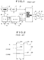
- Fig. 1 a block diagram of the video camera in which the conventional analog signal processing unit is designed in a digital system.
- a sensor 1 in response to an input optical signal, a sensor 1 produces an analog pixel signal 12, for each horizontal read scanning period, which is synchronous with a read clock frequency (hereinafter referred to a sensor clock as) and consisting of repeated alternately different color signals.
- the operation of the sensor 1 is controlled by the control signal sent from the sensor driving timing generating circuit (hereinafter abbreviated to TG).
- the analog pixel signal 12 is A/D converted by an analog/digital converter (hereinafter abbreviated to A/D) to provide a digital pixel signal 13.
- a digital signal processing circuit 3 when it receives the digital pixel signal 13, a synchronization (sync) signal 20 and a control signal 23 from a synchronization signal generating circuit (hereinafter abbreviated to SSG) and the control signal 18 from TG 5, produces a luminance signal 14 and a color signal 15 supplemented with the sync signal 20 supplemented with the sync signal 20, respectively.
- These signals 14 and 15 are D/A converted by a digital/analog converter (abbreviated to D/A) to provide an analog luminance signal 16 and an analog color signal supplemented with the sync signal, respectively.
- SSG 8 when the signal 60 at a frequency of n ⁇ fsc is supplied as a clock from an oscillator 61 with an oscillation frequency of n ⁇ fsc (n: an integer; and fsc: the frequency of a color subcarrier), produces a horizontal sync signal (hereinafter referred to as CHD) and a vertical sync signal (hereinafter referred to as VD) which are necessary to generate a sensor driving signal; these two signals 19 are supplied to TG5.
- CHD horizontal sync signal
- VD vertical sync signal
- TG5 In response to the signal fs from an oscillator 51 and CHD, TG5 produces a sensor clock fs.
- SSG 8 in response to the clock signal at nfsc, SSG 8 produces synchronization (sync) signals 20 such as a composite sync signal (CSYNC), a composite blanking signal (CBLK), a burst flag signal (BF), etc.
- the digital signal processing circuit 3 in response to the sensor clock nfsc, produces the luminance signal and a color difference signal supplemented with the sync signals 20 to provide the luminance signal 14 and the color signal 15 (which is further modulated by the control signal 23), respectively.
- the art related to the system described above is disclosed in Japanese Patent Publication No. 63-45153.
- the present CCD sensor adopts several values as the number of horizontal pixels. Since the horizontal scanning period is fixed, there are different frequencies of horizontal pixel read clock (sensor clock) corresponding to the number of pixels.
- the sensor clock frequency (fs) for an NTSC color television system includes the values of 9.5 MHz, 12.7 MHz, 14.3 MHz, etc.
- the signal processing in the digital camera is desired to be performed in a processing synchronous with the sensor clock because of its easiness and merit of small-sized circuit.
- the signal processing in the encoder must be done with the clock n (n : 3 or 4) times as large as fsc.
- the prior art shown in Fig. 1 has also the following defect.
- no consideration on taking synchronization of a luminance signal with a sync signal when the luminance signal is supplemented with the sync signals is made although the luminance signal is synchronous with the sensor clock fs and the sync signals such as CSYNC are synchronous with n ⁇ fsc.
- Fig. 2 is a timing chart showing the relationship between the sensor clock fs, and CSYNC before it is added to the luminnance signal and CSYNC after it has been added thereto.
- CSYNC is latched at the rising edge 104 so that it remains unvaried and the waveform 102 after added to the luminance signal; on the other hand, CSYNC is latched at not the rising edge 104 but the rising edge 105, SYNC after added to the luminance signal has the waveform 103.
- the timing difference between CSYNC 102 and CSYNC 103 in their falling edge is 1/fs.
- Such a large timing difference will produce jitter in the output image visible to human eyes.
- the video camera cannot deal with the sensor fixed at a different clock frequency; the video camera does not have sufficient versatility.
- An object of the present invention is to provide a video camera with its all the signal processings digitized including that in an encoder which can put within a permitted range (35 ns or less) the jitter generated when 4 fsc is used as the data processing clock in the encoder, and is suitable to implement its low power consumption and small-size/light weight.
- Another object of the present invention is to provide a video camera comprising a digital signal processing circuit which prevents jitter from being generated on an output image, and a programmable SSG which is controlled by a microcomputer to make the timing of the sync signal variable thereby dealing with sensors having several specifications.
- a sync signal generating circuit (SSG) is provided to comprise an nfsc unit for generating a horizontal sync signal and a vertical sync signal for a sensor using the signal at the frequency of nfsc as a clock and a fs unit for generating the sync signal for generating a television signal.
- Another arrangement comprises a signal switching circuit for alternately supplying the sync signals for the luminance signal and the television to the D/A converter means and a clock switching circuit for alternately supplying the clock at the frequency nfsc and the sensor clock fs as a clock for the D/A converter.
- Still another arrangement comprises a programmable SSG which can change the timing of the sync signal for the television generated by the fs unit in order to deal with several sensors and a microcomputer for controlling it.
- the control circuit detects the phase relationship between the phase reference signal and the 4 fsc clock with accuracy of (8 fsc) ⁇ 1 by detecting it at the rising edge and falling edge of the 4 fsc clock, and the phase correction circuit detects the amount of jitter due to the detected phase relationship to replace the color difference signals having the jitter supplied from the data clock converter means by the data interpolated from adjacent data before and after latch, thus making the phase correction for the color difference signals.
- the ratio of the adjacent data to be added can be changed to create the data in any phase. Therefore, the accuracy of phase correction depends on the detection accuracy so that the amount of jitter remaining after the phase correction is equivalent to the detecting accuracy.
- the amount of jitter of the color difference signals after the phase correction is equal to (8 fsc) ⁇ 1 which is within a permissible range for the color signal. In this way, the problem of jitter occurring in the digital encoder can be solved.
- the nfsc unit when the clock at the frequency of nfsc is supplied, the nfsc unit performs a timing generating processing by a counter, etc., to generate a horizontal sync signal (CHD) and a vertical sync signal (VD) for the video camera which are to be supplied to TG.
- TG generates a sensor clock fs using a signal synchronous with CHD and supplies several kinds of control signals including the sensor clock fs to the digital signal processing circuit and the fs unit in SSG.
- the digital signal processing circuit performs a signal processing using the sensor clock fs as a clock to generate the luminance signal and the color difference signal.
- the fs unit uses the sensor clock fs as a clock, the fs unit also generates the sync signals such as a composite sync signal (CSYNC) for a television. Therefore, the luminance signal and the sync signals are synchronous with the sensor clock fs so that the luminance signal is synchronous with the sync signals.
- CSYNC composite sync signal
- the signal switching circuit is switched on the side of the sync signals and also the clock switching circuit is switched on the side of the nfsc so that the sync signals are supplied, using the nfsc clock, to the D/A converter circuit from which analog sync signals are produced.
- the signal switching circuit and the clock switching circuit are switched on the sides opposite to the above cases so that an analog luminance signal is produced from the D/A converter circuit. Therefore, even if the luminance signal and the sync signals are not synchronous with each other at the points A and B, because of the level of the luminance signal being fixed, no jitter is generated.
- the fs unit processes the value of a counter using the sensor clock fs as a clock and the timing data held in the state holding circuit thereby to generate a horizontal sync signal and synthesizes the horizontal sync signal and the vertical sync signal supplied from the nfsc unit, thereby generating sync signals.
- the timing data supplied from the microcomputer to the fs unit are set for the specification of a sensor used, the sync signals applied to the sensor can be generated, thereby realizing versatility for plural sensors.
- Fig. 3 shows the arrangement of the video camera according to one embodiment of the present invention.
- numeral 1 denotes a solid state camera element (sensor);
- numeral 2 denotes an A/D converter;
- numeral 3 denotes a digital signal processing circuit for generating a luminance signal and a color signal;
- numeral 5 denotes a driving circuit (sensor driving timing generating circuit);
- numeral 8 denotes a sync signal generating circuit;
- numerals 4 and 4' denote a D/A converter, respectively.
- the digital signal processing circuit 3 is composed of a data clock converter circuit 42, a phase correction circuit 43, an encoder 44 and a control circuit 45.
- the sync signal circuit 8 generates sync signals (a horizontal/vertical sync signals, a sub-carrier, clocks, etc.) required for a signal processing circuit 41, the driving circuit 5 and other circuits.
- the pulses or the like necessary for the processings in the signal processing circuit 41, an encoder 44 are not shown in Fig. 3 since they are not indispensable to the present explanation.
- the driving circuit 5 reads signals from the solid-state image sensor 1 at the sensor clock cycle fs in synchronism with the horizontal sync signal and the vertical sync signal supplied from the sync signal generating circuit 8.
- the sensor output which corresponds to an optical signal 11 is read from the solid-state image sensor 1 is supplied to the A/D converter 2.
- the A/D converter 2 covnerts the sensor output signal for each pixel into a digital signal in synchronism with the sensor clock; this digital signal is supplied to the signal processing circuit 41.
- the signal processing circuit 41 processes the digital sensor output signal after A/D conversion (which is supplied from the A/D converter 2 through the processing disclosed in Japanese Patent Publication No. 63-45153) on the basis of the sensor clock thereby to produce a luminance signal and color difference signals.
- the color difference signals (R-Y) and (B-Y) thus produced are supplied to the data clock converter circuit 42.
- the control circuit 45 detects with accuracy of (8 fsc) ⁇ 1 a phase difference between the phase reference signal indicative of the changing point of the color difference signals supplied from the signal processing circuit 41 (e.g.
- the data clock converter circuit 42 latches the color difference signals (R - Y) and (B - Y) supplied from the control circuit 45 with the data latch clock so that the color difference signals after latch are sent to the phase correction circuit 43.
- the phase correction circuit 43 phase-corrects the color difference signals (R - Y) and (B - Y) to be sent to the encoder 44.
- the above control circuit 45 latches the supplied phase reference signal at the rising and falling edges of the 4 fsc clock to detect in which period of 'H' and 'L' of the 4 fsc clock the changing points of the color difference signals are located on the basis of the latched two phase reference signals and supplies the detected signal to the phase correction circuit 43.
- control circuit 45 processes the phase reference signal with the 4 fsc clock to generate the latch pulse which will be supplied to the data clock converter circuit 42. It should be noted that this latch pulse can provide a jitter up to (4 fsc) ⁇ 1 to the above phase reference signal in accordance with the phase relationship between the phase reference signal and the 4 fsc clock.
- the data clock converter circuit 42 latches the color difference signals (R - Y) and (B - Y) supplied from the signal processing circuit 41 with the latch pulse supplied from the control circuit 45.
- the latched color difference signals (R - Y) and (B - Y) can be processed using the signal of the 4 fsc clock.
- the latch pulse provides the jitter up to (4 fsc) ⁇ 1 so that the latched color difference signals also have the jitter up to (4 fsc) ⁇ 1.
- the latched color difference signals are further supplied to the phase correction circuit 5.
- the phase correction circuit 43 first latches the color difference signals having the jitter up to (4 fsc) ⁇ 1 supplied from the data clock converter circuit 42 with the above latch pulse and adds these latched color difference signals to the signals before latch supplied from the data clock converter circuit 45 to generate the color difference signals having an intermediate phase.
- the color difference signals having the intermediate phase corresponding to one clock of (4 fsc) ⁇ 1 are selectively produced only if they are located, at the changing points, on the phase side in which the delay time of the color difference signals is shortened owing to latching by the data clock converter circuit 42 in the 'H' side or 'L' side of the 4 fsc clock; and in the other case, the color difference signals supplied from the data clock converter circuit 45 are produced.
- Fig. 4 shows the waveform charts for explicitly explaining the manner of reducing the jitter on the basis of the above processing.
- Fig. 4 shows the state where the maximum jitter is provided assuming that the sensor clock is fs ⁇ (4 fsc) x (2/3), the data cycle of the color difference signal is fs/2, the phase reference signal 13 has substantially the same phase as the 4 fsc clocks 15 and 16 (the phases A and B are slightly earlier and later from the phase reference signal 13, respectively).
- a waveform 12 denotes a sensor clock fs; a waveform 13 denotes the phase reference signal; a waveform 14 denotes the color difference signals; the waveform 15 denotes the 4 fsc clock when its rising edge is in the phase (A phase) slightly earlier than that of the phase reference signal 13; the waveform 16 is denotes the 4 fsc clock in the phase (B phase) slightly later than that of the phase reference signal 13; a waveform 17 denotes the data latch clock corresponding to the phase A, a waveform 18 denotes the data latch clock corresponding to the phase B; a waveform 19 denotes the color difference signals after latch corresponding to the phase A; a waveform 20 denotes the color difference signals after latch corresponding to the phase B; and a waveform 21 denotes the color difference signals phase-corrected corresponding to the phase B.
- the data latch clocks 17 and 18 are generated by twice latching the phase reference signal with the rising edge of the 4 fsc clock. The reason for this is that generally, if the latched data and the latched clock are completely in phase with each other, the latched data may be unstable so that the malfunction due to this should be prevented. However, whether or not the jitter occurs owing to latching depends on the first latching. As mentioned above, the phase of the phase reference signal is decided according to which period of 'H' (a in Fig. 4) and 'L' (b in Fig. 4) of the 4 fsc clock its rising edge is located on.
- the control circuit 45 detects the phase B and the detected signal is supplied to the phase correction circuit 43.
- the phase correction circuit executes the phase correction only at the phase B to produce the color difference signals after phase correction as shown by the waveform 21.
- the color difference signals as shown by the waveform 19 are used as they are.
- the above processing provides the jitter of (8 fsc) ⁇ 1 corresponding to the phase difference between the center points (C A and C B ' in Fig.
- the above processing can reduce the jitter up to (4 fsc) ⁇ 1 to (8 fsc) ⁇ 1.
- the jitter attendant on the data clock conversion of the color difference signals (R - Y) and (B - Y) to be supplied to the encoder 44 can be limited to (8 fsc) ⁇ 1 or less.
- the encoder 44 balanced-modulates the supplied color difference signals (R - Y) and (B - Y) using the 4 fsc clock and fsc clock supplied from the sync signal generating circuit 8.
- the modulated color signal generated through the above processing and the luminance signal produced by the signal processing circuit 41 are sent to D/A converter circuits 4' and 4, respectively.
- the D/A converters circuits 4 and 4' convert the supplied luminance signal and modulated color signal into corresponding analog signals, respectively. These D/A converter circuits 4 and 4' are not required if the above luminance signal and modulated color signal are processed hereafter as they are digital signals.
- the signal processing including an encoder can be digitized, and when the sensor having any number of pixels is used, the jitter generated in the encoder can be limited to (8 fsc) ⁇ 1, thus preventing the image quality from changed.
- Fig. 5 shows the respective details of the data clock converter circuit 42, the phase correction circuit 53 and the control circuit 45.
- Fig. 6 shows the waveforms at the respective points in Fig. 5. As described in connection with Fig. 4, in Fig. 6 also, assuming that the sensor clock is fs ⁇ (4 fsc) x (2/3), and the phase reference signal and the edge of the 4 fsc clock are substantially in phase with each other, the state providing the maximum amount of jitter is taken. Further, it is also assumed that the data cycle of the color difference signals (R - Y) and (B - Y) is 1/2 of the sensor clock as in the previous case.
- the data clock converter circuit 42 is composed of latch circuits 422 and 423; the phase correction circuit is composed of latch circuits 530, 531, adder circuits 532, 533, coefficient circuits 534, 535, multiplexers 536, 537, a DFF (D flip-flop) 538, a NOR gate 539 and an AND gate 540; and the control circuit 45 is composed of DFF's 454, 455, 456, 457 and 458 and an inverter 459. Further, in Fig. 6, the same reference numerals refer to the same waveforms in Fig. 4.
- the waveform 13 denotes a phase reference signal
- the waveform 14 denotes a data train Di resulting from the sum of i-th (R - Y) and (B - Y)
- the waveform 15 denotes the 4 fsc clock having the phase (A phase) that is slightly earlier than the rising edge of the phase reference signal
- the waveform 16 denotes the 4 fsc clock having the phase (B phase) that is slightly later than the phase reference signal 13.
- the other waveforms correspond to like waveforms in Fig. 4.
- phase reference signal 13 and the 4 fsc clock are supplied to the control circuit 45.
- the control circuit 45 latches the supplied phase reference signal (waveform 13) twice at the rising edge of the 4 fsc clock by DFF's 454 and 455 and twice at the falling edge of the 4 fsc clock by DFF's 456 and 457.
- the respective Q outputs of DFF 454 and 456 provide pairs of waveforms 17 (phase A) and 18 (phase B), and 50 (phase A) and 51 (phase B).
- the Q output from the DFF 454 is supplied to the data clock converter circuit 42 and the phase correction circuit 53 as a data latch clock.
- the Q output from DFF 456 is further latched by DFF 458 with the Q output from DFF 454.
- the Q output from DFF 458 provides the waveform 52 in the phase A and the waveform 53 in the phase B. Therefore, according as the Q output from DFF 458 is 'L' or 'H', it is possible to detect in which period of the 'H' (a in Fig. 6) and 'L' (b in Fig. 6) periods of the 4 fsc clock the rising edge of the phase reference signal 13 is located. This operation corresponds to the phase detection described previously.
- the Q output from DFF 458 is supplied to the phase correction circuit 53 as a phase detection signal.
- the data clock converter circuit 42 latches the color difference signals (R - Y) and (B - Y) indicated by numeral 14 by the latch circuits 422 and 423 with the data latch clock supplied from the control circuit 45.
- Each of the latch circuits 422 and 423 may be composed of DFF's corresponding to the number of bits of the color difference signals (R - Y) and (B - Y).
- the respective outputs of the latch circuits 422 and 423 provide the waveform (phase A) or the waveform (phase B). These output signals are supplied to the phase correction circuit 53.
- the phase correction circuit 53 latches the color difference signals (R - Y) and (B - Y) supplied from the data clock converter circuit 42 by the latch circuits 530 and 531 with the data latch clock supplied from the control circuit 45.
- the color difference signals (R - Y) and (B - Y) after latch are added to the color difference signals before latch supplied from the data clock converter circuit 42.
- the signals thus obtained are multiplied by the coefficient circuits 534 and 535 to provide the color difference signals (D i + D i+1 )/2 in the intermediate phase between D i and D i+1 which are supplied to the multiplexers 536 and 537.
- the multiplexers 536 and 537 produce the supplied color difference signals in the intermediate phase and the color difference signals supplied from the data clock inverter circuit 42 in accordance with the output signal from the AND gate 540. Now it is assumed that if the output form the AND gate 540 is 'H', the color difference signals in the intermediate phase are produced. On the other hand, the rising edge detecting circuit composed of DFF 538 and NOR gate 539 produces an edge signal which is 'H' during only one cycle of the 4 fsc clock immediately after the supplied data latch clock has changed from 'L' to 'H'.
- the AND gate 540 in accordance with the phase detection signal supplied from the control circuit 45, supplies the above edge signal to the multiplexers 536 and 537 for the phase B and mask this signal for the phase A.
- the waveform of the output from the AND gate 540 is shown as the waveforms 54 (phase A) and 55 (phase B) in Fig. 6.
- the multiplexers 36 and 37 selectively produces the color difference signals in the intermediate phase only at the edge of the phase B, and produce the color difference signals having the waveform 19 for the phase A and those having the waveform 21 for the phase B. These color difference signals are those with the jitter suppressed.
- Fig. 7 shows the details of the digital encoder 44 in an NTSC system in Fig. 3.
- the digital encoder 44 is composed of latch circuits 441, 442, polarity inverter circuits 445, 446, DFF's 443, 444, and an adder 447.
- the operation of the digital encoder 44 will be explained below.
- the color subcarrier fsc having the waveform 66 supplied from the sync signal generating circuit 8 (Fig. 3) is latched by the DFF 433 with the 4 fsc clock having the waveform 65.
- a signal having the waveform 67 is obtained.
- this signal is latched by DFF 444 to provide a signal having the waveform.
- the signals having the waveforms 67 and 68 thus obtained are color subcarrier signals having a phase difference of 90° from each other, which are supplied to the polarity inverter circuits 445 and 446.
- the polarity inverter circuits 445 and 446 if the signals from DFF's 443 and 444 are 'L', invert the polarities of the color difference signals (waveforms 69 and 70) which have been obtained by latching the color difference signals with the jitter suppressed by the phase correction circuit with the 4 fsc clock, thus producing signals having waveforms 70 and 71.
- Fig. 9 shows another embodiment of the present invention.
- like reference numerals designate like components in the previous embodiment.
- the present embodiment uses both 8 fsc clock and 4 fsc clock to detect the changing points of the color difference signals with the accuracy of (16 fsc) ⁇ 1 for phase correction.
- the jitter generated results in (16 fsc) ⁇ 1.
- the maximum frequency of the clock is twice as large as in the embodiment of Fig. 3 and so the power consumption of the oscillator is increased.
- the data processing is performed using the clock up to 4 fsc so that the power consumption in the data processing is substantially equal to that in the previous embodiment.
- the embodiment shown in Fig. 9 is basically different from the previous embodiment in only its phase correction circuit 43' so that only the phase correction circuit 43' will be explained below referring to Fig. 10.
- the control circuit 45' divides one cycle of the 4 fsc clock into four parts to detect in which range the changing points of the color difference signals (rising phase of the phase reference signal) are changed.
- the phase ranges divided into four parts are designated by a, b, c and d in Fig. 10.
- the cases where the rising edges of the phase reference signal are located in a, b, c and d are referred to as phases A, B, C and D, respectively.
- Waveforms 72 and 73, waveforms 74 and 75, waveforms 76 and 77 and waveforms 78 and 79 are the 4 fsc clock and the 8 fsc clock in the cases of phases A, B, C and D, respectively.
- waveforms 80, 81, 82 and 83 are data latch clocks, corresponding to the respective phases, produced by latching the phase reference signal 13 with the rising edge of the 8 fsc clock and thereafter with that of the 4 fsc clock.
- the phase A, the phase B and the phase C are earlier than the phase D by (16 fsc) ⁇ 1, 2 (16 fsc) ⁇ 1 and 3 (16 fsc) ⁇ 1, respectively. Therefore, the color difference signals latched by the data clock converter circuit 42 with these data latch clocks have the above phase differences corresponding to the respective phases.
- the phase correction circuit 43 creates, on the basis of the color difference signal (D i-1 , D i ), the signals having intermediate phases (1/4 D i-1 + 3/4 D i ), (1/2 D i-1 + 1/2 D i ) and (3/4 D i-1 + 1/4 D i ) and outputs these signals having the intermediate phases corresponding to the phases A, B and C during only one cycle of the 4 fsc clock at the changing points of the color difference signal, thus providing waveforms 84, 85, 86 and 87 the center points of which are out of phase from one another as designated by C A , C B , C C and C D .
- the jitter can be corrected with high accuracy of (16 fsc) ⁇ 1.
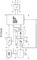
- the video camera system is composed of a sensor 1, an analog/digital converter circuit (A/D) 2, a digital signal processing circuit 3, a digital/analog circuit (D/A) 4, a sensor driving timing generating circuit (TG) 5, an oscillation circuit 51, a sync signal generating circuit (SSG) 6 and an oscillation circuit 61.
- A/D analog/digital converter circuit
- D/A digital/analog circuit
- TG sensor driving timing generating circuit
- SSG sync signal generating circuit
- the sensor 1 when having received an optical signal 11, produces for each one horizontal scanning period an analog pixel signal 12 composed of repeated color signals which are synchronous with the sensor clock at the frequency of fs and alternately different.
- the operation of the sensor 1 is controlled by the control signal 18 from the TG 5.
- the A/D 2 when it receives the analog pixel signal from the sensor 1, converts it into a digital pixel signal 13 which is in turn supplied to the digital signal processing circuit 3.
- the digital signal processing circuit 3 when it receives the digital pixel signal 13 from the A/D 2, the control signal 18 from the TG 5, and the sync signal 20 and control signal 23 from SSG 6, produces a luminance signal 14 and a color signal 15 supplemented with the sync signal, respectively which are supplied to the D/A 4.
- the D/A 4 when it receives the luminance signal 14 and the color signal 15 supplemented with the sync signal, converts these two signals 14 and 15 into analog signals to produces a luminance signal 16 and a color signal 17 supplemented with the analog sync signal, respectively.
- the SSG 6 creates the sync signal 20 on the basis of the control signal 20.
- the TG 5 creates the control signal 18 on the basis of the control signal 19 sent from the SSG 6 and the reference signal 50 sent from the oscillation circuit 51.
- Fig. 12 shows an concrete arrangement of the SSG 6.
- the SSG 6 is composed of an n fsc unit 63 and a fs unit 63.
- the n fsc unit 62 is composed of a horizontal sync signal generating circuit 621 and a vertical sync signal generating circuit 622
- the fs unit is composed of a horizontal sync signal generating circuit 633 and a sync signal creating circuit 635.
- the horizontal sync signal generating circuit 621 when the n fsc unit 62 receives the signal 60 at the frequency of n fsc from the oscillation circuit 61, the horizontal sync signal generating circuit 621 generates a horizontal sync signal 623 which is sent to the vertical sync signal generating circuit 622.
- the vertical sync signal generating circuit 622 when it receives the horizontal sync signal 623 from the horizontal sync signal generating circuit 621, generates a vertical sync signal 625 which is supplied to the sync signal creating unit 635 in the fs unit 63.
- the n fsc unit 62 sends to the TG 5, as the control signals 19, the signal (CHD) 624 for creating the signal horizontally driving the sensor 1 in the horizontal sync singal 623 and the signal (VD) 626 for creating the signal vertically driving the sensor 1 in the vertical sync signal 625.
- the TG 5, which receives the control signals 19 from the SSG 6, takes the phase lock of the signal obtained by frequency-dividing the reference signal 50 supplied from the oscillation circuit 50 with the CHD 624 and creates the control signals such as the sensor clock at the frequency of fs from the above reference signal 50; the control signals 18 are sent to the fs unit 63 in the SSG 6.
- the horizontal sync signal generating circuit 633 when it receives the control signals 18, generates a horizontal sync signal 638 synchronous with the sensor clock fs which is supplied to the sync signal creating circuit 635.
- the sync signal creating circuit 635 when it receives the vertical sync signal 625 from the vertical sync signal generating circuit 622, the horizontal sync signal 638 from the horizontal sync signal generating circuit 633, creates sync signals (CSYNC, CBLK, BF) 20 which are supplied to the digital signal processing circuit 3. It should be noted that the horizontal sync signal 638 and the vertical sync signal 625 are synchronous with the sensor clock fs so that the sync signals are also synchronous with the sensor clock fs.
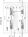
- Fig. 13 shows a concrete arrangement of the digital signal processing circuit 3.
- the digital signal processing circuit 13 is composed of a Y/C separation circuit 31, a Y process circuit 32, a C process circuit and a CSYNC supplementing circuit 34, a BF supplementing circuit 35 and a modulation circuit 36.
- the operation of the digital signal processing circuit 3 will be explained below.
- the Y/C separation circuit 31 when it receives the digital pixel signal 13 from the A/D 2, creates the first pixel signal which is a luminance signal obtained by extracting the luminance component from the output signal from the A/D 2, and the second pixel signal 302 which is a color signal also extracted from the output signal from the A/D 2; these two signals are supplied to the Y process circuit 32 and the C process circuit 33, respectively.
- the Y process circuit 32 when it receives the first pixel signal 301 and the second pixel signal 302 from the Y/C separation circuit 31, creates a luminance signal 313 to be supplied to the CSYNC supplementing circuit 34.
- the C process circuit 33 when it receives the first pixel signal 301 and the second pixel signal 302 from the Y/C separation circuit 31, creates color difference signals 304 to be supplied to the BF supplementing circuit 35.
- the Y/C separation circuit 31, the Y process circuit 32 and the C process circuit 33 which are controlled by the control signals 18 supplied from the TG 5, are phased-locked with the sensor clock fs. Therefore, the luminance signal 303 and the color difference signals 304 are also synchronous with the sensor clock fs, respectively.
- the sync signals supplied from the SSG 6 include three signals of CSYNC 305, CBLK 306 and BF 307.
- the CSYNC supplementing circuit 34 when it receives the luminance signal 303 from the Y process circuit 32, and CSYNC 305 and CBLK 306 from the SSG 6, creates the luminance signal 14 supplemented with the sync signals 20.
- the BF supplementing circuit 35 when it receives the color difference signals 304 from the C process circuit 33, and BF 305 and CBLK 306 from the SSG 6, creates the color difference signals 308 supplemented with the sync signals; the color difference signals are supplied to the modulation circuit 36.
- the modulation circuit 36 when it receives the color difference signal supplemented with the sync signals from the BF supplementing circuit 35 and the control signal 23 from the SSG 6, the color signal 15 supplemented with the sync signals. Thereafter, the D/A 4 converts the luminance signal 14 and the color signal 15 supplemented with the sync signals into the analog luminance signal 16 and the analog color signal 17, respectively.
- the signal processing is controlled by the sensor clock and the sync signals are also created on the basis of the sensor clock so that the digital luminance signal is made synchronous with the sync signals; thus, it is possible to prevent the jitter from being generated in synthesizing the above two signals.
- Figs. 14 to 17 a modification of this embodiment will be explained below.
- the basic arrangement of video camera system according to this modification is substantially the same as that shown in Fig. 11, but is different from the latter in that the SSG 6 is repalced by a programmable SSG 65 and a microcomputer 7 for controlling it is provided.
- Fig. 14 shows a concrete arrangement of the programmable SSG 65 and the microcomputer 7.
- the SSG 65 is composed of an n fsc unit 62 and a fs unit 64; the fs unit is composed of a counter 631, a latch circuit 632, a horizontal sync signal generating circuit 634 and a sync signal creating circuit 635.
- the n fsc unit 62 and the sync signal creating circuit 635 are entirely the same as those in the SSG 6 in Fig. 12.
- Fig. 15 shows the details of each block in the fs unit 64. In Fig.
- the latch circuit 632 is composed of latch circuits 632a and 632b
- the horizontal sync signal generating circuit 634 is composed of a comparator circuit 634a and a pulse generating circuit 634b.
- a signal 22 denotes timing data including a data 22a and an address 22b
- signals 639 and 640 denote output signals from the comparator 634a
- a signal 638 denotes a horizontal sync signal.
- Fig. 16 shows a timing chart for explaining the process of creating the horizontal sync signal 638. With reference to Figs. 14 to 16, the operation of the SSG 65 and the microcomputer 7 will be explained below.
- the microcomputer 7 sends to the latch circuit 632 the timing data (set as a and b in the microcomputer 7) for creating the sync signals adapted to the specification of the sensor 1 whereby the data 22a is latched in the latch circuit 632.
- the latch circuit (632a or 632b) in which the data 22a should be latched is determined in accordance with the address 22b. Now it is assumed that a value a is held in the latch circuit 632a while a value (a + b) is held in the latch circuit 632b.
- the values a and (a + b) are two points apart from a time b.
- the sync signal with a synchronization b can be generated. Namely, if the values a and b are set as input data for the microcomputer 7, a programmable SSG can be realized.
- the counter 631 when it receives the control signal 18 from the TG 5, counts the sensor clock fs (number of clocks); the counted value 636 is supplied to the comparator circuit 634a in the horizontal sync signal generating circuit 834.
- the comparator circuit 634a when it receives timing data 637a and 637b from the latch circuit 632 and the counted value 636 from the counter 631, examines if the counted value 636 coincides with the timing data 637a or 637b, and outputs '1' or '0' in accordance with the absence or presence of the coincidence. Namely, the comparator circuit 634a produces signals 639 and 640 in the timing chart of Fig. 16.
- the pulse generating circuits 634b when it receives the signals 639 and 640, generates the sync signal 638 as shown in Fig. 16 which is in turn sent to the sync signal creating circuit 635.
- the sync signal creating circuit 635 when it receives the vertical sync signal 625 from the vertical sync signal generating circuit 622 and the horizontal sync signal 638 from the horizontal sync signal generating circuit 634, creates sync signals including CSYNC, CBLK and BF which are in turn sent to the digital signal processing circuit 3.
- the succeeding operation is the same as in the embodiment of Fig. 11.
- a plurality of latch circuits 632 connected in series with a plurality of pulse generating circuits 634 may be arranged in such a manner that signal input/output switches SW1 and SW2 are synchronously connected with any series connection of these latch circuits and pulse generating circuits, thereby providing a plurality of horizontal sync signals defined by series connections of the latch circuits 632 and the pulse generating circuit 634.
- the latch circuit 632 may be replaced by any component as long as it has a state holding function.
- the programmable SSG and the microcomputer for controlling it are provided so that the timing of the horizontal sync signal can be made variable. Therefore, the sync signal adapted to the sensor to be used can be generated so that the video camera can deal with a plurality of kinds of sensors.
- the basic arrangement of the video camera system according to this embodiment is substantially the same as that in Fig. 11 except the arrangement of Fig. 18.
- the operation of each of the respective blocks is also the same as that of each of the corresponding blocks in Fig. 11.
- the video camera according to this embodiment is characterized by the provision of a programmable TG 9 and a microcomputer 7 for controlling it.
- the programmable TG 9 when it receives the timing data 22 from the microcomputer 7 and the sync signals from the SSG 6, a necessary timing control signal by the same latch circuit and pulse generating circuit as those included in the fs unit 64 in the programmable SSG 65 in Fig. 14.
- the sensor driving pulse and the control signal for signal processing can be changed in accordance with the kind of the sensor and the system arrangement.
- FIG. 19 shows the basic arrnagement of the video camera system according to this embodiment.
- This video camera is composed of a sensor 1, an A/D 2, a digital signal processing circuit 3, a D/A 4, a TG 52, a programmable SSG 6, a control circuit 10 and an oscillation circuit 51.
- the oscillation circuit 51 supplies a reference signal 50 to the TG 52.
- the TG 52 when it receives the reference signal 50 from the oscillation circuit 51, frequency-divides the reference signal 50 to create a control signal 19 such as the sensor clock fs and a sensor driving signal 181 for driving the sensor 1 which are in turn sent to the programmable SSG 66 and the sensor 1, respectively.
- the programmable SSG 66 comprises the same circuits as the fs unit 64.
- the programmable SSG 6 when it receives the timing data 22 for generating the sync signals adapted to several sensors from the exterior and the control signal 191 such as the sensor clock fs from the TG 52, creates the sync signals 20 synchronous with the sensor clock fs and the control signals 25 which are in turn sent to the digital signal processing circuit 3 and the control circuit 10, respectively.
- the control circuit 10 when it receives the control signals from the programmable SSG 66, supplies the control signals such as a clock to the A/D 2, and supplies the control signals such as the sensor clock fs to the digital signal processing circuit 3.
- the video camera system according to this embodiment produces the analog luminance signal and color signal supplemented with the sync signals through the same process as in video camera system according to the embodiment of Fig. 11.
- the programmable SSG 66 which can generate sync signals at different timings on the basis of data (information such as a and b required to create sync signals) externally supplied so that the video camera can deal with a plurality of kinds of sensors.
- FIG. 19 The basic arrangement of the video camera according to this embodiment is that of Fig. 19 further provided with a microcomputer 7 and an input terminal 71 for data rewrite.
- the microcomputer 7 temporarily holds data 72 inputted through the terminal 71 and further supplies the data 72 to the programmable SSG 66 as the timing data 22 to rewrite the timing data held in the SSG 6.
- the data 72 should be not limited to the timing data 22 and the microcomputer 7 can execute not only the above operation but also control the other circuits as required using the data 72.
- the arrangement of Fig. 19 may be provided with a ROM 73.
- the data can be supplied from the ROM 73 to the microcomputer 7.
- the programmable SSG 6 can generate the sync signals adapted to the used sensor using the timing data supplied from the microcomputer so that the video camera system according to this embodiment can deal with a plurality of sensors.
- the video camera can be automatically set up in its start.
- Fig. 22 may be modified into that as shown in Fig. 23.
- the data timing data 22 which is part of the data stored in the ROM 73 is directly supplied to the programmable SSG 66.
- a microcomputer 70 stores several kinds of timing data corresponding to individual systems, and a programmable ROM 74 stores the codes allotted to the respective systems and control data.
- a system selection data 78 is supplied to the microcomputer 70 through an input terminal 76.
- the microcomputer 70 when it receives the system selection data 78, reads, from the programmable ROM 74, system data 77 including the code designated by the selection data 78 and the control data, and supplies to the programmable SSG 66 the timing data 22 designated by the above code of several kinds of timing data stored in the microcomputer 70. And the control data is further supplied to the control circuit 10.
- the other operations are the same as those of the video camera system in the embodiment of Fig. 19.
- the system selection data has only to be supplied from the input terminal 76 to automatically place the video camera system in a normally operable state, thereby improving the working efficiency in the production process.
- Figs. 20A, 20B and 21 an explanation will be given of a further modified embodiment of Fig. 11.
- the basic arrangement of the video camera system according to this embodiment is substantially the same as the prior art shown in Fig. 1.
- the digital signal processing circuit 3 is also substantially the same as that in Fig. 13 except the arrangement of the luminance signal processing unit 37 encircled by a dotted line.
- Fig. 20A shows a circuit for supplying the luminance signal and sync signals to the D/A converter unit 4.
- This luminance signal processing circuit is composed of a signal switch 371 and a clock switch 372.
- Fig. 21 shows the waveform of the luminance signal supplemented with sync signals. Since the basic operation of the video camera according to this embodiment is substantially the same as that of the prior art shown in Fig. 1 except the D/A conversion operation, only the operation of the luminance signal processing unit 37 will be explained.
- the signal switch 371 connects a terminal 375 with a terminal 374 to supply the sync signals 20 to the D/A converter unit 4, and the clock switch 372 connects a terminal 377 with a terminal 378 to the n fsc clock to the clock terminal 34 of the D/A converter unit 4. Then, in response to the n fsc clock, the D/A converter unit 4 converts the sync signals into an analog signal to be outputted as in Fig. 20A.
- the signal switch 371 is switched into a terminal 373 to supply the luminance signal 303 to the D/A converter unit 4, and the clock switch 372 is switched into a terminal 376 to supply the sensor clock fs which is one of the control signals to the clock terminal 24 of the D/A converter unit 4.
- the D/A converter unit 4 converts the luminance signal 303 into an analog luminance signal to be outputted.
- Such an operation is continued during the interval B - A' until a time A'.
- the signal switch 371 and the clock switch 372 are switched into opposite terminals, respectively so that the same operation as during the above interval A - B. Thereafter, the above operations will be repeated. It should be noted that in Fig.
- the level of the luminance signal is fixed during all the intervals C, D, C' and D' where the switching timings A, B, A' and B' are located.
- the horizontal blanking signal HBLK as shown in Fig. 20B included in the sync signals 20 is supplied to the signal switch 371 and the clock switch 372 as a switching signal.
- the terminals 375 and 378 are connected with the terminals 374 and 377, respectively whereas at the rising edge of HBLK, the terminals 375 and 378 are connected with the terminals 373 and 376, respectively.
- the luminance signal and the sync signals are D/A converted at the timings at both ends of the horizontal blanking period where the level of the luminance signal is fixed. Therefore, even if the luminance signal is not synchronous with the sync signals, any jitter influencing the out is not generated.
- the jitter theoretically attendant on the digital encoder based on a 4 fsc clock can be limited in a permissible range of (8 fsc) ⁇ 1; thus, the all the signal processing systems including the digital encoder can be digitized with no attenuation of image quality. Accordingly, the video camera system having merits of digitization of low power consumption, compactness, light weight, high image quality, etc. can be realized.
- the sync signal generating circuit is composed of a unit for generating a horizontal sync signal and a vertical sync signal in response to the clock at the frequency K (dependent on a color television) times as large as that of a color subcarrier, and a unit for generating sync signals to be added to a luminance signal and color difference signals, and the luminance signal which is not still supplemented with the sync signals is generated on the basis of the horizontal read clock of the sensor used.
- the luminance signal is made synchronous with the sync signals so that the jitter attendant on the digitization in the signal processing can be removed to realize the high image quality.
- the video camera can be a plurality kinds of sensors, and its versatility and low cost can also be realized.
Landscapes
- Engineering & Computer Science (AREA)
- Multimedia (AREA)
- Signal Processing (AREA)
- Processing Of Color Television Signals (AREA)
- Color Television Image Signal Generators (AREA)
Priority Applications (1)
| Application Number | Priority Date | Filing Date | Title |
|---|---|---|---|
| EP96101752A EP0720389B1 (de) | 1990-10-31 | 1991-10-29 | Zittervermeidung im Videokameraausgabebild |
Applications Claiming Priority (4)
| Application Number | Priority Date | Filing Date | Title |
|---|---|---|---|
| JP2292012A JP2738778B2 (ja) | 1990-10-31 | 1990-10-31 | 撮像装置 |
| JP292012/90 | 1990-10-31 | ||
| JP297299/90 | 1990-11-05 | ||
| JP2297299A JP3009206B2 (ja) | 1990-11-05 | 1990-11-05 | ビデオカメラ装置 |
Related Child Applications (2)
| Application Number | Title | Priority Date | Filing Date |
|---|---|---|---|
| EP96101752A Division EP0720389B1 (de) | 1990-10-31 | 1991-10-29 | Zittervermeidung im Videokameraausgabebild |
| EP96101752.2 Division-Into | 1991-10-29 |
Publications (3)
| Publication Number | Publication Date |
|---|---|
| EP0483745A2 true EP0483745A2 (de) | 1992-05-06 |
| EP0483745A3 EP0483745A3 (en) | 1993-07-14 |
| EP0483745B1 EP0483745B1 (de) | 1997-10-15 |
Family
ID=26558800
Family Applications (2)
| Application Number | Title | Priority Date | Filing Date |
|---|---|---|---|
| EP91118399A Expired - Lifetime EP0483745B1 (de) | 1990-10-31 | 1991-10-29 | Digitale Farbsignal-Verarbeitung mit Taktsignalsteuerung für eine Videokamera |
| EP96101752A Expired - Lifetime EP0720389B1 (de) | 1990-10-31 | 1991-10-29 | Zittervermeidung im Videokameraausgabebild |
Family Applications After (1)
| Application Number | Title | Priority Date | Filing Date |
|---|---|---|---|
| EP96101752A Expired - Lifetime EP0720389B1 (de) | 1990-10-31 | 1991-10-29 | Zittervermeidung im Videokameraausgabebild |
Country Status (4)
| Country | Link |
|---|---|
| US (2) | US5287171A (de) |
| EP (2) | EP0483745B1 (de) |
| KR (1) | KR940005173B1 (de) |
| DE (2) | DE69132577T2 (de) |
Cited By (4)
| Publication number | Priority date | Publication date | Assignee | Title |
|---|---|---|---|---|
| US6295084B1 (en) | 1995-03-10 | 2001-09-25 | Hitachi, Ltd. | System with analog interface and signal processor therefor |
| WO2004068849A1 (en) * | 2003-01-30 | 2004-08-12 | Qualcomm Incorporated | Modular architecture having reusable front end for processing digital video data |
| CN102338628A (zh) * | 2011-08-15 | 2012-02-01 | 中国商用飞机有限责任公司 | 用于测试传感器的信号测试仿真装置 |
| US8131099B2 (en) * | 2006-07-13 | 2012-03-06 | Canon Kabushiki Kaisha | Image processing apparatus and method of controlling image processing apparatus |
Families Citing this family (14)
| Publication number | Priority date | Publication date | Assignee | Title |
|---|---|---|---|---|
| DE69132577T2 (de) * | 1990-10-31 | 2001-11-29 | Hitachi, Ltd. | Zittervermeidung im Videokameraausgabebild |
| JP3696895B2 (ja) * | 1993-06-21 | 2005-09-21 | キヤノン株式会社 | ビデオカメラ及び映像信号処理方法 |
| US5717611A (en) * | 1993-10-08 | 1998-02-10 | Nikon Corporation | Slight motion detecting device |
| US5844629A (en) * | 1996-05-30 | 1998-12-01 | Analog Devices, Inc. | Digital-to-analog video encoder with novel equalization |
| US6580456B1 (en) * | 1997-11-16 | 2003-06-17 | Pictos Technologies, Inc. | Programmable timing generator |
| JP4086354B2 (ja) * | 1998-02-12 | 2008-05-14 | ローム株式会社 | マルチフォーマットビデオエンコーダ |
| JP2000106646A (ja) * | 1998-09-28 | 2000-04-11 | Matsushita Electric Ind Co Ltd | 撮像装置 |
| US6593871B1 (en) | 2000-08-31 | 2003-07-15 | Dalsa, Inc. | Automatic A/D convert positioning circuit and method |
| SE522231C2 (sv) | 2002-04-10 | 2004-01-27 | Axis Ab | Bildalstringsanordning och timinggenerator |
| JP4379380B2 (ja) * | 2005-04-28 | 2009-12-09 | ソニー株式会社 | 水平レジスタ転送パルス生成回路及び撮像装置 |
| JP4271244B2 (ja) * | 2007-03-26 | 2009-06-03 | 株式会社半導体理工学研究センター | アナログ・デジタル(ad)変換器及びアナログ・デジタル変換方法 |
| JP2009188993A (ja) * | 2008-01-07 | 2009-08-20 | Nikon Systems Inc | データ転送装置およびカメラ |
| JP5304280B2 (ja) * | 2009-01-30 | 2013-10-02 | 株式会社ニコン | 位相調整装置およびカメラ |
| KR102238151B1 (ko) * | 2015-03-25 | 2021-04-08 | 한화테크윈 주식회사 | 영상 신호 변환 장치 및 방법 |
Family Cites Families (20)
| Publication number | Priority date | Publication date | Assignee | Title |
|---|---|---|---|---|
| US4038683A (en) * | 1975-04-04 | 1977-07-26 | Rca Corporation | Television synchronizing generator |
| JPS60838B2 (ja) * | 1976-05-28 | 1985-01-10 | ソニー株式会社 | カラー固体撮像装置 |
| JPS55500273A (de) * | 1978-04-10 | 1980-05-08 | ||
| US4345270A (en) * | 1981-01-27 | 1982-08-17 | Sony Corporation | Solid state digital television camera |
| US4620222A (en) * | 1982-11-10 | 1986-10-28 | Matsushita Electric Industrial Co., Ltd. | Digital color TV camera |
| JPS59181884A (ja) * | 1983-03-31 | 1984-10-16 | Matsushita Electric Ind Co Ltd | カラ−カメラ装置 |
| US4654708A (en) * | 1983-06-20 | 1987-03-31 | Racal Data Communications Inc. | Digital video sync detection |
| US4599640A (en) * | 1984-02-29 | 1986-07-08 | Rca Corporation | Television camera with multiplexed A-D converter |
| JPS60214183A (ja) * | 1984-04-09 | 1985-10-26 | Nec Corp | カラ−撮像装置 |
| DE3432314A1 (de) * | 1984-09-03 | 1986-03-13 | Philips Patentverwaltung Gmbh, 2000 Hamburg | Schaltungsanordnung zum ableiten digitaler farbsignale aus einem analogen fernsehsignal |
| US4692889A (en) * | 1984-09-28 | 1987-09-08 | Rca Corporation | Circuitry for calculating magnitude of vector sum from its orthogonal components in digital television receiver |
| US4686567A (en) * | 1984-09-28 | 1987-08-11 | Sundstrand Data Control, Inc. | Timing circuit for varying the horizontal format of raster scanned display |
| US4894794A (en) * | 1985-10-15 | 1990-01-16 | Polaroid Corporation | System for providing continous linear interpolation |
| FR2602112B1 (fr) * | 1986-07-25 | 1988-10-21 | Thomson Video Equip | Procede d'elaboration d'un signal standard de television en couleurs et chaine de prise de vues utilisant ce procede |
| US5045942A (en) * | 1987-11-18 | 1991-09-03 | Nec Corporation | Digital video communication system having a network clock source |
| JPH0236672A (ja) * | 1988-07-27 | 1990-02-06 | Sony Corp | 同期信号発生回路 |
| US5008740A (en) * | 1989-04-14 | 1991-04-16 | North American Philips Corp. | Apparatus and method for creating digitally remodulated video from digital components |
| DE69132577T2 (de) * | 1990-10-31 | 2001-11-29 | Hitachi, Ltd. | Zittervermeidung im Videokameraausgabebild |
| US5138320A (en) * | 1990-11-14 | 1992-08-11 | Zenith Electronics Corporation | Skew code generator for measuring pulses width using a delay line |
| JP3370731B2 (ja) * | 1993-06-02 | 2003-01-27 | キユーピー株式会社 | 押出し容器およびその内容物押出し方法 |
-
1991
- 1991-10-29 DE DE69132577T patent/DE69132577T2/de not_active Expired - Lifetime
- 1991-10-29 US US07/783,995 patent/US5287171A/en not_active Expired - Lifetime
- 1991-10-29 EP EP91118399A patent/EP0483745B1/de not_active Expired - Lifetime
- 1991-10-29 EP EP96101752A patent/EP0720389B1/de not_active Expired - Lifetime
- 1991-10-29 DE DE69127950T patent/DE69127950T2/de not_active Expired - Fee Related
- 1991-10-30 KR KR1019910019099A patent/KR940005173B1/ko not_active Expired - Lifetime
-
1993
- 1993-10-06 US US08/132,309 patent/US5483290A/en not_active Expired - Lifetime
Cited By (6)
| Publication number | Priority date | Publication date | Assignee | Title |
|---|---|---|---|---|
| US6295084B1 (en) | 1995-03-10 | 2001-09-25 | Hitachi, Ltd. | System with analog interface and signal processor therefor |
| WO2004068849A1 (en) * | 2003-01-30 | 2004-08-12 | Qualcomm Incorporated | Modular architecture having reusable front end for processing digital video data |
| US8159548B2 (en) | 2003-01-30 | 2012-04-17 | Qualcomm Incorporated | Modular architecture having reusable front end for processing digital video data |
| US8804000B2 (en) | 2003-01-30 | 2014-08-12 | Qualcomm Incorporated | Modular architecture having reusable front end for processing digital video data |
| US8131099B2 (en) * | 2006-07-13 | 2012-03-06 | Canon Kabushiki Kaisha | Image processing apparatus and method of controlling image processing apparatus |
| CN102338628A (zh) * | 2011-08-15 | 2012-02-01 | 中国商用飞机有限责任公司 | 用于测试传感器的信号测试仿真装置 |
Also Published As
| Publication number | Publication date |
|---|---|
| US5287171A (en) | 1994-02-15 |
| DE69132577T2 (de) | 2001-11-29 |
| EP0720389B1 (de) | 2001-04-04 |
| DE69127950D1 (de) | 1997-11-20 |
| US5483290A (en) | 1996-01-09 |
| DE69127950T2 (de) | 1998-05-28 |
| EP0720389A1 (de) | 1996-07-03 |
| EP0483745B1 (de) | 1997-10-15 |
| EP0483745A3 (en) | 1993-07-14 |
| KR940005173B1 (ko) | 1994-06-11 |
| DE69132577D1 (de) | 2001-05-10 |
Similar Documents
| Publication | Publication Date | Title |
|---|---|---|
| US5287171A (en) | Jitter processing circuit for digital camera processing | |
| US5349385A (en) | Adaptive scan converter | |
| EP0262647B1 (de) | Abtastfrequenzkonverter mit Interpolationsfunktion | |
| US5335074A (en) | Phase locked loop synchronizer for a resampling system having incompatible input and output sample rates | |
| EP0190911A2 (de) | Adaptiver Prozessor mit Halbbild- oder Vollbildspeicher | |
| JPH07184097A (ja) | 撮像装置 | |
| NL8100438A (nl) | Digitale kleureninformatiecodeereenheid. | |
| US4858008A (en) | Apparatus for the digital generation of vertical synchronizing and field identification signals | |
| US4562456A (en) | Analog-to-digital conversion apparatus including a circuit to substitute calculated values when the dynamic range of the converter is exceeded | |
| JPH0793709B2 (ja) | テレビジョン受像機 | |
| JP3009206B2 (ja) | ビデオカメラ装置 | |
| JP2738778B2 (ja) | 撮像装置 | |
| US5245415A (en) | Chroma encoder | |
| JP2529288B2 (ja) | 映像信号サンプリングクロック発生装置 | |
| EP0716550B1 (de) | Schwingungssignalgeneratoranordnung | |
| JPS6129290A (ja) | クロツク信号発生回路 | |
| JP3662997B2 (ja) | デジタルエンコーダとフレームバッファー間の映像制御信号出力装置 | |
| JP2675678B2 (ja) | 固体撮像装置 | |
| JP2980036B2 (ja) | ビデオカメラ装置 | |
| JP3349835B2 (ja) | サンプリングレート変換装置 | |
| JP3721616B2 (ja) | クロック同期装置およびクロック同期方法 | |
| JP3031961B2 (ja) | ディジタルコンバーゼンス補正装置 | |
| JP2000078476A (ja) | 映像信号並べ替え装置およびその方法と撮像装置 | |
| JPS62164379A (ja) | ブランキング用信号発生回路 | |
| JPH0888866A (ja) | スチル撮像装置およびスチル映像信号処理方法 |
Legal Events
| Date | Code | Title | Description |
|---|---|---|---|
| PUAI | Public reference made under article 153(3) epc to a published international application that has entered the european phase |
Free format text: ORIGINAL CODE: 0009012 |
|
| 17P | Request for examination filed |
Effective date: 19911029 |
|
| AK | Designated contracting states |
Kind code of ref document: A2 Designated state(s): DE GB |
|
| PUAL | Search report despatched |
Free format text: ORIGINAL CODE: 0009013 |
|
| AK | Designated contracting states |
Kind code of ref document: A3 Designated state(s): DE GB |
|
| 17Q | First examination report despatched |
Effective date: 19950531 |
|
| GRAG | Despatch of communication of intention to grant |
Free format text: ORIGINAL CODE: EPIDOS AGRA |
|
| GRAH | Despatch of communication of intention to grant a patent |
Free format text: ORIGINAL CODE: EPIDOS IGRA |
|
| GRAH | Despatch of communication of intention to grant a patent |
Free format text: ORIGINAL CODE: EPIDOS IGRA |
|
| GRAA | (expected) grant |
Free format text: ORIGINAL CODE: 0009210 |
|
| AK | Designated contracting states |
Kind code of ref document: B1 Designated state(s): DE GB |
|
| DX | Miscellaneous (deleted) | ||
| REF | Corresponds to: |
Ref document number: 69127950 Country of ref document: DE Date of ref document: 19971120 |
|
| PLBE | No opposition filed within time limit |
Free format text: ORIGINAL CODE: 0009261 |
|
| STAA | Information on the status of an ep patent application or granted ep patent |
Free format text: STATUS: NO OPPOSITION FILED WITHIN TIME LIMIT |
|
| 26N | No opposition filed | ||
| PGFP | Annual fee paid to national office [announced via postgrant information from national office to epo] |
Ref country code: DE Payment date: 19981125 Year of fee payment: 8 |
|
| PG25 | Lapsed in a contracting state [announced via postgrant information from national office to epo] |
Ref country code: DE Free format text: LAPSE BECAUSE OF NON-PAYMENT OF DUE FEES Effective date: 20000801 |
|
| REG | Reference to a national code |
Ref country code: GB Ref legal event code: IF02 |
|
| PGFP | Annual fee paid to national office [announced via postgrant information from national office to epo] |
Ref country code: GB Payment date: 20101027 Year of fee payment: 20 |
|
| REG | Reference to a national code |
Ref country code: GB Ref legal event code: PE20 Expiry date: 20111028 |
|
| PG25 | Lapsed in a contracting state [announced via postgrant information from national office to epo] |
Ref country code: GB Free format text: LAPSE BECAUSE OF EXPIRATION OF PROTECTION Effective date: 20111028 |