EP0484246A1 - Hochgeschwindigkeitsverfahhren zur Suche einer alternativen Frequenz in einem Radiosystem - Google Patents
Hochgeschwindigkeitsverfahhren zur Suche einer alternativen Frequenz in einem Radiosystem Download PDFInfo
- Publication number
- EP0484246A1 EP0484246A1 EP91402928A EP91402928A EP0484246A1 EP 0484246 A1 EP0484246 A1 EP 0484246A1 EP 91402928 A EP91402928 A EP 91402928A EP 91402928 A EP91402928 A EP 91402928A EP 0484246 A1 EP0484246 A1 EP 0484246A1
- Authority
- EP
- European Patent Office
- Prior art keywords
- frequency
- signal
- alterative
- level meter
- intermediate frequency
- Prior art date
- Legal status (The legal status is an assumption and is not a legal conclusion. Google has not performed a legal analysis and makes no representation as to the accuracy of the status listed.)
- Granted
Links
Images


Classifications
-
- H—ELECTRICITY
- H04—ELECTRIC COMMUNICATION TECHNIQUE
- H04B—TRANSMISSION
- H04B7/00—Radio transmission systems, i.e. using radiation field
-
- H—ELECTRICITY
- H03—ELECTRONIC CIRCUITRY
- H03J—TUNING RESONANT CIRCUITS; SELECTING RESONANT CIRCUITS
- H03J1/00—Details of adjusting, driving, indicating, or mechanical control arrangements for resonant circuits in general
- H03J1/0008—Details of adjusting, driving, indicating, or mechanical control arrangements for resonant circuits in general using a central processing unit, e.g. a microprocessor
- H03J1/0058—Details of adjusting, driving, indicating, or mechanical control arrangements for resonant circuits in general using a central processing unit, e.g. a microprocessor provided with channel identification means
- H03J1/0066—Details of adjusting, driving, indicating, or mechanical control arrangements for resonant circuits in general using a central processing unit, e.g. a microprocessor provided with channel identification means with means for analysing the received signal strength
-
- H—ELECTRICITY
- H04—ELECTRIC COMMUNICATION TECHNIQUE
- H04H—BROADCAST COMMUNICATION
- H04H20/00—Arrangements for broadcast or for distribution combined with broadcast
- H04H20/20—Arrangements for broadcast or distribution of identical information via plural systems
- H04H20/22—Arrangements for broadcast of identical information via plural broadcast systems
-
- H—ELECTRICITY
- H04—ELECTRIC COMMUNICATION TECHNIQUE
- H04H—BROADCAST COMMUNICATION
- H04H2201/00—Aspects of broadcast communication
- H04H2201/10—Aspects of broadcast communication characterised by the type of broadcast system
- H04H2201/13—Aspects of broadcast communication characterised by the type of broadcast system radio data system/radio broadcast data system [RDS/RBDS]
Definitions
- the present invention relates to a searching method for alterative frequency in a ratio data system which receives a digital information such as a traffic information, and more particularly to a high-speed processing method for alterative frequency in a ratio data system which, in case that the field strength of the broadcasting being presently listening to becomes weaker, searches for alterative frequency list of other broadcasting stations which are sending the same broadcasting program on the air so that the broadcasting signal can be clearly listened to.
- digital informations such as a traffic information ar converted into a biphase symbol
- carrier is ommitted thereform so as to be modulated into AM 57 KHz and then transmittedd by carrying it to a current FM broadcasting signal, and the transmitted signal is received by a radio data system and digital information is separated therefrom and then processed.
- Such digital informations there are a program identification indicating countries and regions, a program service name indicating the name of broadcasting station, a program type indicating the type of the present broadcasting program, a traffic program identification indicating the broadcasting which is sending the traffic information on the air, a traffic announcement identification indicating that the traffic information is sending on the air, and an alterative frequency list indicating the names of other broadcasting stations which are sending the same broadcasting program on the air.
- the conventional alterative frequency processing system comprises a tuner 1 for tuning the FM frequency signal which is received through an antenna(ANT), an intermediate frequency amplifying and detecting section 2 for amplifying and detecting the output signal from the tuner 1, an ordinary audio signal processing section 3 for processing an ordinary audio signal among the output signals from the intermediate frequency amplifying and detecting section 2, an RDS filter and decoder 4 for filtering and decoding a RDS(radio data system) signal among the output signals from the intermediate frequency amplifying and detecting section 2, an error compensating and RDS synchronous section 5 for compensating and synchronizing the error in the output signals from the RDS filter and decoder 4, an RDS and PLL control section 6 for storing an alterative frequency list in its internal RAM(random access memory) by receiving RDS data from the error compensating and RDS synchronous section 5 and outputting an error signal Eo in response to a phase comparision by receiving a voltage control
- the conventional alterative frequency processing system operates as follows.
- an FM broadcasting signal received through an antenna ANT is tuned and outputted at the tuner 1, and the output signal from the tunner 1 is amplified and detected at the intermediate frequency amplifying and detecting section 2, thereby causing the intermediate frequency amplifying and detecting section 2 to output a combination signal of RDS signals and ordinary audio signals.
- an ordinary audio signal is processed and outputted at the ordinary audio signal processing section 3 so that one can listen to the signal, while the RDS signal is filtered and decoded at the RDS filter and decoder 4 and then outputted as clock signal and data.
- the output signals are inputted to the error compensating and RDS synchronous section 5 so as to be compensated in their errors and tuned thereat, thereafter the RDS data are applied to the RDS and PLL control section 6.
- the RDS and PLL control section 6 controls the display control section 7 to indicate RDS information on the display section 8, and controls the low-pass filter 10 in response to the voltage control oscillation signal VCO being inputted from the tuner 1 so that the tuner 1 maintains a tuning state.
- the RDS and PLL control section 6 stores an alterative frequency list of other broadcasting stations which are sending the same program on the air to a specific RAM.
- the RDS and PLL control section 6 receives the intermediate frequency level meter signal ILM being outputted from the intermediate frequency amplifying and detecting section 2 and then stops the searching operation on the alterative frequency list when the intermediate frequency list when the intermediate frequency level meter signal ILM is over a predetermined level, as a result the tuner 1 maintains its tuning state.
- Another object of the present invention is to provide a high-speed processing method which is capable of searching for automatically an alterative frequency of which the reception field strength is highest on the alterative frequency list of other broadcasting station which are sending the same program on the air when the intermediate frequency level meter signal of the presently receiving broadcasting signal is maintained below a predetermined level, and supplying the tuning voltage in accordance with the alterative frequency to the tuner.
- the present invention relates to a high-speed processing method for alterative frequency in a ratio data system which includes the steps of: sorting an alterative frequency list of other broadcasting stations which are sending the same program on the air, searching for an alterative frequency in order on the alterative frequency list when an intermediate frequency level meter signal of presently receiving broadcasting signal is maintained below a predetermined level over a predetermined time, outputting rising or falling control pulse signal to raise up or fall down instantly a tuning voltage according as to whether the alterative frequency is greater than the frequency of the presently receiving broadcasting signal, setting the alterative frequency as a reference of a phase-locked loop, storing in order the intermediate frequency level signal of the presently receiving broadcasting signal, searching for a highest intermediate frequency level meter signal among the stored intermediate frequency level meter signals, and then setting the alterative frequency as a reference frequency of the phase-locked loop.
- the hardwre for carrying out the high-speed processing method for alterative frequency in a radio data system as shown in Fig. 2, which comprises a tuner 1 for tuning FM broadcasting signal received through an antenna ANT, an intermediate frequency amplifying and detecting section 2 for amplifying and detecting the output signal from the tuner 1, an ordinary audio signal processing section 3 for processing an ordinary audio signal among the output signals from the intermediate frequency amplifying and detecting section 2, an RDS filter and decoder 4 for filtering and decoding an RDS signal among the output signals from the intermediate frequency amplifying and detecting section 2, an error compensating and RDS synchronous section 5 for compensating and synchronizing an error in the output signals from the RDS filter and decoder 4, and RDS and PLL control section 6 for storing an alterative frequency list within its internal RAM by receiving RDS data from the error compensating and RDS synchronous section 5, outputting an error signal Eo in accordance with a phase comparison by receiving a voltage controlled
- the output signals are inputted to the error compensating and RDS synchronous section 5 so that an error can be compensated thereat and the RDS signal is synchronized, thereafter the RDS data are applied to the RDS and PLL control section 6.
- the RDS and PLL control section 6 controls the display control section 7 so as to indicate RDS information on the display section 8 and controls the low-pass filter 10 with an error signal Eo, according as the voltage-controlled oscillation signal VCO being inputted from the tuner 1 is different from the reference frequency of the phase-locked loop, so that the tuner 1 is kept maintained at a tuning-state.
- the RDS and PLL control section 6 sorts an alterative frequency list of other broadcasting stations which are sending the same program on the air and stores the result in a specific RAM.
- Ts is a pulse-width required per step.
- the frequency(CF) of the presently receiving broadcasting signal is smaller than the alterative frequency(AF) which is recorded in the designated address(AFA) of the alterative frequency list RAM, and in case that the frequency(CF) is smaller than the alterative frequency(AF), the pulse signal E2 is outputted in low level so as to be active.
- the alterative frequency(AF) is set as a reference frequency of the phase-locked loop and when the counted time(YM) of the timer is greater than the pulse-width(PU), the rising control pulse signal E2 is outputted in high level so as to be unactive.
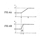
- a tuning voltage V T being outputted from the low-pass filter 10 is rising for a short pulse-width(PU), as shown in Fig. 4B, and from this, it can be noted that it is adjusted very fast compared to the case that the tuning voltage V T is increased gradually by the error signal Eo, as shown in Fig. 4A.
- the tuning voltage V T is adjusted by the error signal Eo in response to the phase difference between the reference frequency which has been set at the phase-locked loop and the voltage-controlled oscillation signal VCO being outputted from the tuner 1 so that the tuning state of the tuner 1 is maintained.
- the frequency(CF) of the presently receiving broadcasting signal is greater than the alterative frequency(AF) recorded in the designated address(AFA) of the alterative frequency list RAM
- the time is counted by the timer and the falling control pulse signal E1 is outputted in high level so as to be active.
- the alterative frequency(AF) is set as a reference frequency of the phase-locked loop.
- the falling control pulse signal E1 is outputted in low level so as to be unactive.
- the tuning voltage V T being outputted from the lopass filter 10 falls down for a short pulse-width(PU) to a tuning voltage inaccordance with the alterative frequency, and thereafter the tuning voltage V T is adjusted by an error signal Eo in response to the phase difference between the reference frequency which has been set at the phase-locked loop and the voltage-controlled oscillation signal VCO being outputted from the tuner 1 so that the tuning state of the tuner 1 is maintained.
- the counted time(TM) of the timer is greater than the delay time(TD) required in the practical tuning after the rising and falling control pulse signals E2 and E1 are unactive, that is, when the counted time(TM) of the timer is greater than the value of pulse-width(PU) + delay time(TD) after outputting the rising control pulse signal E2 or the falling control pulse signal E1, the address(AFL) of the RAM which stores the intermediate frequency level meter signal(ILM), is increased by "1" and the intermediate frequency level meter signal(ILM) being outputted from the intermediate frequency amplifying and detecting section 2 is inputted.
- the intermediate frequency level meter signal(ILM) is greater than a predetermined limiting level(SDL)
- the intermediate frequency level meter signal(ILM) is tored in the designated address(AFL) of the RAM. While, in case that the intermediate frequency level meter signal(ILM) is smaller than the predetermined limiting level(SDL), it is compared as to whether the designated address(AFA) of the alterative frequency list RAM is greater than the highest address(AFN) of the alterative frequency list RAM, and in case that it is smaller than the highest address(AFN), returning to the step of increasing the address(AFA) of the alterative frequency list RAM by "1" and then executing the next procedures repeatedly.
- the address(AFL) of the level meter signal storage RAM is designated to "1"
- the intermediate frequency level meter signal(ILM) stored in the designated address(AFL) is stored in a highest value storage RAM(MAXL) as a highest value.
- the intermediate frequency level meter signal(ILM) is stored again in the highest value storage RAM(MAXL) as a highest value, and thereafter in case that the intermediate frequency level meter signal(ILM) is smaller than the highest value stored in the highest value storage RAM(MAXL), an alterative frequency in accordance with the highest value is sought and stored in an alterative frequency highest RAM(AFMAX).
- alterative frequency is sought by adding a differential frequency(DC) in accordance with the relationship between the alterative frequency(AF) and the intermediate frequency level meter signal(ILM) to the highest value which has been read by the highest value storage RAM(MAXL), and then stored in the alterative frequency highest RAM(AFMAX). Thereafter, in case that the designated address(AFL) of the level meter signal storage RAM is smaller than the highest address(AFLN) of the level meter signal storage RAM, returning to the step of increasing the address(AFL) of the level meter signal storage RAM by "1" and executing the next procedures repeatedly.
- the alterative frequency stored in the alterative frequency highest RAM(AFMAX) is read out and then set as a reference frequency of the phase-locked loop.
- the present invention provides the effect that since when a field strength of the presently receiving broadcasting signal is kept maintained in a level below a predetermined level over a predetermined time, an alterative frequency is consecutively searched for on the alterative frequency list, rising or falling control pulse signal is outputted so as to reach a tuning voltage in accordance with the alterative frequency and the alterative frequency is set to a reference frequency of a phase-locked loop, it is possible to tune with the alterative frequency more quickly. Furthermore, since the highest alterative frequency whose the field strength of the receiving broadcasting signal is highest is searched for and tuned thereto, it is possible to provide the listers with convenience and reliability.
Landscapes
- Engineering & Computer Science (AREA)
- Signal Processing (AREA)
- Computer Hardware Design (AREA)
- Microelectronics & Electronic Packaging (AREA)
- Computer Networks & Wireless Communication (AREA)
- Circuits Of Receivers In General (AREA)
- Channel Selection Circuits, Automatic Tuning Circuits (AREA)
Applications Claiming Priority (2)
| Application Number | Priority Date | Filing Date | Title |
|---|---|---|---|
| KR1019900017649A KR0162294B1 (ko) | 1990-10-31 | 1990-10-31 | 알디에스의 대체주파수 고속서치 방법 및 장치 |
| KR1764990 | 1990-10-31 |
Publications (2)
| Publication Number | Publication Date |
|---|---|
| EP0484246A1 true EP0484246A1 (de) | 1992-05-06 |
| EP0484246B1 EP0484246B1 (de) | 1997-12-10 |
Family
ID=19305533
Family Applications (1)
| Application Number | Title | Priority Date | Filing Date |
|---|---|---|---|
| EP91402928A Expired - Lifetime EP0484246B1 (de) | 1990-10-31 | 1991-10-31 | Hochgeschwindigkeitsverfahren zur Suche einer alternativen Frequenz in einem Radiosystem |
Country Status (3)
| Country | Link |
|---|---|
| EP (1) | EP0484246B1 (de) |
| KR (1) | KR0162294B1 (de) |
| DE (1) | DE69128412T2 (de) |
Cited By (5)
| Publication number | Priority date | Publication date | Assignee | Title |
|---|---|---|---|---|
| US5572201A (en) * | 1994-08-05 | 1996-11-05 | Federal Signal Corporation | Alerting device and system for abnormal situations |
| WO1997023957A1 (de) * | 1995-12-23 | 1997-07-03 | Robert Bosch Gmbh | Mischoszillator mit einem phasengerasteten regelkreis für einen rundfunkempfänger |
| FR2753021A1 (fr) * | 1996-08-30 | 1998-03-06 | Sgs Thomson Microelectronics | Procede de selection de frequence dans un recepteur rds |
| WO2006131788A1 (en) * | 2005-06-07 | 2006-12-14 | Nokia Corporation | Receiving devices |
| EP1748558A1 (de) * | 2005-07-27 | 2007-01-31 | Robert Bosch Gmbh | Rundfunkempfangseinheit |
Families Citing this family (1)
| Publication number | Priority date | Publication date | Assignee | Title |
|---|---|---|---|---|
| DE19510220A1 (de) * | 1995-03-21 | 1996-09-26 | Blaupunkt Werke Gmbh | Rundfunkempfänger |
Citations (3)
| Publication number | Priority date | Publication date | Assignee | Title |
|---|---|---|---|---|
| DE3149409A1 (de) * | 1980-12-16 | 1982-09-16 | Mitsubishi Denki K.K., Tokyo | Rundfunkempfaenger |
| EP0275527A1 (de) * | 1986-12-19 | 1988-07-27 | TELEFUNKEN Fernseh und Rundfunk GmbH | Verfahren zum Übertragen und/oder zum empfangsseitigen Auswerten zusätzlicher Informationen innerhalb eines Rundfunksignals |
| GB2208457A (en) * | 1987-08-01 | 1989-03-30 | Pioneer Electronic Corp | Radio data system protocol discrimination |
-
1990
- 1990-10-31 KR KR1019900017649A patent/KR0162294B1/ko not_active Expired - Fee Related
-
1991
- 1991-10-31 DE DE69128412T patent/DE69128412T2/de not_active Expired - Lifetime
- 1991-10-31 EP EP91402928A patent/EP0484246B1/de not_active Expired - Lifetime
Patent Citations (3)
| Publication number | Priority date | Publication date | Assignee | Title |
|---|---|---|---|---|
| DE3149409A1 (de) * | 1980-12-16 | 1982-09-16 | Mitsubishi Denki K.K., Tokyo | Rundfunkempfaenger |
| EP0275527A1 (de) * | 1986-12-19 | 1988-07-27 | TELEFUNKEN Fernseh und Rundfunk GmbH | Verfahren zum Übertragen und/oder zum empfangsseitigen Auswerten zusätzlicher Informationen innerhalb eines Rundfunksignals |
| GB2208457A (en) * | 1987-08-01 | 1989-03-30 | Pioneer Electronic Corp | Radio data system protocol discrimination |
Cited By (7)
| Publication number | Priority date | Publication date | Assignee | Title |
|---|---|---|---|---|
| US5572201A (en) * | 1994-08-05 | 1996-11-05 | Federal Signal Corporation | Alerting device and system for abnormal situations |
| WO1997023957A1 (de) * | 1995-12-23 | 1997-07-03 | Robert Bosch Gmbh | Mischoszillator mit einem phasengerasteten regelkreis für einen rundfunkempfänger |
| FR2753021A1 (fr) * | 1996-08-30 | 1998-03-06 | Sgs Thomson Microelectronics | Procede de selection de frequence dans un recepteur rds |
| EP0837574A1 (de) * | 1996-08-30 | 1998-04-22 | STMicroelectronics S.A. | Verfahren für die Suche eines Kanals in einem RDS Empfänger |
| WO2006131788A1 (en) * | 2005-06-07 | 2006-12-14 | Nokia Corporation | Receiving devices |
| US7970369B2 (en) | 2005-06-07 | 2011-06-28 | Nokia Corporation | Receiving devices |
| EP1748558A1 (de) * | 2005-07-27 | 2007-01-31 | Robert Bosch Gmbh | Rundfunkempfangseinheit |
Also Published As
| Publication number | Publication date |
|---|---|
| EP0484246B1 (de) | 1997-12-10 |
| DE69128412D1 (de) | 1998-01-22 |
| KR920009103A (ko) | 1992-05-28 |
| KR0162294B1 (ko) | 1998-12-01 |
| DE69128412T2 (de) | 1998-06-04 |
Similar Documents
| Publication | Publication Date | Title |
|---|---|---|
| JP3187108B2 (ja) | ラジオ受信機 | |
| US5349699A (en) | Radio receiver with masking of switchover noise | |
| US4405947A (en) | Dual search mode type tuning system | |
| US5739762A (en) | Time correction system for radio selective calling receiver | |
| US5535442A (en) | FM tuner having improved tuning speed | |
| EP0484246B1 (de) | Hochgeschwindigkeitsverfahren zur Suche einer alternativen Frequenz in einem Radiosystem | |
| JP2571247B2 (ja) | ラジオデータ受信機における受信周波数選択方法 | |
| US4819069A (en) | Television signal selection device | |
| US4989263A (en) | Radio receiver with automatic mode changeover circuit | |
| JP2627284B2 (ja) | Rds受信機 | |
| JPS643383B2 (de) | ||
| EP0508369A1 (de) | Verfahren zum Wählen eines Senders für einen RDS-Empfänger | |
| EP0552442B1 (de) | Empfänger für ein Radio-Daten-System | |
| JPH0529164B2 (de) | ||
| US6452919B1 (en) | Assessment of digital signals, especially radio data signals | |
| JP2567634B2 (ja) | Rds受信機 | |
| KR100192451B1 (ko) | 디지탈 오디오 방송 수신기에서의 전송모드 판별방법 및 장치 | |
| JP3135763B2 (ja) | 多重放送受信機 | |
| KR100194992B1 (ko) | Fm 다중 방송 수신 장치 | |
| JP3354417B2 (ja) | Rds受信機のオートプリセット方法 | |
| KR100314963B1 (ko) | 방송수신기의방송수신방법 | |
| JPS60143029A (ja) | ラジオ受信機 | |
| JPH0738597B2 (ja) | 自動追従方法 | |
| JP3831483B2 (ja) | Fm多重放送の受信装置 | |
| JPH0758790A (ja) | クロック再生回路 |
Legal Events
| Date | Code | Title | Description |
|---|---|---|---|
| PUAI | Public reference made under article 153(3) epc to a published international application that has entered the european phase |
Free format text: ORIGINAL CODE: 0009012 |
|
| AK | Designated contracting states |
Kind code of ref document: A1 Designated state(s): DE FR GB IT |
|
| 17P | Request for examination filed |
Effective date: 19921024 |
|
| 17Q | First examination report despatched |
Effective date: 19941019 |
|
| RAP1 | Party data changed (applicant data changed or rights of an application transferred) |
Owner name: LG ELECTRONICS INC. |
|
| GRAG | Despatch of communication of intention to grant |
Free format text: ORIGINAL CODE: EPIDOS AGRA |
|
| GRAG | Despatch of communication of intention to grant |
Free format text: ORIGINAL CODE: EPIDOS AGRA |
|
| GRAH | Despatch of communication of intention to grant a patent |
Free format text: ORIGINAL CODE: EPIDOS IGRA |
|
| GRAH | Despatch of communication of intention to grant a patent |
Free format text: ORIGINAL CODE: EPIDOS IGRA |
|
| GRAH | Despatch of communication of intention to grant a patent |
Free format text: ORIGINAL CODE: EPIDOS IGRA |
|
| GRAA | (expected) grant |
Free format text: ORIGINAL CODE: 0009210 |
|
| ITF | It: translation for a ep patent filed | ||
| AK | Designated contracting states |
Kind code of ref document: B1 Designated state(s): DE FR GB IT |
|
| REF | Corresponds to: |
Ref document number: 69128412 Country of ref document: DE Date of ref document: 19980122 |
|
| ET | Fr: translation filed | ||
| PLBE | No opposition filed within time limit |
Free format text: ORIGINAL CODE: 0009261 |
|
| STAA | Information on the status of an ep patent application or granted ep patent |
Free format text: STATUS: NO OPPOSITION FILED WITHIN TIME LIMIT |
|
| 26N | No opposition filed | ||
| REG | Reference to a national code |
Ref country code: GB Ref legal event code: IF02 |
|
| PGFP | Annual fee paid to national office [announced via postgrant information from national office to epo] |
Ref country code: DE Payment date: 20091029 Year of fee payment: 19 |
|
| PGFP | Annual fee paid to national office [announced via postgrant information from national office to epo] |
Ref country code: IT Payment date: 20091022 Year of fee payment: 19 Ref country code: FR Payment date: 20091029 Year of fee payment: 19 Ref country code: GB Payment date: 20091028 Year of fee payment: 19 |
|
| GBPC | Gb: european patent ceased through non-payment of renewal fee |
Effective date: 20101031 |
|
| PG25 | Lapsed in a contracting state [announced via postgrant information from national office to epo] |
Ref country code: FR Free format text: LAPSE BECAUSE OF NON-PAYMENT OF DUE FEES Effective date: 20101102 |
|
| REG | Reference to a national code |
Ref country code: FR Ref legal event code: ST Effective date: 20110630 |
|
| REG | Reference to a national code |
Ref country code: DE Ref legal event code: R119 Ref document number: 69128412 Country of ref document: DE Effective date: 20110502 |
|
| PG25 | Lapsed in a contracting state [announced via postgrant information from national office to epo] |
Ref country code: GB Free format text: LAPSE BECAUSE OF NON-PAYMENT OF DUE FEES Effective date: 20101031 |
|
| PG25 | Lapsed in a contracting state [announced via postgrant information from national office to epo] |
Ref country code: IT Free format text: LAPSE BECAUSE OF NON-PAYMENT OF DUE FEES Effective date: 20101031 |
|
| PG25 | Lapsed in a contracting state [announced via postgrant information from national office to epo] |
Ref country code: DE Free format text: LAPSE BECAUSE OF NON-PAYMENT OF DUE FEES Effective date: 20110502 |