EP0484808A2 - Procédé et dispositif de métallisation sélective - Google Patents
Procédé et dispositif de métallisation sélective Download PDFInfo
- Publication number
- EP0484808A2 EP0484808A2 EP91118471A EP91118471A EP0484808A2 EP 0484808 A2 EP0484808 A2 EP 0484808A2 EP 91118471 A EP91118471 A EP 91118471A EP 91118471 A EP91118471 A EP 91118471A EP 0484808 A2 EP0484808 A2 EP 0484808A2
- Authority
- EP
- European Patent Office
- Prior art keywords
- substrate
- metal
- metallic layers
- solution
- organometallic compound
- Prior art date
- Legal status (The legal status is an assumption and is not a legal conclusion. Google has not performed a legal analysis and makes no representation as to the accuracy of the status listed.)
- Withdrawn
Links
Images
Classifications
-
- H—ELECTRICITY
- H05—ELECTRIC TECHNIQUES NOT OTHERWISE PROVIDED FOR
- H05K—PRINTED CIRCUITS; CASINGS OR CONSTRUCTIONAL DETAILS OF ELECTRIC APPARATUS; MANUFACTURE OF ASSEMBLAGES OF ELECTRICAL COMPONENTS
- H05K3/00—Apparatus or processes for manufacturing printed circuits
- H05K3/10—Apparatus or processes for manufacturing printed circuits in which conductive material is applied to the insulating support in such a manner as to form the desired conductive pattern
- H05K3/105—Apparatus or processes for manufacturing printed circuits in which conductive material is applied to the insulating support in such a manner as to form the desired conductive pattern by conversion of non-conductive material on or in the support into conductive material, e.g. by using an energy beam
-
- C—CHEMISTRY; METALLURGY
- C23—COATING METALLIC MATERIAL; COATING MATERIAL WITH METALLIC MATERIAL; CHEMICAL SURFACE TREATMENT; DIFFUSION TREATMENT OF METALLIC MATERIAL; COATING BY VACUUM EVAPORATION, BY SPUTTERING, BY ION IMPLANTATION OR BY CHEMICAL VAPOUR DEPOSITION, IN GENERAL; INHIBITING CORROSION OF METALLIC MATERIAL OR INCRUSTATION IN GENERAL
- C23C—COATING METALLIC MATERIAL; COATING MATERIAL WITH METALLIC MATERIAL; SURFACE TREATMENT OF METALLIC MATERIAL BY DIFFUSION INTO THE SURFACE, BY CHEMICAL CONVERSION OR SUBSTITUTION; COATING BY VACUUM EVAPORATION, BY SPUTTERING, BY ION IMPLANTATION OR BY CHEMICAL VAPOUR DEPOSITION, IN GENERAL
- C23C18/00—Chemical coating by decomposition of either liquid compounds or solutions of the coating forming compounds, without leaving reaction products of surface material in the coating; Contact plating
- C23C18/14—Decomposition by irradiation, e.g. photolysis, particle radiation or by mixed irradiation sources
- C23C18/143—Radiation by light, e.g. photolysis or pyrolysis
-
- H—ELECTRICITY
- H05—ELECTRIC TECHNIQUES NOT OTHERWISE PROVIDED FOR
- H05K—PRINTED CIRCUITS; CASINGS OR CONSTRUCTIONAL DETAILS OF ELECTRIC APPARATUS; MANUFACTURE OF ASSEMBLAGES OF ELECTRICAL COMPONENTS
- H05K3/00—Apparatus or processes for manufacturing printed circuits
- H05K3/10—Apparatus or processes for manufacturing printed circuits in which conductive material is applied to the insulating support in such a manner as to form the desired conductive pattern
- H05K3/12—Apparatus or processes for manufacturing printed circuits in which conductive material is applied to the insulating support in such a manner as to form the desired conductive pattern using thick film techniques, e.g. printing techniques to apply the conductive material or similar techniques for applying conductive paste or ink patterns
- H05K3/1241—Apparatus or processes for manufacturing printed circuits in which conductive material is applied to the insulating support in such a manner as to form the desired conductive pattern using thick film techniques, e.g. printing techniques to apply the conductive material or similar techniques for applying conductive paste or ink patterns by ink-jet printing or drawing by dispensing
- H05K3/125—Apparatus or processes for manufacturing printed circuits in which conductive material is applied to the insulating support in such a manner as to form the desired conductive pattern using thick film techniques, e.g. printing techniques to apply the conductive material or similar techniques for applying conductive paste or ink patterns by ink-jet printing or drawing by dispensing by ink-jet printing
-
- H—ELECTRICITY
- H05—ELECTRIC TECHNIQUES NOT OTHERWISE PROVIDED FOR
- H05K—PRINTED CIRCUITS; CASINGS OR CONSTRUCTIONAL DETAILS OF ELECTRIC APPARATUS; MANUFACTURE OF ASSEMBLAGES OF ELECTRICAL COMPONENTS
- H05K2201/00—Indexing scheme relating to printed circuits covered by H05K1/00
- H05K2201/03—Conductive materials
- H05K2201/0332—Structure of the conductor
- H05K2201/0335—Layered conductors or foils
- H05K2201/0347—Overplating, e.g. for reinforcing conductors or bumps; Plating over filled vias
-
- H—ELECTRICITY
- H05—ELECTRIC TECHNIQUES NOT OTHERWISE PROVIDED FOR
- H05K—PRINTED CIRCUITS; CASINGS OR CONSTRUCTIONAL DETAILS OF ELECTRIC APPARATUS; MANUFACTURE OF ASSEMBLAGES OF ELECTRICAL COMPONENTS
- H05K2203/00—Indexing scheme relating to apparatus or processes for manufacturing printed circuits covered by H05K3/00
- H05K2203/01—Tools for processing; Objects used during processing
- H05K2203/0104—Tools for processing; Objects used during processing for patterning or coating
- H05K2203/013—Inkjet printing, e.g. for printing insulating material or resist
-
- H—ELECTRICITY
- H05—ELECTRIC TECHNIQUES NOT OTHERWISE PROVIDED FOR
- H05K—PRINTED CIRCUITS; CASINGS OR CONSTRUCTIONAL DETAILS OF ELECTRIC APPARATUS; MANUFACTURE OF ASSEMBLAGES OF ELECTRICAL COMPONENTS
- H05K2203/00—Indexing scheme relating to apparatus or processes for manufacturing printed circuits covered by H05K3/00
- H05K2203/12—Using specific substances
- H05K2203/121—Metallo-organic compounds
Definitions
- the invention relates to a method and a device for producing partial metallic layers from a metal-containing, in particular organometallic compound on a substrate by irradiation with a light source.
- the invention is based on the object of specifying a method and a device for producing partial metallic layers with which structured metallizations can be applied to any substrate in a simple, environmentally friendly and economical manner.
- This object is achieved with respect to the method in that the metal-containing, in particular organometallic compound is applied to the surface of the substrate using a writing device in the form of a solution film which contains the metal-containing, in particular organometallic compound, and in that the metal-containing, in particular organometallic compound is then exposed to the action of UV photons of a defined wavelength.
- the object is achieved with respect to the device by means of a writing device which can be supplied with a solution containing a metal-containing, in particular organometallic compound on the input side and applies this solution to the substrate via a nozzle on the output side, the writing device and substrate being arbitrary in the XYZ direction against one another at high speeds are movable.
- Quartz, glass and silicon, light flexible plastics (Teflon, polyimides etc.) rubber, plastic or glass fleece, ceramic filled or glass fiber reinforced fluoroplastics, press boards and paper or cardboard with low temperature resistance can be produced. All substrate materials can be coated with the same good quality.
- the layers have good adhesive strength and electrical conductivity and are easily solderable and bondable.
- fine structure technology encompasses the creation of the finest conductor tracks and structures with very close spacings, as a result of which a high integration density is achieved. This allows components, e.g. Coils, solar cells, display cells etc., can be miniaturized. Such components with increased packing density are of interest for microelectronics in general, printed circuit board technology, hybrid and sensor technology and for decorative applications.
- the proposed method is relatively little time-consuming and very economical.
- the proposed device is user-friendly, inexpensive and fast in the production of fine structure technology on any substrate surface.
- the proposed method allows considerable savings to be made in the methods used. partly achieve expensive organometallic substances, since from the start only the areas to be metallized are wetted with the solvent film.
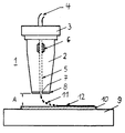
- a writing device 1 can be seen with a housing 2 with cover 3 and bottom 8, a pipe connection 4 in the cover 3 for the solution supply, a capillary 5 which extends from the pipe connection 4 to the nozzle 7 in the bottom 8 and with a piezoelectric transducer (transducer) 6, which encloses the capillary 5 and is used to express the solution from the nozzle 7.
- Impulse jets, thermal jets or aerosol jets can be used, with jet being a liquid jet.
- a fiber pen, a ballpoint pen, a fountain pen or an ink pen can also be used as writing instruments.
- the liquid drops 11 squeezed out of the nozzle 7 wet the substrate 10 arranged below the nozzle 7 of the writing device, as a result of which a "written" Structure 12 is formed on the substrate 10.
- the distance A between nozzle 7 and substrate 10 is preferably 1 mm.
- the substrate 10 is preferably fastened on a computer-controlled XYZ shift table 9, so that any desired structuring of the substrate 10 with solution is possible by shifting the table 9 in the X or Y or Z or in the X and Y and Z directions is.
- Simultaneous displacement of both the writing device 1 and the displacement table 9 with substrate 10 is also possible, as a result of which the structuring speed is further increased.
- a writing process with liquid, organometallic or other metal-containing compounds is therefore used in combination with the computer technology in order to write any structures such as conductor tracks, connections, coils, meanders etc. on any surfaces (line width, for example 50 ⁇ m ).
- Calculated metal patterns can be generated directly with computer-controlled writing devices.
- a scanning device line scanner
- Another advantage of computer technology in connection with the technology described is that the writing device over Data lines can be controlled remotely, and that several such writing devices can be controlled by a (possibly distant) computer.
- a central writing device can be operated by different computers.
- Organometallic and other metal-containing compounds are used as compounds, such as palladium acetate, palladium acetylacetonate, palladium chloride, cobalt acetate, nickel acetate, copper formate, silver neodecanates, cyclopentadienyl palladium allyl or cyclopentadienyl palladium chloride etc., which have strong absorption bands in the UV range from 60 nm to 400 nm.
- solvents e.g. Chloroform, alcohol, water and others used.
- the solution can be chloroform containing palladium acetate. It is also possible to dissolve cyclopentadienylpalladium allyl, which is in powder form, in alcohol or water and to apply it to the substrate. The use of powdered cyclopentadienyl palladium chloride, which is also dissolved in alcohol or water to form a solution, is also possible.
- the solutions are preferably applied to the substrate so thick that the metallic layer has a thickness between 0.5 and 50 nm.
- UV radiation is used in order to achieve the decomposition of the non-conductive organometallic compounds by exposing the thin organometallic layer structures and to effect a deposition of the corresponding metals (UV-assisted deposition of a catalyst from organometallic adsorbates on the substrate surface. Because this is ultraviolet The substrate material remains unaffected. The properties of the substrate material play only an insignificant role in the deposition process.
- An incoherent excimer light source with the desired wavelength is preferably used as the UV source. A detailed description of such a high-power radiator can be found in EP-OS 0 254 111.
- the high-performance radiator consists of a metal electrode cooled by a metal electrode and a dielectric or two dielectrics delimited and filled with a noble gas or gas mixture discharge space.
- the dielectric and the second electrode lying on the surface of the dielectric facing away from the discharge space are transparent to the radiation generated by the silent electrical discharge.
- a wavelength of 300 to 320 nm can be generated with the high-power radiator.
- the high-performance radiator works in quasi-pulsed operation. If the entire surface of the substrate to be coated is to be provided with a metal structure, a high-power radiator is used, the radiation field of which corresponds to the size of the substrate surface. The irradiation can be carried out for a few seconds up to a few minutes, depending on the circumstances, application thickness and distance between the substrate surface and the UV high-power lamp.
- a high-power mercury lamp can also be used for the formation of the metallic layers.
- the geometry of the UV high-power lamp or high-performance mercury lamp used can be adapted to the geometry of the substrates to be coated. It is quite possible, for example, that Carry out coating of rectangular substrates on a conveyor belt every second. For this purpose, the lamp geometry is matched to the rectangular cross section of the substrate to be coated.
- the length of the lamp and the speed of the belt on which the substrates are placed are coordinated with one another such that the respective substrate is moved under a lamp for as long as is necessary for the formation of the metallic layer on its surface.
- the desired production rate can be achieved by choosing the above parameters.
- electroless chemical processes or direct galvanic processes are used to effect the actual layer structure.
- a large number of metals such as Cu, Ni, Pd, Pt, Al, Au, Cr, Sn etc. can be deposited in a structured manner, whereby a layer thickness of up to a few 100 ⁇ m can be achieved.
- the activated areas are electrolessly metallized in commercially available bathrooms. Typical bath temperatures are between room temperature and 100 ° C.
- chemical metallization processes in addition to the high layer thicknesses to be achieved, have the significant advantage that the metallization of complicatedly shaped workpieces with a homogeneous layer thickness distribution is possible. With the help of this technology, it is therefore also possible to metallize curved surfaces.
- the chemical metallization processes that are widely used, only the pretreatment and Activation of the surfaces requires approx. 12 wet chemical baths before the actual metallization bath is used (eg Shipley process). Further process steps (coating with lacquer, exposure, etching of lacquer and metal layers, removal of lacquer residues) are then required for structuring the metal layers, so that a total of approximately 20 process steps are disadvantageously necessary for producing structured metal layers.
- An overall system suitable for series production for the production of partial metallic layers consists, for example, of a computer-controlled solution jet recorder, an incoherent excimer radiation source and a chemical metallization bath, and possibly an additional microscope with monitor.
- the structured substrates are manufactured in continuous operation with high throughput. Important applications can also be seen in circuit modifications: repair and adjustment of circuits.
Landscapes
- Chemical & Material Sciences (AREA)
- Engineering & Computer Science (AREA)
- Manufacturing & Machinery (AREA)
- Microelectronics & Electronic Packaging (AREA)
- General Chemical & Material Sciences (AREA)
- Toxicology (AREA)
- Health & Medical Sciences (AREA)
- Chemical Kinetics & Catalysis (AREA)
- Materials Engineering (AREA)
- Mechanical Engineering (AREA)
- Metallurgy (AREA)
- Organic Chemistry (AREA)
- Chemically Coating (AREA)
- Electroplating And Plating Baths Therefor (AREA)
- Manufacturing Of Printed Wiring (AREA)
Applications Claiming Priority (2)
| Application Number | Priority Date | Filing Date | Title |
|---|---|---|---|
| DE4035080 | 1990-11-05 | ||
| DE4035080A DE4035080A1 (de) | 1990-11-05 | 1990-11-05 | Verfahren und einrichtung zur herstellung von partiellen metallischen schichten |
Publications (2)
| Publication Number | Publication Date |
|---|---|
| EP0484808A2 true EP0484808A2 (fr) | 1992-05-13 |
| EP0484808A3 EP0484808A3 (fr) | 1994-02-09 |
Family
ID=6417641
Family Applications (1)
| Application Number | Title | Priority Date | Filing Date |
|---|---|---|---|
| EP91118471A Withdrawn EP0484808A2 (fr) | 1990-11-05 | 1991-10-30 | Procédé et dispositif de métallisation sélective |
Country Status (3)
| Country | Link |
|---|---|
| EP (1) | EP0484808A2 (fr) |
| JP (1) | JPH04272182A (fr) |
| DE (1) | DE4035080A1 (fr) |
Cited By (12)
| Publication number | Priority date | Publication date | Assignee | Title |
|---|---|---|---|---|
| EP0651073A1 (fr) * | 1993-10-29 | 1995-05-03 | General Electric Company | Solution d'acétylacétonate de palladium |
| WO1995031586A1 (fr) * | 1994-05-11 | 1995-11-23 | Kimberly-Clark Corporation | Procede d'enduction d'un substrat avec du cuivre |
| EP0696813A1 (fr) * | 1994-08-11 | 1996-02-14 | Canon Kabushiki Kaisha | Solution pour la fabrication des dispositifs émetteur d'électrons, méthode de fabrication des dispositifs émetteur d'électrons, et méthode de fabrication de dispositif de formation d'images |
| EP0588038B1 (fr) * | 1992-09-09 | 1996-09-18 | Heraeus Noblelight GmbH | Procédé de dépÔt d'une couche d'oxyde protectrice |
| GB2376344A (en) * | 1997-10-14 | 2002-12-11 | Patterning Technologies Ltd | Method of forming an electronic device |
| WO2004017688A1 (fr) * | 2002-08-16 | 2004-02-26 | Qinetiq Limited | Depot de matieres solides |
| WO2005079126A3 (fr) * | 2004-02-10 | 2005-12-01 | Plastic Logic Ltd | Depot metallique |
| WO2006014265A1 (fr) | 2004-07-06 | 2006-02-09 | Hewlett-Packard Development Company, L.P. | Formation d'une structure |
| US7129166B2 (en) | 1997-10-14 | 2006-10-31 | Patterning Technologies Limited | Method of forming an electronic device |
| US7323634B2 (en) | 1998-10-14 | 2008-01-29 | Patterning Technologies Limited | Method of forming an electronic device |
| CN100522643C (zh) * | 2004-06-15 | 2009-08-05 | 惠普发展公司 | 印刷有机金属化合物以形成导电迹线 |
| WO2022161616A1 (fr) * | 2021-01-29 | 2022-08-04 | Midnex Ag | Procédé et dispositif d'application d'un revêtement métallique sur une surface |
Families Citing this family (7)
| Publication number | Priority date | Publication date | Assignee | Title |
|---|---|---|---|---|
| JP4503792B2 (ja) * | 1999-08-11 | 2010-07-14 | 三ツ星ベルト株式会社 | セラミックス回路基板の製造方法 |
| DE20204442U1 (de) | 2002-03-15 | 2002-06-20 | Wieland Dental + Technik GmbH & Co. KG, 75179 Pforzheim | Leitfähigkeitsstift |
| JP2006075744A (ja) * | 2004-09-10 | 2006-03-23 | Jsr Corp | アルミニウムパターンの形成方法 |
| DE102006030822A1 (de) * | 2006-06-30 | 2008-01-03 | Fraunhofer-Gesellschaft zur Förderung der angewandten Forschung e.V. | Verfahren zum Herstellen einer metallischen Kontaktstruktur einer Solarzelle |
| DE102007058972A1 (de) | 2007-12-07 | 2009-07-09 | Fraunhofer-Gesellschaft zur Förderung der angewandten Forschung e.V. | Verfahren zur Metallisierung von Solarzellen, Hotmelt-Aerosol-Tinte und Aerosol-Jet-Drucksystem |
| JP5382797B2 (ja) * | 2009-09-30 | 2014-01-08 | 独立行政法人産業技術総合研究所 | 導電性組成物を用いた電気化学反応による構造体の作製方法 |
| JP5382796B2 (ja) * | 2009-09-30 | 2014-01-08 | 独立行政法人産業技術総合研究所 | 導電性組成物および電気化学反応方法および構造体 |
Family Cites Families (13)
| Publication number | Priority date | Publication date | Assignee | Title |
|---|---|---|---|---|
| DE2757029A1 (de) * | 1977-12-21 | 1980-01-31 | Guenther Dr Ing Herrmann | Verfahren zur herstellung einer schaltungsplatte |
| JPS56164595A (en) * | 1980-05-23 | 1981-12-17 | Tokyo Shibaura Electric Co | Method of producing circuit board |
| DE3047884A1 (de) * | 1980-12-18 | 1982-07-15 | Siemens AG, 1000 Berlin und 8000 München | Vorrichtung zur automatisierbaren bearbeitung in der halbleitertechnologie, z.b. von leiterplatten |
| JPS59112685A (ja) * | 1982-12-17 | 1984-06-29 | 松下電器産業株式会社 | 電子回路板の製造方法 |
| JPS59177358A (ja) * | 1983-03-28 | 1984-10-08 | Nec Corp | 局所金属堆積方法および装置 |
| DE3326508A1 (de) * | 1983-07-22 | 1985-02-07 | Bayer Ag, 5090 Leverkusen | Verfahren zum aktivieren von substratoberflaechen fuer die direkte partielle metallisierung von traegermaterialien |
| WO1986001067A1 (fr) * | 1984-07-26 | 1986-02-13 | Matsushita Electric Industrial Co., Ltd. | Procede et dispositif de production de circuits a film epais |
| US4668533A (en) * | 1985-05-10 | 1987-05-26 | E. I. Du Pont De Nemours And Company | Ink jet printing of printed circuit boards |
| JPS63192874A (ja) * | 1987-02-06 | 1988-08-10 | Electroplating Eng Of Japan Co | 金属被膜品の製造方法 |
| NL8700833A (nl) * | 1987-04-09 | 1988-11-01 | Philips Nv | Werkwijze voor het vervaardigen van een gedrukte bedradingspaneel. |
| JPH01196194A (ja) * | 1988-02-01 | 1989-08-07 | Matsushita Electric Ind Co Ltd | 回路描画装置 |
| DE58907207D1 (de) * | 1988-07-02 | 1994-04-21 | Heraeus Noblelight Gmbh | Verfahren zur Herstellung von metallischen Schichten. |
| DE3840199C2 (de) * | 1988-11-29 | 1994-12-01 | Heraeus Noblelight Gmbh | Verfahren zur Strukturierung von bei der stromlosen Metallisierung katalytisch aktiven Metallschichten mittels UV-Strahlung |
-
1990
- 1990-11-05 DE DE4035080A patent/DE4035080A1/de not_active Ceased
-
1991
- 1991-10-30 EP EP91118471A patent/EP0484808A2/fr not_active Withdrawn
- 1991-10-31 JP JP3286785A patent/JPH04272182A/ja active Pending
Cited By (19)
| Publication number | Priority date | Publication date | Assignee | Title |
|---|---|---|---|---|
| EP0588038B1 (fr) * | 1992-09-09 | 1996-09-18 | Heraeus Noblelight GmbH | Procédé de dépÔt d'une couche d'oxyde protectrice |
| EP0651073A1 (fr) * | 1993-10-29 | 1995-05-03 | General Electric Company | Solution d'acétylacétonate de palladium |
| US5448605A (en) * | 1993-10-29 | 1995-09-05 | General Electric Company | Palladium acetylacetonate solution and related method of manufacture |
| WO1995031586A1 (fr) * | 1994-05-11 | 1995-11-23 | Kimberly-Clark Corporation | Procede d'enduction d'un substrat avec du cuivre |
| EP0696813A1 (fr) * | 1994-08-11 | 1996-02-14 | Canon Kabushiki Kaisha | Solution pour la fabrication des dispositifs émetteur d'électrons, méthode de fabrication des dispositifs émetteur d'électrons, et méthode de fabrication de dispositif de formation d'images |
| US5716618A (en) * | 1994-08-11 | 1998-02-10 | Canon Kabushiki Kaisha | Solution for fabrication of electron-emitting devices, manufacture method of electron-emitting devices, and manufacture method of image-forming apparatus |
| USRE37896E1 (en) * | 1994-08-11 | 2002-10-29 | Canon Kabushiki Kaisha | Solution for fabrication of electron-emitting devices, manufacture method of electron-emitting devices, and manufacture method of image-forming apparatus |
| GB2376344B (en) * | 1997-10-14 | 2003-02-19 | Patterning Technologies Ltd | Method of forming an electronic device |
| GB2376344A (en) * | 1997-10-14 | 2002-12-11 | Patterning Technologies Ltd | Method of forming an electronic device |
| US7129166B2 (en) | 1997-10-14 | 2006-10-31 | Patterning Technologies Limited | Method of forming an electronic device |
| US7323634B2 (en) | 1998-10-14 | 2008-01-29 | Patterning Technologies Limited | Method of forming an electronic device |
| WO2004017688A1 (fr) * | 2002-08-16 | 2004-02-26 | Qinetiq Limited | Depot de matieres solides |
| WO2005079126A3 (fr) * | 2004-02-10 | 2005-12-01 | Plastic Logic Ltd | Depot metallique |
| US7867686B2 (en) | 2004-02-10 | 2011-01-11 | Plastic Logic Limited | Metal deposition |
| CN100522643C (zh) * | 2004-06-15 | 2009-08-05 | 惠普发展公司 | 印刷有机金属化合物以形成导电迹线 |
| WO2006014265A1 (fr) | 2004-07-06 | 2006-02-09 | Hewlett-Packard Development Company, L.P. | Formation d'une structure |
| US7547647B2 (en) | 2004-07-06 | 2009-06-16 | Hewlett-Packard Development Company, L.P. | Method of making a structure |
| US8143616B2 (en) | 2004-07-06 | 2012-03-27 | Oregon State University | Making a structure |
| WO2022161616A1 (fr) * | 2021-01-29 | 2022-08-04 | Midnex Ag | Procédé et dispositif d'application d'un revêtement métallique sur une surface |
Also Published As
| Publication number | Publication date |
|---|---|
| EP0484808A3 (fr) | 1994-02-09 |
| DE4035080A1 (de) | 1992-05-07 |
| JPH04272182A (ja) | 1992-09-28 |
Similar Documents
| Publication | Publication Date | Title |
|---|---|---|
| DE4035080A1 (de) | Verfahren und einrichtung zur herstellung von partiellen metallischen schichten | |
| EP0792388B1 (fr) | Procede de fabrication par depot direct de films a motifs contenant du metal | |
| DE69507926T2 (de) | Verfahren zur erzeugung eines kupferbildes auf einer aus elektrisch nichtleitendem material bestehenden platte mittels eines photolithographischen verfahrens | |
| EP0917597B1 (fr) | Procede de production de structures de pistes conductrices, en particulier de structures fines de pistes conductrices, disposees sur un materiau support non conducteur | |
| DE3826046A1 (de) | Verfahren zur herstellung von metallischen schichten | |
| EP0287843A1 (fr) | Procédé de fabrication de plaques de circuits imprimés | |
| DE4330961C1 (de) | Verfahren zur Herstellung von strukturierten Metallisierungen auf Oberflächen | |
| EP0321734A1 (fr) | Procédé de fabrication de structures métalliques fortement adhérentes sur des fluoropolymères et des matériaux thermoplastiques | |
| DE4034834C2 (de) | Verfahren zur Herstellung metallischer Schichten auf Substraten und Verwendung der Schichten | |
| DE112006003613T5 (de) | Verfahren und Vorrichtung für eine Leiterplatte unter Verwendung der lasergestützten Metallisierung und Strukturierung eines Substrats | |
| Zhang et al. | Investigations of photo-induced decomposition of palladium acetate for electroless copper plating | |
| DE69204564T2 (de) | Verfahren zur selektiven stromlosen Metallisierung eines Musters aus einem anderen Werkstoff als Glas auf einem Glasträger. | |
| DE19642922C2 (de) | Aktivierende katalytische Lösung zur stromlosen Metallisierung und Verfahren zur Vorbereitung eines Substrats zur stromlosen Metallisierung | |
| WO1991009984A1 (fr) | Procede d'enduction | |
| DD157989A3 (de) | Verfahren zur strukturierten chemisch-reduktiven metallabscheidung | |
| EP0143951A2 (fr) | Procédé de métallisation chimique | |
| EP0534576B1 (fr) | Procédé pour le dépôt de couches métalliques texturées sur substrats en verre | |
| EP0349882B1 (fr) | Procédé de fabrication de couches métalliques | |
| EP0493709A2 (fr) | Procédé pour déposer une couche d'or sur la totalité ou une partie d'une surface | |
| DE3840199C2 (de) | Verfahren zur Strukturierung von bei der stromlosen Metallisierung katalytisch aktiven Metallschichten mittels UV-Strahlung | |
| EP0136364B1 (fr) | Procédé et dispositif pour la déposition sélective et autoréglée de couches de métal et application de ce procédé | |
| DE19951721A1 (de) | Verfahren zur strukturierten Metallisierung der Oberfläche von Substraten | |
| DE3430290A1 (de) | Verfahren zur selektiven metallisierung | |
| EP0813618B1 (fr) | Procede de metallisation sans courant de substrats non electroconducteurs | |
| EP1138803A2 (fr) | Procédé de métallisation d'un isolateur et/ou d'un diélectrique |
Legal Events
| Date | Code | Title | Description |
|---|---|---|---|
| PUAI | Public reference made under article 153(3) epc to a published international application that has entered the european phase |
Free format text: ORIGINAL CODE: 0009012 |
|
| AK | Designated contracting states |
Kind code of ref document: A2 Designated state(s): CH DE FR GB LI NL |
|
| RAP1 | Party data changed (applicant data changed or rights of an application transferred) |
Owner name: HERAEUS NOBLELIGHT GMBH |
|
| PUAL | Search report despatched |
Free format text: ORIGINAL CODE: 0009013 |
|
| AK | Designated contracting states |
Kind code of ref document: A3 Designated state(s): CH DE FR GB LI NL |
|
| 17P | Request for examination filed |
Effective date: 19940307 |
|
| 17Q | First examination report despatched |
Effective date: 19940805 |
|
| STAA | Information on the status of an ep patent application or granted ep patent |
Free format text: STATUS: THE APPLICATION IS DEEMED TO BE WITHDRAWN |
|
| 18D | Application deemed to be withdrawn |
Effective date: 19941216 |