EP0485760A1 - Procédé d'attachement d'une pièce à écroulement contrôlé à basse température - Google Patents
Procédé d'attachement d'une pièce à écroulement contrôlé à basse température Download PDFInfo
- Publication number
- EP0485760A1 EP0485760A1 EP91117796A EP91117796A EP0485760A1 EP 0485760 A1 EP0485760 A1 EP 0485760A1 EP 91117796 A EP91117796 A EP 91117796A EP 91117796 A EP91117796 A EP 91117796A EP 0485760 A1 EP0485760 A1 EP 0485760A1
- Authority
- EP
- European Patent Office
- Prior art keywords
- solder
- chip
- card
- circuit card
- microelectronic circuit
- Prior art date
- Legal status (The legal status is an assumption and is not a legal conclusion. Google has not performed a legal analysis and makes no representation as to the accuracy of the status listed.)
- Withdrawn
Links
Images

Classifications
-
- B—PERFORMING OPERATIONS; TRANSPORTING
- B23—MACHINE TOOLS; METAL-WORKING NOT OTHERWISE PROVIDED FOR
- B23K—SOLDERING OR UNSOLDERING; WELDING; CLADDING OR PLATING BY SOLDERING OR WELDING; CUTTING BY APPLYING HEAT LOCALLY, e.g. FLAME CUTTING; WORKING BY LASER BEAM
- B23K1/00—Soldering, e.g. brazing, or unsoldering
- B23K1/0008—Soldering, e.g. brazing, or unsoldering specially adapted for particular articles or work
- B23K1/0016—Soldering of electronic components
-
- H—ELECTRICITY
- H05—ELECTRIC TECHNIQUES NOT OTHERWISE PROVIDED FOR
- H05K—PRINTED CIRCUITS; CASINGS OR CONSTRUCTIONAL DETAILS OF ELECTRIC APPARATUS; MANUFACTURE OF ASSEMBLAGES OF ELECTRICAL COMPONENTS
- H05K3/00—Apparatus or processes for manufacturing printed circuits
- H05K3/30—Assembling printed circuits with electric components, e.g. with resistors
- H05K3/32—Assembling printed circuits with electric components, e.g. with resistors electrically connecting electric components or wires to printed circuits
- H05K3/34—Assembling printed circuits with electric components, e.g. with resistors electrically connecting electric components or wires to printed circuits by soldering
- H05K3/341—Surface mounted components
- H05K3/3431—Leadless components
- H05K3/3436—Leadless components having an array of bottom contacts, e.g. pad grid array or ball grid array components
-
- H—ELECTRICITY
- H05—ELECTRIC TECHNIQUES NOT OTHERWISE PROVIDED FOR
- H05K—PRINTED CIRCUITS; CASINGS OR CONSTRUCTIONAL DETAILS OF ELECTRIC APPARATUS; MANUFACTURE OF ASSEMBLAGES OF ELECTRICAL COMPONENTS
- H05K2201/00—Indexing scheme relating to printed circuits covered by H05K1/00
- H05K2201/10—Details of components or other objects attached to or integrated in a printed circuit board
- H05K2201/10613—Details of electrical connections of non-printed components, e.g. special leads
- H05K2201/10954—Other details of electrical connections
- H05K2201/10992—Using different connection materials, e.g. different solders, for the same connection
-
- H—ELECTRICITY
- H05—ELECTRIC TECHNIQUES NOT OTHERWISE PROVIDED FOR
- H05K—PRINTED CIRCUITS; CASINGS OR CONSTRUCTIONAL DETAILS OF ELECTRIC APPARATUS; MANUFACTURE OF ASSEMBLAGES OF ELECTRICAL COMPONENTS
- H05K2203/00—Indexing scheme relating to apparatus or processes for manufacturing printed circuits covered by H05K3/00
- H05K2203/04—Soldering or other types of metallurgic bonding
- H05K2203/0415—Small preforms other than balls, e.g. discs, cylinders or pillars
-
- H—ELECTRICITY
- H05—ELECTRIC TECHNIQUES NOT OTHERWISE PROVIDED FOR
- H05K—PRINTED CIRCUITS; CASINGS OR CONSTRUCTIONAL DETAILS OF ELECTRIC APPARATUS; MANUFACTURE OF ASSEMBLAGES OF ELECTRICAL COMPONENTS
- H05K3/00—Apparatus or processes for manufacturing printed circuits
- H05K3/30—Assembling printed circuits with electric components, e.g. with resistors
- H05K3/32—Assembling printed circuits with electric components, e.g. with resistors electrically connecting electric components or wires to printed circuits
- H05K3/34—Assembling printed circuits with electric components, e.g. with resistors electrically connecting electric components or wires to printed circuits by soldering
- H05K3/341—Surface mounted components
- H05K3/3431—Leadless components
-
- H—ELECTRICITY
- H05—ELECTRIC TECHNIQUES NOT OTHERWISE PROVIDED FOR
- H05K—PRINTED CIRCUITS; CASINGS OR CONSTRUCTIONAL DETAILS OF ELECTRIC APPARATUS; MANUFACTURE OF ASSEMBLAGES OF ELECTRICAL COMPONENTS
- H05K3/00—Apparatus or processes for manufacturing printed circuits
- H05K3/30—Assembling printed circuits with electric components, e.g. with resistors
- H05K3/32—Assembling printed circuits with electric components, e.g. with resistors electrically connecting electric components or wires to printed circuits
- H05K3/34—Assembling printed circuits with electric components, e.g. with resistors electrically connecting electric components or wires to printed circuits by soldering
- H05K3/3465—Application of solder
-
- H—ELECTRICITY
- H10—SEMICONDUCTOR DEVICES; ELECTRIC SOLID-STATE DEVICES NOT OTHERWISE PROVIDED FOR
- H10W—GENERIC PACKAGES, INTERCONNECTIONS, CONNECTORS OR OTHER CONSTRUCTIONAL DETAILS OF DEVICES COVERED BY CLASS H10
- H10W72/00—Interconnections or connectors in packages
- H10W72/071—Connecting or disconnecting
- H10W72/072—Connecting or disconnecting of bump connectors
- H10W72/07231—Techniques
- H10W72/07236—Soldering or alloying
-
- H—ELECTRICITY
- H10—SEMICONDUCTOR DEVICES; ELECTRIC SOLID-STATE DEVICES NOT OTHERWISE PROVIDED FOR
- H10W—GENERIC PACKAGES, INTERCONNECTIONS, CONNECTORS OR OTHER CONSTRUCTIONAL DETAILS OF DEVICES COVERED BY CLASS H10
- H10W72/00—Interconnections or connectors in packages
- H10W72/20—Bump connectors, e.g. solder bumps or copper pillars; Dummy bumps; Thermal bumps
- H10W72/251—Materials
- H10W72/252—Materials comprising solid metals or solid metalloids, e.g. PbSn, Ag or Cu
-
- H—ELECTRICITY
- H10—SEMICONDUCTOR DEVICES; ELECTRIC SOLID-STATE DEVICES NOT OTHERWISE PROVIDED FOR
- H10W—GENERIC PACKAGES, INTERCONNECTIONS, CONNECTORS OR OTHER CONSTRUCTIONAL DETAILS OF DEVICES COVERED BY CLASS H10
- H10W90/00—Package configurations
- H10W90/701—Package configurations characterised by the relative positions of pads or connectors relative to package parts
- H10W90/721—Package configurations characterised by the relative positions of pads or connectors relative to package parts of bump connectors
- H10W90/724—Package configurations characterised by the relative positions of pads or connectors relative to package parts of bump connectors between a chip and a stacked insulating package substrate, interposer or RDL
-
- Y—GENERAL TAGGING OF NEW TECHNOLOGICAL DEVELOPMENTS; GENERAL TAGGING OF CROSS-SECTIONAL TECHNOLOGIES SPANNING OVER SEVERAL SECTIONS OF THE IPC; TECHNICAL SUBJECTS COVERED BY FORMER USPC CROSS-REFERENCE ART COLLECTIONS [XRACs] AND DIGESTS
- Y02—TECHNOLOGIES OR APPLICATIONS FOR MITIGATION OR ADAPTATION AGAINST CLIMATE CHANGE
- Y02P—CLIMATE CHANGE MITIGATION TECHNOLOGIES IN THE PRODUCTION OR PROCESSING OF GOODS
- Y02P70/00—Climate change mitigation technologies in the production process for final industrial or consumer products
- Y02P70/50—Manufacturing or production processes characterised by the final manufactured product
-
- Y—GENERAL TAGGING OF NEW TECHNOLOGICAL DEVELOPMENTS; GENERAL TAGGING OF CROSS-SECTIONAL TECHNOLOGIES SPANNING OVER SEVERAL SECTIONS OF THE IPC; TECHNICAL SUBJECTS COVERED BY FORMER USPC CROSS-REFERENCE ART COLLECTIONS [XRACs] AND DIGESTS
- Y10—TECHNICAL SUBJECTS COVERED BY FORMER USPC
- Y10T—TECHNICAL SUBJECTS COVERED BY FORMER US CLASSIFICATION
- Y10T29/00—Metal working
- Y10T29/49—Method of mechanical manufacture
- Y10T29/49002—Electrical device making
- Y10T29/49117—Conductor or circuit manufacturing
- Y10T29/49124—On flat or curved insulated base, e.g., printed circuit, etc.
- Y10T29/4913—Assembling to base an electrical component, e.g., capacitor, etc.
- Y10T29/49144—Assembling to base an electrical component, e.g., capacitor, etc. by metal fusion
Definitions
- This invention relates to electronic circuit packages, and more particularly to an improved controlled collapse chip connection (hereinafter referred to as "C4") direct chip attach method.
- C4 controlled collapse chip connection
- an electronic circuit contains many individual electronic circuit components, e.g., thousands or even millions of individual resistors, capacitors, inductors, diodes, and transistors. These individual circuit components are interconnected to form the circuits, and the individual circuits are interconnected to form functional units. Power and signal distribution are done through these interconnections.
- the individual functional units require mechanical support and structural protection.
- the electrical circuits require electrical energy to function, and the removal of thermal energy to remain functional.
- Microelectronic packages such as, chips, modules, circuit cards, circuit boards, and combinations thereof, are used to protect, house, cool, and interconnect circuit components and circuits.
- circuit component to circuit component and circuit to circuit interconnection, heat dissipation, and mechanical protection are provided by an integrated circuit chip.
- This chip enclosed within its module is referred to as the first level of packaging.
- the second level of packaging is the circuit card.
- a circuit card performs at least four functions. First, the circuit card is employed because the total required circuit or bit count to perform a desired function exceeds the bit count of the first level package, i.e., the chip. Second, the second level package, i.e., the circuit card, provides a site for components that are not readily integrated into the first level package, i.e., the chip or module. These components include, e.g., capacitors, precision resistors, inductors, electromechanical switches, optical couplers, and the like. Third, the circuit card provides for signal interconnection with other circuit elements. Fourth, the second level package provides for thermal management, i.e., heat dissipation.
- the I/C chip In order for the card to accomplish these functions the I/C chip must be bonded to the card, and connected to the wiring of the card.
- serial wire bonding of the I/O's around the periphery of the chip was a satisfactory interconnection technology.
- tape automated bonding hereinafter "TAB” bonding
- flip-chip bonding allows forming of a pattern of solder bumps on the entire face of the chip. In this way the use of a flip chip package allows full population area arrays of I/O.
- solder bumps are deposited on solder wettable terminals on the chip and a matching footprint of solder wettable terminals are provided on the card. The chip is then turned upside down, hence the name "flip chip,” the solder bumps on the chip are aligned with the footprints on the substrate, and the chip to card joints are all made simultaneously by the reflow of the solder bumps.
- solder wettable terminals on the chip are surrounded by ball limiting metallurgy ("BLM”), and the matching footprint of solder wettable terminals on the card are surrounded by glass dams or stop-offs, which are referred to as top surface metallurgy (“TSM”).
- BBM ball limiting metallurgy
- TSM top surface metallurgy
- the ball limiting metallurgy (“BLM”) on the chip is typically a circular pad of evaporated, thin films of Cr, Cu, and/or Au, as described, for example by P.A. Torta and R.P. Sopher, "STL Device Metallurgy and Its Monolithic Extension,” IBM Journal of Res. and Dev. , 13 ( 3 ), p. 226 (1969).
- the Cr dam formed by this conductive thin film well restrains the flow of the solder along the chip, seals the chip module, and acts as a conductive contact for the solder.
- the BLM and solder are deposited by evaporation through a mask, forming an array of I/O pads on the wafer surface.
- the term "mask” is used generically.
- the mask can be a metal mask.
- the “mask” can refer to a sequence of BLM deposition, photoresist application, development of the photoresist, and deposition, as described below, of solder, followed by simultaneous removal of the photoresist and subetching of the BLM, with the solder column acting as a mask.
- the Pb/Sn is typically deposited from a molten alloy of Pb and Sn.
- the Pb has a higher vapor pressure then Sn, and deposits first, followed by a cap of Sn.
- the solder is deposited on the chip by evaporation, vacuum deposition, vapor deposition, or electrodeposition into the above described BLM wells, thereby forming solder columns therein.
- the resulting solder deposit referred to herein as a column or a ball, is a cone-frustrum body of Pb surround by an Sn cap. This column or ball may be reflowed, for example by heating in an H2 atmosphere, to homogenize the solder and form solder bumps for subsequent bonding.
- the solder is typically a high lead solder, such as 95 Pb/5 Sn.
- 95/5 solders are preferred because the high lead solders of this stoichiometry have a high melting point, e.g., above about 315 degrees Centigrade. Their high melting temperature allows lower melting point solders to be used for subsequent connections in the microelectronic package.
- the wettable surface contacts on the card are the "footprint” mirror images of the solder balls on the chip I/O's.
- the footprints are both electrically conductive and solder wettable.
- the solder wettable surface contacts forming the footprints are formed by either thick film or thin film technology. Solder flow is restricted by the formation of dams around the contacts.
- the chip is aligned, for example self-aligned, with the card, and then joined to the card by thermal reflow.
- a flux is used in prior art C4 processes.
- the flux is placed on the substrate, or chip, or both, to hold the chip in place.
- the assembly of chip and card is then subject to thermal reflow in order to join the chip to the card.
- After joining the chip and card it is necessary to remove the flux residues. This requires the use of organic solvents, such as aromatic solvents and halogenated hydrocarbon solvents, with their concomittant environmental concerns.
- the C4 process is a substantially self-aligning assembly process. This is because of the interaction of the geometry of the solder columns or balls prior to reflow with the surface tension of the molten solder during reflow and geometry of the solder columns. When mating surfaces of solder column on the chip and the conductive footprint contact on the card touch, the surface tension of the molten solder will result in self alignment.
- the invention as claimed is intended to provide for high density cards and boards.
- the invention relates to a controlled collapse chip connection ("C4") direct chip attach method of joining an IC chip to a microelectronic circuit card and the circuit prepared thereby.
- solder is deposited on solder wettable I/O terminals of the I/C chip.
- the solder is deposited from a molten pool of Pb/Sn solder alloy containing at least about 6 atomic percent Sn.
- the solder is initially deposited on the I/O terminals of the I/C chip so as to form an inhomogeneous, anisotropic column having a relatively Pb-rich core and a relatively Sn-rich cap.
- solder wettable I/O terminals there is a matching footprint of conductive, solder wettable I/O terminals on the microelectronic circuit card.
- the solder wettable I/O terminals are substantially free of deposited solder alloy, and present a Cu surface, or optionally a surface of Cu and oxidation inhibitor.
- solder deposits on the chip are aligned with the corresponding footprints on the microelectronic circuit card, and the solder is reflowed to form at least zones or regions of a Pb/Sn eutectic in the solder column and thereby bond the chip to the microelectronic circuit card.
- the process can be carried out without flux, thereby obviating the need for organic solvents.
- the direct chip attach method combines improved solder metallurgy with improved ball limiting metallurgy (hereinafter "BLM”) on the I/O surface of the chip, and improved top surface metallurgy (hereinafter "TSM”) on the substrate to which the chip and its associated solder ball are attached.
- BBM ball limiting metallurgy
- TSM top surface metallurgy
- This invention relates especially to a fluxless, low temperature chip attach method, characterized by a Pb rich solder column having an Sn rich cap extending from the chip I/O, and the absence of a eutectic composition plate on the card. According to the method of the invention the number of chip attach processing steps is reduced and a higher standoff is obtained.
- the invention relates to a controlled collapse chip connect ("C4") method of joining an IC chip to a microelectronic circuit card and the circuit prepared thereby.
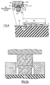
- FIGURE 1 A representation of the general arrangement of an an unassembled package 1 is shown in FIGURE 1.
- This package 1 includes an I/C chip 10 and a card 21 to be joined by C4 bonding.
- Solder bumps 30 are present on the I/O's 11 of the I/C chip 10. These solder bumps 30 on the IC chip 10 correspond to recessed lands 51 on the circuit card 21.
- FIGURE 2 shows an IC chip 10 mounted on a circuit card 21.
- the IC chip 10 is electrically connected and metallurgically bonded to the circuit card 21 by the solder joints 31.
- FIGURE 2 also shows the internal circuitry of the card 21, for example through holes and vias 23, and signal planes and power planes 25.
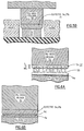
- FIGURE 3 is a cutaway view of an IC chip 10 and card 21 with a reflowed solder ball connector 31.
- the IC chip 10 has an array of I/O leads 11, i.e., contacts 12 on the internal leads 13.
- the individual contacts 12 are surrounded by a passivation layer 14.
- Recessed within the passivation layer 14 are wells with an adhesion layer 15, as a Cr adherence layer 15, and a flash layer 16, as an Au flash layer 16.
- Extending outwardly from the chip 10 is the solder ball 30.
- the solder ball 30 has a characteristic spherical shape because it has been reflowed.
- the circuit card 21 has a eutectic Sn-Pb coated in land 151.
- solder is deposited on solder wettable I/O terminals of the I/C chip 10.
- the solder is deposited from a source of Pb/Sn, such as a molten pool of Pb/Sn solder alloy, containing a cap forming amount of Sn.
- a cap forming amount of Sn is meant an amount of Sn that when the Pb/Sn solder alloy is deposited from the melt or vapor, the resulting as deposited and un-reflowed deposit has a Sn rich cap 37 thereon that is thick enough to form zones and/or regions of Pb/Sn eutectic upon subsequent reflow, thereby obviating the necessity of flux on the IC chip 10 and of electroplated Pb/Sn 151 on the card 21.
- a Sn-rich cap 37 is meant a cap 37 that is in excess of 12.7 ⁇ m (0.5 mil) thick upon deposition and solidification, and contains in excess of 73.1 atomic percent Sn ( 61.9 weight percent Sn) upon deposition and solidification.
- solder is initially deposited on the I/O terminals 11 of the I/C chip 10 so as to form an inhomogeneous, anisotropic column 33 having a relatively Pb-rich core 35 and a relatively Sn-rich cap 37.
- solder wettable I/O terminals 51 there is a matching footprint of solder wettable I/O terminals 51 on the microelectronic circuit card 21.
- the solder wettable I/O terminals 51 are substantially free of deposited solder alloy surface 151, and present a Cu surface 51, or optionally a surface 53 of Cu and oxidation inhibitor.
- FIGURE 4 is a cutaway view, of an IC chip 10 and card 21 with a nonreflowed solder column connector 33, and a Cu land 53.
- the IC chip 10 also has an array of contacts 11 on the internal leads 12. The individual contacts 11 are surrounded by a passivation layer 14. Recessed within the passivation layer are wells with an adhesion layer 15, as a Cr adhesion layer 15, and a flash layer 16, as an Au flash layer 16. Extending outwardly from the chip 10 is the solder column 33. This solder column 33 has not been reflowed, melted, or remelted.
- the circuit card 21 has copper coated lands 53 corresponding to the solder columns 33 on the IC chip 10.
- the height of the solder column 33, combined with the increased via height at the land site 51 on the card 21 provides increased mechanical reliability.
- FIGURE 5A is a schematic representation of the IC chip 10, with the compositionally anisotropic solder column 33, including the Pb rich core 35 and the Sn rich cap 37 during alignment and prior to melting and connecting.
- the solder column 33 which has not previously been reflowed, is now reflowed to form a Pb/Sn eutectic and bond the chip 10 to the microelectronic circuit card 21 (FIGURE 5B).
- FIGURE 5B is a schematic representation of the IC chip 10, including the solder column 33, and the Cu plated 53 card land 51 of FIGURE 5A after reflowing the solder column 33.
- Reflowing is carried out at a temperature in excess of the Pb/Sn eutectic temperature, 183 degrees C. Heating may be carried out by vapor phase heating.
- Bonding occurs by the formation of the Pb/Sn eutectic alloy at the Pb rich core 35 - Sn rich cap 37 interface.
- the Sn rich cap 37 interacts with the Pb rich core 35 of the solder column 31 to form the Sn/Pb eutectic.
- the Pb/Sn eutectic is 26.1 atomic percent Pb (38.1 weight percent Pb), and its formation is favored by the large amount of Sn in proximity to the Pb, that is, by Sn in the Sn rich cap 37 in proximity to the Pb in the Pb rich core 35.
- the size of the Sn rich cap 37 can be enhanced by the use of an alloy with a high nominal Sn concentration, that is, 6 atomic percent or more Sn, basis total Sn and Pb.
- the reflowing step of the process of the invention can be carried out without flux. This is because the thin layer of Sn oxide that forms over the Sn rich cap 37 dissolves in the eutectic solder. Fluxless reflowing obviates the need for organic solvents to remove the flux.
- the lands 51 are free of plated solder 151, not requiring any Sn/Pb electroplate.
- the Sn rich cap 37 serves as the Sn supply for eutectic formation, thereby obviating the need for a Pb/Sn electroplate 151 on the card lands 51.
- an anti-oxidant or corrosion inhibitor such as Entek may be applied to the lands 51.
- FIGURES 6A and 6B An alternative exemplification of the invention is shown in FIGURES 6A and 6B.
- dendrites 55 are present on the card lands 51 prior to melting and connecting.
- These dendrites 55 which may be formed of Cu, Pd, and Cu-Pd alloys, form a reversible mechanical connection prior to reflow. This allows electrical test and burn-in of the IC chip 10 and card 21 without the necessity for solder rework should chip rework be necessary.
- the dendrites 55 can be formed by various methods, such as electroplating, electroless plating, vapor deposition, or the like.
- the package 1 is then assembled by placing the non-reflowed columns 33 directly on the dendritic pads 53.
- the dendrites 55 pierce the Sn rich caps 37 of the solder columns 33 to provide mechanical and electrical interconnection. Electrical testing and IC chip "burn in” can then be performed.
- the IC chips 10 can be removed and replaced if needed. Temporary dendrite bonding is feasible because of the mechanical connection, and because no flux is required for reflow.
- FIGURE 6B is a schematic representation of the IC chip 10, solder column 33, and card land 53 of FIGURE 6A after melting and connecting.
- the method of the invention results in the fabrication of high electronic packages through controlled chip collapse connection direct chip attach.
- the direct chip attach method of the invention has a reduced number of steps, and includes, among other expedients, eliminating the plating of solder onto the card, and eliminating fluxing the solder on the IC chips during attach of the chips to the carrier, as well as eliminating reflowing the solder on the IC chips. These aspects of the invention not only reduce the number of steps in direct chip attach but also provide improved metallurgy.
Landscapes
- Engineering & Computer Science (AREA)
- Manufacturing & Machinery (AREA)
- Microelectronics & Electronic Packaging (AREA)
- Mechanical Engineering (AREA)
- Wire Bonding (AREA)
Applications Claiming Priority (2)
| Application Number | Priority Date | Filing Date | Title |
|---|---|---|---|
| US07/608,766 US5075965A (en) | 1990-11-05 | 1990-11-05 | Low temperature controlled collapse chip attach process |
| US608766 | 1990-11-05 |
Publications (1)
| Publication Number | Publication Date |
|---|---|
| EP0485760A1 true EP0485760A1 (fr) | 1992-05-20 |
Family
ID=24437892
Family Applications (1)
| Application Number | Title | Priority Date | Filing Date |
|---|---|---|---|
| EP91117796A Withdrawn EP0485760A1 (fr) | 1990-11-05 | 1991-10-18 | Procédé d'attachement d'une pièce à écroulement contrôlé à basse température |
Country Status (3)
| Country | Link |
|---|---|
| US (1) | US5075965A (fr) |
| EP (1) | EP0485760A1 (fr) |
| JP (1) | JPH04273453A (fr) |
Cited By (3)
| Publication number | Priority date | Publication date | Assignee | Title |
|---|---|---|---|---|
| EP0675531A3 (fr) * | 1994-03-28 | 1996-07-10 | Bosch Gmbh Robert | Procédé d'interconnection électrique de contacts. |
| EP0704895A3 (fr) * | 1994-09-30 | 1996-12-04 | Nec Corp | Procédé de fabrication d'un dispositif semi-conducteur et d'un substrat semi-conducteur |
| EP0850490B1 (fr) * | 1995-09-08 | 2007-11-07 | Fraunhofer-Gesellschaft zur Förderung der angewandten Forschung e.V. | Procede et dispositif permettant de verifier une puce |
Families Citing this family (85)
| Publication number | Priority date | Publication date | Assignee | Title |
|---|---|---|---|---|
| US5367765A (en) * | 1990-08-31 | 1994-11-29 | Nec Corporation | Method of fabricating integrated circuit chip package |
| US5279711A (en) * | 1991-07-01 | 1994-01-18 | International Business Machines Corporation | Chip attach and sealing method |
| JP3215424B2 (ja) * | 1992-03-24 | 2001-10-09 | ユニシス・コーポレイション | 微細自己整合特性を有する集積回路モジュール |
| US5406701A (en) * | 1992-10-02 | 1995-04-18 | Irvine Sensors Corporation | Fabrication of dense parallel solder bump connections |
| US5480835A (en) * | 1993-05-06 | 1996-01-02 | Motorola, Inc. | Electrical interconnect and method for forming the same |
| US5523696A (en) * | 1993-06-14 | 1996-06-04 | International Business Machines Corp. | Method and apparatus for testing integrated circuit chips |
| JPH07122594A (ja) * | 1993-10-28 | 1995-05-12 | Hitachi Ltd | 導電性バンプの形成方法 |
| US5591941A (en) * | 1993-10-28 | 1997-01-07 | International Business Machines Corporation | Solder ball interconnected assembly |
| US5446625A (en) * | 1993-11-10 | 1995-08-29 | Motorola, Inc. | Chip carrier having copper pattern plated with gold on one surface and devoid of gold on another surface |
| KR100322177B1 (ko) | 1993-12-27 | 2002-05-13 | 이누이 도모지 | 내연기관용점화장치 |
| US5523920A (en) * | 1994-01-03 | 1996-06-04 | Motorola, Inc. | Printed circuit board comprising elevated bond pads |
| US5466635A (en) * | 1994-06-02 | 1995-11-14 | Lsi Logic Corporation | Process for making an interconnect bump for flip-chip integrated circuit including integral standoff and hourglass shaped solder coating |
| US5540377A (en) * | 1994-07-15 | 1996-07-30 | Ito; Carl T. | Solder ball placement machine |
| US5542174A (en) * | 1994-09-15 | 1996-08-06 | Intel Corporation | Method and apparatus for forming solder balls and solder columns |
| DE19524739A1 (de) * | 1994-11-17 | 1996-05-23 | Fraunhofer Ges Forschung | Kernmetall-Lothöcker für die Flip-Chip-Technik |
| JP3138159B2 (ja) * | 1994-11-22 | 2001-02-26 | シャープ株式会社 | 半導体装置、半導体装置実装体、及び半導体装置の交換方法 |
| US5816478A (en) * | 1995-06-05 | 1998-10-06 | Motorola, Inc. | Fluxless flip-chip bond and a method for making |
| US5796591A (en) * | 1995-06-07 | 1998-08-18 | International Business Machines Corporation | Direct chip attach circuit card |
| EP0747954A3 (fr) * | 1995-06-07 | 1997-05-07 | Ibm | Boule de brasure comprenant une couverture métallique à bas point de fusion |
| US6344234B1 (en) | 1995-06-07 | 2002-02-05 | International Business Machines Corportion | Method for forming reflowed solder ball with low melting point metal cap |
| US5634268A (en) * | 1995-06-07 | 1997-06-03 | International Business Machines Corporation | Method for making direct chip attach circuit card |
| US5985692A (en) * | 1995-06-07 | 1999-11-16 | Microunit Systems Engineering, Inc. | Process for flip-chip bonding a semiconductor die having gold bump electrodes |
| JPH0945805A (ja) * | 1995-07-31 | 1997-02-14 | Fujitsu Ltd | 配線基板、半導体装置及び半導体装置を配線基板から取り外す方法並びに半導体装置の製造方法 |
| US6008071A (en) * | 1995-09-20 | 1999-12-28 | Fujitsu Limited | Method of forming solder bumps onto an integrated circuit device |
| EP0789391A3 (fr) | 1996-02-08 | 1998-01-07 | Zevatech, Incorporated | Procédé et dispositif pour l'application de flux, de pâte ou d'adhésif à des interconnexions en réseau de bosses |
| US5729896A (en) * | 1996-10-31 | 1998-03-24 | International Business Machines Corporation | Method for attaching a flip chip on flexible circuit carrier using chip with metallic cap on solder |
| US6336262B1 (en) | 1996-10-31 | 2002-01-08 | International Business Machines Corporation | Process of forming a capacitor with multi-level interconnection technology |
| US5775569A (en) * | 1996-10-31 | 1998-07-07 | Ibm Corporation | Method for building interconnect structures by injection molded solder and structures built |
| US5808853A (en) * | 1996-10-31 | 1998-09-15 | International Business Machines Corporation | Capacitor with multi-level interconnection technology |
| US5996222A (en) * | 1997-01-16 | 1999-12-07 | Ford Motor Company | Soldering process with minimal thermal impact on substrate |
| US6157870A (en) * | 1997-02-18 | 2000-12-05 | Zevatech Trading Ag | Apparatus supplying components to a placement machine with splice sensor |
| US6077022A (en) * | 1997-02-18 | 2000-06-20 | Zevatech Trading Ag | Placement machine and a method to control a placement machine |
| US6330967B1 (en) | 1997-03-13 | 2001-12-18 | International Business Machines Corporation | Process to produce a high temperature interconnection |
| US5953623A (en) * | 1997-04-10 | 1999-09-14 | International Business Machines Corporation | Ball limiting metal mask and tin enrichment of high melting point solder for low temperature interconnection |
| US6043429A (en) * | 1997-05-08 | 2000-03-28 | Advanced Micro Devices, Inc. | Method of making flip chip packages |
| US6025649A (en) * | 1997-07-22 | 2000-02-15 | International Business Machines Corporation | Pb-In-Sn tall C-4 for fatigue enhancement |
| US6335222B1 (en) * | 1997-09-18 | 2002-01-01 | Tessera, Inc. | Microelectronic packages with solder interconnections |
| US5965944A (en) * | 1997-11-12 | 1999-10-12 | International Business Machines Corporation | Printed circuit boards for mounting a semiconductor integrated circuit die |
| US6235996B1 (en) * | 1998-01-28 | 2001-05-22 | International Business Machines Corporation | Interconnection structure and process module assembly and rework |
| US6423623B1 (en) | 1998-06-09 | 2002-07-23 | Fairchild Semiconductor Corporation | Low Resistance package for semiconductor devices |
| US6133634A (en) | 1998-08-05 | 2000-10-17 | Fairchild Semiconductor Corporation | High performance flip chip package |
| US6194667B1 (en) | 1998-08-19 | 2001-02-27 | International Business Machines Corporation | Receptor pad structure for chip carriers |
| JP3960445B2 (ja) * | 1998-10-12 | 2007-08-15 | 新光電気工業株式会社 | 半導体装置とその製造方法 |
| US6552425B1 (en) * | 1998-12-18 | 2003-04-22 | Intel Corporation | Integrated circuit package |
| US6427901B2 (en) * | 1999-06-30 | 2002-08-06 | Lucent Technologies Inc. | System and method for forming stable solder bonds |
| US6570251B1 (en) * | 1999-09-02 | 2003-05-27 | Micron Technology, Inc. | Under bump metalization pad and solder bump connections |
| CA2313551A1 (fr) | 1999-10-21 | 2001-04-21 | International Business Machines Corporation | Anneau de support rigide integre a une tranche |
| US6420207B1 (en) * | 2000-01-04 | 2002-07-16 | Multek Hong Kong Limited | Semiconductor package and enhanced FBG manufacturing |
| US6469394B1 (en) | 2000-01-31 | 2002-10-22 | Fujitsu Limited | Conductive interconnect structures and methods for forming conductive interconnect structures |
| US6592019B2 (en) | 2000-04-27 | 2003-07-15 | Advanpack Solutions Pte. Ltd | Pillar connections for semiconductor chips and method of manufacture |
| US6578754B1 (en) * | 2000-04-27 | 2003-06-17 | Advanpack Solutions Pte. Ltd. | Pillar connections for semiconductor chips and method of manufacture |
| US6378759B1 (en) * | 2000-07-18 | 2002-04-30 | Chartered Semiconductor Manufacturing Ltd. | Method of application of conductive cap-layer in flip-chip, COB, and micro metal bonding |
| JP3822040B2 (ja) * | 2000-08-31 | 2006-09-13 | 株式会社ルネサステクノロジ | 電子装置及びその製造方法 |
| US6931723B1 (en) | 2000-09-19 | 2005-08-23 | International Business Machines Corporation | Organic dielectric electronic interconnect structures and method for making |
| JP2002134545A (ja) * | 2000-10-26 | 2002-05-10 | Oki Electric Ind Co Ltd | 半導体集積回路チップ及び基板、並びにその製造方法 |
| TWI313507B (en) * | 2002-10-25 | 2009-08-11 | Megica Corporatio | Method for assembling chips |
| US6818545B2 (en) * | 2001-03-05 | 2004-11-16 | Megic Corporation | Low fabrication cost, fine pitch and high reliability solder bump |
| US20060163729A1 (en) * | 2001-04-18 | 2006-07-27 | Mou-Shiung Lin | Structure and manufacturing method of a chip scale package |
| US7067916B2 (en) * | 2001-06-20 | 2006-06-27 | International Business Machines Corporation | Extension of fatigue life for C4 solder ball to chip connection |
| JP4105409B2 (ja) * | 2001-06-22 | 2008-06-25 | 株式会社ルネサステクノロジ | マルチチップモジュールの製造方法 |
| TWI245402B (en) | 2002-01-07 | 2005-12-11 | Megic Corp | Rod soldering structure and manufacturing process thereof |
| US6877653B2 (en) * | 2002-02-27 | 2005-04-12 | Advanced Semiconductor Engineering, Inc. | Method of modifying tin to lead ratio in tin-lead bump |
| US20030234276A1 (en) * | 2002-06-20 | 2003-12-25 | Ultratera Corporation | Strengthened bonding mechanism for semiconductor package |
| US7026233B2 (en) * | 2003-08-06 | 2006-04-11 | Taiwan Semiconductor Manufacturing Company, Ltd. | Method for reducing defects in post passivation interconnect process |
| TWI221343B (en) * | 2003-10-21 | 2004-09-21 | Advanced Semiconductor Eng | Wafer structure for preventing contamination of bond pads during SMT process and process for the same |
| US8294279B2 (en) | 2005-01-25 | 2012-10-23 | Megica Corporation | Chip package with dam bar restricting flow of underfill |
| KR100790978B1 (ko) * | 2006-01-24 | 2008-01-02 | 삼성전자주식회사 | 저온에서의 접합 방법, 및 이를 이용한 반도체 패키지 실장 방법 |
| FR2897503B1 (fr) * | 2006-02-16 | 2014-06-06 | Valeo Sys Controle Moteur Sas | Procede de fabrication d'un module electronique par fixation sequentielle des composants et ligne de production correspondante |
| US20070284420A1 (en) * | 2006-06-13 | 2007-12-13 | Advanpack Solutions Pte Ltd | Integrated circuit chip formed on substrate |
| US7600667B2 (en) * | 2006-09-29 | 2009-10-13 | Intel Corporation | Method of assembling carbon nanotube reinforced solder caps |
| US20080160751A1 (en) * | 2006-12-28 | 2008-07-03 | Mengzhi Pang | Microelectronic die including solder caps on bumping sites thereof and method of making same |
| AT10735U1 (de) * | 2008-05-21 | 2009-09-15 | Austria Tech & System Tech | Verfahren zur herstellung einer leiterplatte sowie verwendung und leiterplatte |
| DE102008025833A1 (de) | 2008-05-29 | 2009-12-17 | Fraunhofer-Gesellschaft zur Förderung der angewandten Forschung e.V. | Verfahren und Vorrichtung zum stoffschlüssigen Fügen metallischer Anschlussstrukturen |
| WO2010066366A1 (fr) * | 2008-12-13 | 2010-06-17 | Muehlbauer Ag | Procédé et appareil de fabrication d'un ensemble électronique, ensemble électronique fabriqué par le procédé ou dans l'appareil |
| US9142533B2 (en) * | 2010-05-20 | 2015-09-22 | Taiwan Semiconductor Manufacturing Company, Ltd. | Substrate interconnections having different sizes |
| US9252094B2 (en) | 2011-04-30 | 2016-02-02 | Stats Chippac, Ltd. | Semiconductor device and method of forming an interconnect structure with conductive material recessed within conductive ring over surface of conductive pillar |
| US9646923B2 (en) | 2012-04-17 | 2017-05-09 | Taiwan Semiconductor Manufacturing Company, Ltd. | Semiconductor devices, methods of manufacture thereof, and packaged semiconductor devices |
| US9425136B2 (en) | 2012-04-17 | 2016-08-23 | Taiwan Semiconductor Manufacturing Company, Ltd. | Conical-shaped or tier-shaped pillar connections |
| US9299674B2 (en) | 2012-04-18 | 2016-03-29 | Taiwan Semiconductor Manufacturing Company, Ltd. | Bump-on-trace interconnect |
| US9111817B2 (en) | 2012-09-18 | 2015-08-18 | Taiwan Semiconductor Manufacturing Company, Ltd. | Bump structure and method of forming same |
| TWI582929B (zh) * | 2016-06-07 | 2017-05-11 | 南茂科技股份有限公司 | 晶片封裝結構 |
| US10217712B2 (en) * | 2016-12-16 | 2019-02-26 | Advanced Semiconductor Engineering, Inc. | Semiconductor package and semiconductor process for manufacturing the same |
| CN109824011A (zh) * | 2017-11-23 | 2019-05-31 | 上海新微技术研发中心有限公司 | 一种共晶键合的结构和方法 |
| CN112186086B (zh) * | 2019-06-17 | 2022-01-25 | 成都辰显光电有限公司 | 微型发光二极管芯片的键合方法 |
| DE102021103360A1 (de) * | 2021-02-05 | 2022-08-11 | Few Fahrzeugelektrik Werk Gmbh & Co. Kg | Verfahren zur Herstellung einer Vorverzinnungsanordnung und derartige Vorverzinnungsanordnung |
Citations (1)
| Publication number | Priority date | Publication date | Assignee | Title |
|---|---|---|---|---|
| EP0177042A2 (fr) * | 1984-10-05 | 1986-04-09 | Hitachi, Ltd. | Dispositif de circuit semi-conducteur et son procédé de fabrication |
Family Cites Families (6)
| Publication number | Priority date | Publication date | Assignee | Title |
|---|---|---|---|---|
| DE258314C (fr) * | 1912-04-23 | 1913-04-02 | ||
| US3716421A (en) * | 1971-03-19 | 1973-02-13 | Gte Sylvania Inc | Compositions for improved solderability of copper |
| US4373656A (en) * | 1981-07-17 | 1983-02-15 | Western Electric Company, Inc. | Method of preserving the solderability of copper |
| JPS6214433A (ja) * | 1985-07-12 | 1987-01-23 | Hitachi Ltd | 電子回路装置およびその製造方法 |
| US4731128A (en) * | 1987-05-21 | 1988-03-15 | International Business Machines Corporation | Protection of copper from corrosion |
| US4967950A (en) * | 1989-10-31 | 1990-11-06 | International Business Machines Corporation | Soldering method |
-
1990
- 1990-11-05 US US07/608,766 patent/US5075965A/en not_active Expired - Fee Related
-
1991
- 1991-10-03 JP JP3281962A patent/JPH04273453A/ja active Pending
- 1991-10-18 EP EP91117796A patent/EP0485760A1/fr not_active Withdrawn
Patent Citations (1)
| Publication number | Priority date | Publication date | Assignee | Title |
|---|---|---|---|---|
| EP0177042A2 (fr) * | 1984-10-05 | 1986-04-09 | Hitachi, Ltd. | Dispositif de circuit semi-conducteur et son procédé de fabrication |
Non-Patent Citations (3)
| Title |
|---|
| IBM TECHNICAL DISCLOSURE BULLETIN. vol. 32, no. 6B, November 1989, NEW YORK US page 180; 'Process forForming a High-aspect-ratio solder interconnection' * |
| INTERNATIONAL JOURNAL FOR HYBRID MICROELECTRONICS. vol. 13, no. 3, September 1990, SILVER SPRING MD US pages 69 - 84; YAMAKAWA ET AL: 'Maskless Bumping by Electroless Plating for High Pin Count, Thin, and Low Cost Microcircuits' * |
| RELIABILITY PHYSICS 1982 - 20TH ANNUAL PROCEEDINGS vol. 20, 30 March 1982, NEW YORK,US pages 194 - 201; YOUNG AND DE MIRANDA: 'Analytical techniques for controlled collapse bump structures' * |
Cited By (5)
| Publication number | Priority date | Publication date | Assignee | Title |
|---|---|---|---|---|
| EP0675531A3 (fr) * | 1994-03-28 | 1996-07-10 | Bosch Gmbh Robert | Procédé d'interconnection électrique de contacts. |
| EP0704895A3 (fr) * | 1994-09-30 | 1996-12-04 | Nec Corp | Procédé de fabrication d'un dispositif semi-conducteur et d'un substrat semi-conducteur |
| US5844304A (en) * | 1994-09-30 | 1998-12-01 | Nec Corporation | Process for manufacturing semiconductor device and semiconductor wafer |
| USRE39603E1 (en) * | 1994-09-30 | 2007-05-01 | Nec Corporation | Process for manufacturing semiconductor device and semiconductor wafer |
| EP0850490B1 (fr) * | 1995-09-08 | 2007-11-07 | Fraunhofer-Gesellschaft zur Förderung der angewandten Forschung e.V. | Procede et dispositif permettant de verifier une puce |
Also Published As
| Publication number | Publication date |
|---|---|
| JPH04273453A (ja) | 1992-09-29 |
| US5075965A (en) | 1991-12-31 |
Similar Documents
| Publication | Publication Date | Title |
|---|---|---|
| US5075965A (en) | Low temperature controlled collapse chip attach process | |
| US6121069A (en) | Interconnect structure for joining a chip to a circuit card | |
| US5873512A (en) | Application of low temperature metallurgical paste to form a bond structure to attach an electronic component to a carrier | |
| US5796591A (en) | Direct chip attach circuit card | |
| US6994243B2 (en) | Low temperature solder chip attach structure and process to produce a high temperature interconnection | |
| US5634268A (en) | Method for making direct chip attach circuit card | |
| US5874043A (en) | Lead-free, high tin ternary solder alloy of tin, silver, and indium | |
| US6013571A (en) | Microelectronic assembly including columnar interconnections and method for forming same | |
| US6307160B1 (en) | High-strength solder interconnect for copper/electroless nickel/immersion gold metallization solder pad and method | |
| US5672542A (en) | Method of making solder balls by contained paste deposition | |
| JP3300839B2 (ja) | 半導体素子ならびにその製造および使用方法 | |
| US6158644A (en) | Method for enhancing fatigue life of ball grid arrays | |
| US6025649A (en) | Pb-In-Sn tall C-4 for fatigue enhancement | |
| US5274913A (en) | Method of fabricating a reworkable module | |
| US6127735A (en) | Interconnect for low temperature chip attachment | |
| KR20010112057A (ko) | 반도체 모듈 및 반도체 장치를 접속한 회로 기판 | |
| US5631447A (en) | Uses of uniaxially electrically conductive articles | |
| US5646068A (en) | Solder bump transfer for microelectronics packaging and assembly | |
| EP0329314A1 (fr) | Utilisation d'articles électroconducteurs uni-axiaux | |
| US6127731A (en) | Capped solder bumps which form an interconnection with a tailored reflow melting point | |
| US5759285A (en) | Method and solution for cleaning solder connections of electronic components | |
| KR980013565A (ko) | C-4 피로 수명 개선용 삼원 솔더 | |
| WO1997047425A1 (fr) | Alliage de soudage ternaire sans plomb a teneur elevee en etain constitue d'etain, d'argent et de bismuth | |
| JP2894172B2 (ja) | 半導体装置 |
Legal Events
| Date | Code | Title | Description |
|---|---|---|---|
| PUAI | Public reference made under article 153(3) epc to a published international application that has entered the european phase |
Free format text: ORIGINAL CODE: 0009012 |
|
| AK | Designated contracting states |
Kind code of ref document: A1 Designated state(s): DE FR GB |
|
| STAA | Information on the status of an ep patent application or granted ep patent |
Free format text: STATUS: THE APPLICATION IS DEEMED TO BE WITHDRAWN |
|
| 18D | Application deemed to be withdrawn |
Effective date: 19921121 |