EP0485850A2 - Procédé et dispositif de mesure de l'atténuation d'un médium optique - Google Patents
Procédé et dispositif de mesure de l'atténuation d'un médium optique Download PDFInfo
- Publication number
- EP0485850A2 EP0485850A2 EP91118785A EP91118785A EP0485850A2 EP 0485850 A2 EP0485850 A2 EP 0485850A2 EP 91118785 A EP91118785 A EP 91118785A EP 91118785 A EP91118785 A EP 91118785A EP 0485850 A2 EP0485850 A2 EP 0485850A2
- Authority
- EP
- European Patent Office
- Prior art keywords
- transmitter
- receiver
- measurements
- measuring
- transmitters
- Prior art date
- Legal status (The legal status is an assumption and is not a legal conclusion. Google has not performed a legal analysis and makes no representation as to the accuracy of the status listed.)
- Granted
Links
Images

Classifications
-
- G—PHYSICS
- G01—MEASURING; TESTING
- G01M—TESTING STATIC OR DYNAMIC BALANCE OF MACHINES OR STRUCTURES; TESTING OF STRUCTURES OR APPARATUS, NOT OTHERWISE PROVIDED FOR
- G01M11/00—Testing of optical apparatus; Testing structures by optical methods not otherwise provided for
- G01M11/30—Testing of optical devices, constituted by fibre optics or optical waveguides
- G01M11/33—Testing of optical devices, constituted by fibre optics or optical waveguides with a light emitter being disposed at one fibre or waveguide end-face, and a light receiver at the other end-face
-
- G—PHYSICS
- G01—MEASURING; TESTING
- G01M—TESTING STATIC OR DYNAMIC BALANCE OF MACHINES OR STRUCTURES; TESTING OF STRUCTURES OR APPARATUS, NOT OTHERWISE PROVIDED FOR
- G01M11/00—Testing of optical apparatus; Testing structures by optical methods not otherwise provided for
- G01M11/30—Testing of optical devices, constituted by fibre optics or optical waveguides
- G01M11/35—Testing of optical devices, constituted by fibre optics or optical waveguides in which light is transversely coupled into or out of the fibre or waveguide, e.g. using integrating spheres
Definitions
- the invention relates to a method for measuring the optical attenuation of an optical medium using two measuring transmitters and two receivers which are arranged on both sides of the optical medium, the transmitters and the receivers being coupled to an optical waveguide in each case and measurements from both sides of the optical medium be performed.
- Measuring methods in which bending couplers are used are e.g. described in DE-OS 38 28 604 and in US-PS 4,652,123. As is explained in detail there, particularly exact results can be achieved when working with two transmitters and two receivers and successively carrying out several measurements starting from both sides of the measurement object.
- a particularly advantageous development of the invention is that a new measured value is formed by interpolation from two successive measured values of a series of measurements, each of which goes back to a transmitter, and that this measured value found by interpolation for the calculation of the damping is the time between the first two measured values the measured value obtained from the other transmitter is assigned.
- a synthetic measured value is generated, the amplitude value of which corresponds almost exactly to the value that could be obtained from a completely simultaneous measurement with both measuring transmitters.
- the error is only determined by the difference that the curvature offers compared to the straight-line interpolation. This is largely irrelevant for the short time intervals with which measurements are made.
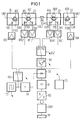
- a measuring device is drawn in a schematic representation, which is used to carry out the inventive method.
- An optical medium OM to be measured for example a splice, a piece of optical fiber of greater length, an optical cable or the like is connected on the left and right to two optical fibers LW1 and LW2.
- An optical transmitter SL is provided to the left of the optical medium, the transmitter diode of which is designated SDL.
- an optical transmitter SR on the right-hand side, the transmitter diode of which is designated SDR.
- an optical receiver EL which has two receiving diodes EDR2 and EDL2.
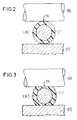
- the light emerging from the optical waveguide LW2 due to the bend is received by the two receiving diodes EDR1 (coming from the right) and EDL1 (coming from the left). These two photodiodes EDR1 and EDL1 are arranged spatially fixed in the coupling area and are dimensioned and aligned so that they absorb as much of the emerging light as possible.
- the optimization of the light-sensitive receiving device in the receivers ER and EL is thus designed for the final state, that is, in a transition region in which the deformation of the coating of the optical waveguide has not yet been completed, less light is absorbed than in the final state.
- the circuit elements indicated as block diagrams in the lower part of FIG. 1 are used for the processing of the transmit signals and the evaluation of the received signals.
- an oscillator (clock generator) OS is shown here, which supplies the control signal for the transmit diode drivers VSL and VSR.
- a changeover switch US1 is provided, which optionally supplies the clock signal to the transmission driver VSL of the left transmitter SL and VSR of the right transmitter SR.
- the changeover switch US is controlled by a central control element CS, which is expediently synchronized with the clock of the clock generator OS or synchronizes it (here, as indicated by an arrow in the other circuit parts US1 and US2).
- the oscillator OS can be omitted.
- the transmit diode driver stages VSL and VSR control the transmit diodes SDL and SDR, the driver circuit regulating their transmit power when using laser diodes.
- 1300 nm light-emitting diodes can be used as transmission diodes SDL and SDR.
- the transmission power is to a certain extent temperature-dependent and therefore also time-dependent due to the power loss of the diodes. If laser diodes are used for SDL and SDR, which contain a built-in monitor diode, this time dependency on the transmitter side can be compensated by an appropriate control by means of a power control.
- the adjustable preamplifier VV is followed by a synchronous rectifier SD.
- a synchronous rectifier SD This is useful because a modulated transmission signal is advantageously used to avoid problems with extraneous light, dark currents and drift.
- This signal detection by a phase-sensitive rectifier (synchronous rectifier) causes optimal interference suppression so that a very high sensitivity is achieved.
- the synchronous rectifier SD is driven by the clock generator OS, specifically via a delay element (phase shifter) SG. The phase shift generated in this way is used to compensate for the signal propagation time.
Landscapes
- Physics & Mathematics (AREA)
- Optics & Photonics (AREA)
- Chemical & Material Sciences (AREA)
- Analytical Chemistry (AREA)
- General Physics & Mathematics (AREA)
- Investigating Or Analysing Materials By Optical Means (AREA)
- Arrangements For Transmission Of Measured Signals (AREA)
- Measurement Of The Respiration, Hearing Ability, Form, And Blood Characteristics Of Living Organisms (AREA)
Applications Claiming Priority (2)
| Application Number | Priority Date | Filing Date | Title |
|---|---|---|---|
| DE4036074 | 1990-11-13 | ||
| DE4036074 | 1990-11-13 |
Publications (3)
| Publication Number | Publication Date |
|---|---|
| EP0485850A2 true EP0485850A2 (fr) | 1992-05-20 |
| EP0485850A3 EP0485850A3 (en) | 1993-02-24 |
| EP0485850B1 EP0485850B1 (fr) | 1995-07-19 |
Family
ID=6418163
Family Applications (1)
| Application Number | Title | Priority Date | Filing Date |
|---|---|---|---|
| EP91118785A Expired - Lifetime EP0485850B1 (fr) | 1990-11-13 | 1991-11-04 | Procédé et dispositif de mesure de l'atténuation d'un médium optique |
Country Status (4)
| Country | Link |
|---|---|
| US (1) | US5189300A (fr) |
| EP (1) | EP0485850B1 (fr) |
| AT (1) | ATE125355T1 (fr) |
| DE (1) | DE59106029D1 (fr) |
Families Citing this family (4)
| Publication number | Priority date | Publication date | Assignee | Title |
|---|---|---|---|---|
| EP0576969A1 (fr) * | 1992-07-01 | 1994-01-05 | Siemens Aktiengesellschaft | Procédé et dispositif pour introduire un compteur incurvé dans une position de couplage |
| US5357332A (en) * | 1992-08-11 | 1994-10-18 | Photonix Industries | Apparatus for, and method of, determining the effectiveness of a splice of optical fiber |
| US5334832A (en) * | 1993-06-15 | 1994-08-02 | Photonix Industries | Apparatus and methods for determining splice effectiveness between two optical fibers using solid gels as coupling enhancers for measuring component attenuation |
| DE19917751C2 (de) * | 1999-04-20 | 2001-05-31 | Nokia Networks Oy | Verfahren und Überwachungsvorrichtung zur Überwachung der Qualität der Datenübertragung über analoge Leitungen |
Family Cites Families (4)
| Publication number | Priority date | Publication date | Assignee | Title |
|---|---|---|---|---|
| US4183666A (en) * | 1977-03-10 | 1980-01-15 | Mitsubishi Rayon Company, Limited | Method of measuring light transmission losses of optical materials |
| US4664732A (en) * | 1981-04-27 | 1987-05-12 | Raychem Corp. | Methods and apparatus for optical fiber systems |
| CA1213057A (fr) * | 1984-10-25 | 1986-10-21 | Northern Telecom Limited | Methode et instrument de mesure de la dissipation absolue au site d'accouplement de fibres |
| DE3828604A1 (de) * | 1988-08-23 | 1990-03-01 | Siemens Ag | Verfahren und einrichtung zur messung der optischen daempfung eines optischen mediums |
-
1991
- 1991-10-28 US US07/783,401 patent/US5189300A/en not_active Expired - Fee Related
- 1991-11-04 DE DE59106029T patent/DE59106029D1/de not_active Expired - Fee Related
- 1991-11-04 EP EP91118785A patent/EP0485850B1/fr not_active Expired - Lifetime
- 1991-11-04 AT AT91118785T patent/ATE125355T1/de not_active IP Right Cessation
Also Published As
| Publication number | Publication date |
|---|---|
| DE59106029D1 (de) | 1995-08-24 |
| EP0485850B1 (fr) | 1995-07-19 |
| US5189300A (en) | 1993-02-23 |
| EP0485850A3 (en) | 1993-02-24 |
| ATE125355T1 (de) | 1995-08-15 |
Similar Documents
| Publication | Publication Date | Title |
|---|---|---|
| DE3029716C2 (de) | Verfahren und Vorrichtung zur automatischen Aufrechterhaltung einer Justage der Deckung und der relativen Phasenlage von Lichtstrahlen in einem für den Ultraschallempfang benutzten optischen Interferometer | |
| EP0742450B1 (fr) | Procédé et dispositif de mesure du temps de vol de lumière le long d'une trajectoire de mesure entre un dispositif de mesure et un objet réfléchissant | |
| DE60100064T2 (de) | Bestimmung der Eigenschaften eines optischen Gerätes | |
| EP0009220B1 (fr) | Système pour la transmission de signaux par une liaison optique | |
| EP0054292A2 (fr) | Arrangement de mesure fibre-optique | |
| EP0795121A1 (fr) | Procede et dispositif permettant de mesurer des faisceaux lumineux | |
| DE102007059551A1 (de) | Einrichtung zur Messung der Eigenschaften einer Lichtleitfaser | |
| DE2652608B2 (de) | Anordnung zur Regelung der Ausgangsleistung eines Halbleiterlasers | |
| EP0010682A1 (fr) | Dispositif pour la transmission de signaux analogique par une liaison optique | |
| DE3514647C2 (fr) | ||
| DE4240721A1 (de) | Meßverfahren und Meßvorrichtung mit analoger optischer Signalübertragung | |
| WO2021032387A1 (fr) | Unité d'alignement, module de détection comprenant cette unité d'alignement et système d'usinage au laser comprenant ce module de détection | |
| EP0173155B1 (fr) | Source d'alimentation pour source lumineuse de capteurs optiques à modulation de fréquence | |
| CH697667B1 (de) | Doppelparameter-Laseroptikrückkopplung. | |
| EP1089061B1 (fr) | Microscope à balayage laser et méthode de correction de la référence pour un microscope à balayage laser | |
| DE10029167B4 (de) | Verfahren und Vorrichtung zur Temperaturstabilisierung optischer Bauteile | |
| EP0485850B1 (fr) | Procédé et dispositif de mesure de l'atténuation d'un médium optique | |
| DE19919091A1 (de) | Anordnung zur Einstellung der Laserleistung und/oder der Pulslänge eines Kurzpulslasers in einem Mikroskop | |
| DE102009022953A1 (de) | Verfahren und Anordnung zum Ermitteln der Dehnung oder Stauchung eines faseroptischen Gitters | |
| EP0675351B1 (fr) | Procédé de détermination dans un fibre optique la longeur d'ondes pour laquelle il y n'a pas de dispersion | |
| DE10033269B4 (de) | Vorrichtung zum Einkoppeln von Licht mindestens einer Wellenlänge einer Laserlichtquelle in ein konfokales Rastermikroskop | |
| DE19621794A1 (de) | Bidirektionale, optisch gespeiste Signalübertragungsvorrichtung | |
| DE2846696A1 (de) | Einrichtung zur feststellung der scharfeinstellung | |
| DE60312266T2 (de) | Einphasen-Kipp Verschiebungsverfahren und Apparat zur Messung der chromatischen und polarisationsabhängigen Dispersion. | |
| EP0012179B1 (fr) | Ajustage des extrémités de deux fibres optiques devant être connectées |
Legal Events
| Date | Code | Title | Description |
|---|---|---|---|
| PUAI | Public reference made under article 153(3) epc to a published international application that has entered the european phase |
Free format text: ORIGINAL CODE: 0009012 |
|
| AK | Designated contracting states |
Kind code of ref document: A2 Designated state(s): AT BE CH DE FR GB IT LI NL SE |
|
| PUAL | Search report despatched |
Free format text: ORIGINAL CODE: 0009013 |
|
| AK | Designated contracting states |
Kind code of ref document: A3 Designated state(s): AT BE CH DE FR GB IT LI NL SE |
|
| 17P | Request for examination filed |
Effective date: 19930324 |
|
| 17Q | First examination report despatched |
Effective date: 19940429 |
|
| GRAA | (expected) grant |
Free format text: ORIGINAL CODE: 0009210 |
|
| AK | Designated contracting states |
Kind code of ref document: B1 Designated state(s): AT BE CH DE FR GB IT LI NL SE |
|
| REF | Corresponds to: |
Ref document number: 125355 Country of ref document: AT Date of ref document: 19950815 Kind code of ref document: T |
|
| REF | Corresponds to: |
Ref document number: 59106029 Country of ref document: DE Date of ref document: 19950824 |
|
| ITF | It: translation for a ep patent filed | ||
| GBT | Gb: translation of ep patent filed (gb section 77(6)(a)/1977) |
Effective date: 19950925 |
|
| ET | Fr: translation filed | ||
| PLBE | No opposition filed within time limit |
Free format text: ORIGINAL CODE: 0009261 |
|
| STAA | Information on the status of an ep patent application or granted ep patent |
Free format text: STATUS: NO OPPOSITION FILED WITHIN TIME LIMIT |
|
| 26N | No opposition filed | ||
| PGFP | Annual fee paid to national office [announced via postgrant information from national office to epo] |
Ref country code: AT Payment date: 19991109 Year of fee payment: 9 |
|
| PGFP | Annual fee paid to national office [announced via postgrant information from national office to epo] |
Ref country code: GB Payment date: 19991116 Year of fee payment: 9 |
|
| PGFP | Annual fee paid to national office [announced via postgrant information from national office to epo] |
Ref country code: SE Payment date: 19991118 Year of fee payment: 9 |
|
| PGFP | Annual fee paid to national office [announced via postgrant information from national office to epo] |
Ref country code: NL Payment date: 19991122 Year of fee payment: 9 |
|
| PGFP | Annual fee paid to national office [announced via postgrant information from national office to epo] |
Ref country code: BE Payment date: 19991123 Year of fee payment: 9 |
|
| PGFP | Annual fee paid to national office [announced via postgrant information from national office to epo] |
Ref country code: FR Payment date: 19991126 Year of fee payment: 9 |
|
| PGFP | Annual fee paid to national office [announced via postgrant information from national office to epo] |
Ref country code: DE Payment date: 20000121 Year of fee payment: 9 |
|
| PG25 | Lapsed in a contracting state [announced via postgrant information from national office to epo] |
Ref country code: GB Free format text: LAPSE BECAUSE OF NON-PAYMENT OF DUE FEES Effective date: 20001104 Ref country code: AT Free format text: LAPSE BECAUSE OF NON-PAYMENT OF DUE FEES Effective date: 20001104 |
|
| PG25 | Lapsed in a contracting state [announced via postgrant information from national office to epo] |
Ref country code: SE Free format text: THE PATENT HAS BEEN ANNULLED BY A DECISION OF A NATIONAL AUTHORITY Effective date: 20001129 |
|
| PG25 | Lapsed in a contracting state [announced via postgrant information from national office to epo] |
Ref country code: BE Free format text: LAPSE BECAUSE OF NON-PAYMENT OF DUE FEES Effective date: 20001130 |
|
| PGFP | Annual fee paid to national office [announced via postgrant information from national office to epo] |
Ref country code: CH Payment date: 20001204 Year of fee payment: 10 |
|
| BERE | Be: lapsed |
Owner name: SIEMENS A.G. Effective date: 20001130 |
|
| PG25 | Lapsed in a contracting state [announced via postgrant information from national office to epo] |
Ref country code: NL Free format text: LAPSE BECAUSE OF NON-PAYMENT OF DUE FEES Effective date: 20010601 |
|
| GBPC | Gb: european patent ceased through non-payment of renewal fee |
Effective date: 20001104 |
|
| EUG | Se: european patent has lapsed |
Ref document number: 91118785.4 |
|
| PG25 | Lapsed in a contracting state [announced via postgrant information from national office to epo] |
Ref country code: FR Free format text: LAPSE BECAUSE OF NON-PAYMENT OF DUE FEES Effective date: 20010731 |
|
| NLV4 | Nl: lapsed or anulled due to non-payment of the annual fee |
Effective date: 20010601 |
|
| PG25 | Lapsed in a contracting state [announced via postgrant information from national office to epo] |
Ref country code: DE Free format text: LAPSE BECAUSE OF NON-PAYMENT OF DUE FEES Effective date: 20010801 |
|
| REG | Reference to a national code |
Ref country code: FR Ref legal event code: ST |
|
| PG25 | Lapsed in a contracting state [announced via postgrant information from national office to epo] |
Ref country code: LI Free format text: LAPSE BECAUSE OF NON-PAYMENT OF DUE FEES Effective date: 20011130 Ref country code: CH Free format text: LAPSE BECAUSE OF NON-PAYMENT OF DUE FEES Effective date: 20011130 |
|
| REG | Reference to a national code |
Ref country code: CH Ref legal event code: PL |
|
| PG25 | Lapsed in a contracting state [announced via postgrant information from national office to epo] |
Ref country code: IT Free format text: LAPSE BECAUSE OF NON-PAYMENT OF DUE FEES;WARNING: LAPSES OF ITALIAN PATENTS WITH EFFECTIVE DATE BEFORE 2007 MAY HAVE OCCURRED AT ANY TIME BEFORE 2007. THE CORRECT EFFECTIVE DATE MAY BE DIFFERENT FROM THE ONE RECORDED. Effective date: 20051104 |