EP0486023B1 - Selbstleitweglenkendes Netzwerk mit optischer Gattermatrix - Google Patents
Selbstleitweglenkendes Netzwerk mit optischer Gattermatrix Download PDFInfo
- Publication number
- EP0486023B1 EP0486023B1 EP91119452A EP91119452A EP0486023B1 EP 0486023 B1 EP0486023 B1 EP 0486023B1 EP 91119452 A EP91119452 A EP 91119452A EP 91119452 A EP91119452 A EP 91119452A EP 0486023 B1 EP0486023 B1 EP 0486023B1
- Authority
- EP
- European Patent Office
- Prior art keywords
- optical
- gates
- incident
- packet
- stage
- Prior art date
- Legal status (The legal status is an assumption and is not a legal conclusion. Google has not performed a legal analysis and makes no representation as to the accuracy of the status listed.)
- Expired - Lifetime
Links
- 230000003287 optical effect Effects 0.000 title claims description 307
- 230000008878 coupling Effects 0.000 claims description 4
- 238000010168 coupling process Methods 0.000 claims description 4
- 238000005859 coupling reaction Methods 0.000 claims description 4
- 230000011664 signaling Effects 0.000 claims 1
- 238000010586 diagram Methods 0.000 description 23
- 230000003247 decreasing effect Effects 0.000 description 5
- 230000004048 modification Effects 0.000 description 5
- 238000012986 modification Methods 0.000 description 5
- 230000003111 delayed effect Effects 0.000 description 4
- 230000005284 excitation Effects 0.000 description 4
- 230000005281 excited state Effects 0.000 description 3
- 230000007717 exclusion Effects 0.000 description 3
- 238000005513 bias potential Methods 0.000 description 1
- 230000005540 biological transmission Effects 0.000 description 1
- 238000004891 communication Methods 0.000 description 1
- 239000004020 conductor Substances 0.000 description 1
- 238000005516 engineering process Methods 0.000 description 1
- 238000001914 filtration Methods 0.000 description 1
- 238000003780 insertion Methods 0.000 description 1
- 230000037431 insertion Effects 0.000 description 1
- 239000000463 material Substances 0.000 description 1
- 239000011159 matrix material Substances 0.000 description 1
- 239000004065 semiconductor Substances 0.000 description 1
Images








Classifications
-
- H—ELECTRICITY
- H04—ELECTRIC COMMUNICATION TECHNIQUE
- H04Q—SELECTING
- H04Q11/00—Selecting arrangements for multiplex systems
- H04Q11/0001—Selecting arrangements for multiplex systems using optical switching
- H04Q11/0005—Switch and router aspects
-
- H—ELECTRICITY
- H04—ELECTRIC COMMUNICATION TECHNIQUE
- H04Q—SELECTING
- H04Q11/00—Selecting arrangements for multiplex systems
- H04Q11/0001—Selecting arrangements for multiplex systems using optical switching
- H04Q11/0062—Network aspects
- H04Q11/0066—Provisions for optical burst or packet networks
Definitions
- the present invention relates generally to optical self-routing networks for routing optical packets according to the information contained in the header of the packets.
- optical packet is fed into a splitter in which it is split into two replicas of the input signal, one being applied to an optical switch having two outlet terminals, and the other to an optical correlator.
- the optical correlator generates an optical output if the header of the incoming packet contains a predetermined bit sequence.
- the output of the correlator is converted to an electrical signal, amplified and applied to the control electrode of the optical switch to direct the incident light to one of its outlet terminals.
- the gate control means supplies successively shifted gate control electrical signals respectively to the optical gates of each set so that one of the optical gates of a given set exclusively allows passage of an optical signal incident thereon when the gate control electrical signal applied thereto is the earliest of the gate control electrical signals which are successively applied to the optical gates of the given set.
- the optical gates of each set are commonly assigned a unique time interval, and those of the optical signals which are supplied to the optical gates of each set are successively shifted during the unique time interval.
- the gate control means exclusively causes one of the optical gates of each set to allow passage of an optical signal incident thereon when the incident optical signal is the earliest of the optical signals incident on the optical gates of the set.
- the gate control means simultaneously supplies gate control electrical signals of different amplitudes respectively to the optical gates of each set so that one of the optical gates of a given set exclusively allows passage of an optical signal incident thereon when the amplitude of the gate control electrical signal applied thereto is the highest of the signals applied to the optical gates of the given set.
- the gate control means simultaneously supplies gate control electrical signals of different amplitudes respectively to the optical gates of each set so that one of the optical gates of a given set exclusively allows passage of an optical signal incident thereon when the light intensity of the incident optical signal is the highest of the optical signals incident on the optical gates of the given set.
- the optical signals are respectively carried on a plurality of wavelengths, and each of the optical gates is selectively transmissive of an optical signal of one of the wavelengths.
- FIG. 1 there is shown an optical self-routing network according to a first embodiment of the present invention.
- the self-routing network is shown as a 3 x 4 switch configuration.
- the network has three inlet terminals 2 1 , 2 2 and 2 3 , three optical splitters 3 1 , 3 2 , 3 3 respectively coupled to the inlet terminals for splitting a respective optical input into four replicas of the optical input.
- Different groups of optical gates are associated respectively with optical splitters 3 1 , 3 2 , 3 3
- different sets of the optical gates are associated respectively with optical combiners 5 1 , 5 2 , 5 3 and 5 4 , each of which provides a combined signal of the respective optical inputs.
- the outputs of combiners 5 1 , 5 2 , 5 3 and 5 4 are coupled respectively to outlet terminals 6 1 , 6 2 , 6 3 and 6 4 of the network.
- All optical gates are driven by electrical pulses that are supplied from a gate controller 10.
- the driving pulses have a particular timing and amplitude pattern determined in a manner to be described in detail later.
- Routing controller 11 From user stations, electrical signals in the form of packets are transmitted on access lines L 1 , L 2 and L 3 to respective line interface circuits 1 1 , 1 2 , and 1 3 .
- Overall control of the network is provided by a routing controller 11 which is coupled to line interface circuits 1 1 , 1 2 , 1 3 .
- Each packet from user stations contains a header followed by a sequence of data bits.
- Routing controller 11 reads the header information of each incoming packet, assigns one or more pulse positions, or time slots in the header of that packet using amplitude and timing information from gate controller 10, and instructs the associated interface circuit to insert one or more header pulses into the assigned time slots of the packet for routing it to a desired outlet terminal. As will be described, the assignment of time slots is determined in relation to the timing and amplitude patterns of the driving pulses generated by the gate controller 10.
- Each of the line interface circuits 1 1 , 1 2 , 1 3 includes an electro-optical converter. After header pulse insertion, the incoming packets are converted to optical signals to form the inputs to the network and supplied to optical splitters 3 1 , 3 2 , 3 3 via inlet terminals 2 1 , 2 2 , 2 3 , respectively.
- each of the optical gates 4 is a gate-controlled, heterojunction semiconductor device which is excited when optical energy incident thereon timely coincides with a short-duration, high triggering potential at the gate and remains excited by a long-duration, low bias potential that follows. During this excited state, the incident optical energy is allowed to pass through the device.
- gate controller 10 generates control voltage pulses C1, C2, C3 and C4, each having a high triggering voltage V H of duration T that exists anywhere between times t 1 and t 5 and a trailing, low bias voltage V L that exists until time t 8 .
- header pulses P1a, P2a and P3a are respectively inserted by interface circuits 1 1 , 1 2 and 1 3 into time slots (or header slots) t 1 -t 2 , t 2 -t 3 and t 3 -t 4 of optical packets P1, P2 and P3.
- header pulses P1a, P2a and P3a respectively coincide with the triggering voltages V H of control pulses C1, C2 and C3. Note that data bits of each optical packet occupy the same interval between times t 6 and t 7 .
- optical gate 4 11 changes to an excited state and maintains it under the influence of the trailing bias voltage V L .
- optical packet P1 is allowed to pass through gate 4 11 to optical combiner 5 1 and appears at outlet terminal 6 1 .
- the coincidence between the triggering voltage V H of pulse C2 and header pulse P2a causes optical gate 4 22 to be excited, allowing optical packet P2 to be routed to outlet terminal 6 2 and the coincidence between the triggering voltage V H of pulse C3 and header pulse P3a causes optical gate 4 33 to be excited, allowing packet P3 to be routed to outlet terminal 6 3 .
- a flexible arrangement of the self-routing network can be implemented by a modified form of the invention as shown in Fig. 3.
- half-silvered mirrors 30 are positioned between optical splitters 3 1 , 3 2 , 3 3 and the optical gate array, and an array of optical lenses 31 are disposed on the outputs of splitters 3 1 , 3 2 and 3 3 to direct their output light beams through the half-silvered mirrors to the associated optical gates.
- Optical lenses 32 are disposed on the input ends of combiners 5 1 , 5 2 , 5 3 and 5 4 to focus incident light beams to the combiners.
- Each optical gate 4 ij is provided with a reflecting mirror 33 at one end of the device remote from the associated optical splitters as shown in Fig. 3a.
- two or more header pulses may occur during the period of the same triggering voltage. In such situations, collision occurs at the inputs of an optical combiner to which the packets are destined.
- the following embodiments overcome this data collision problem.
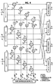
- Each control line 7 j Includes a resistor 8 j and delay elements 9 1j and 9 2j , with the circuit junction between resistor 8 1 and delay element 9 2j being connected to optical gate 4 3j and the junction between delay elements 9 2j and 9 1j being connected to optical gate 4 2j .
- Gate control pulses C j are successively generated at intervals T equal to the duration of the header pulse, and delayed by delay elements 9 2j and 9 1j to successively produce delayed control pulses C ij .
- each of the delay elements 9 introduces a delay time that is one-third of the duration T of the header pulse, and the duration of the triggering voltage of each control pulse is equal to the delay time T/3.
- optical gates 4 3j , 4 2j and 4 1j are supplied with successively shifted control pulses C 3j , C 2j and C 1j , respectively. Therefore, each optical gate of the network of Fig. 4 has a unique triggering instant, and the header pulse of each packet successively coincides with the triggering voltage of a sequence of three control pulses.
- header pulses P1a and P2a should coincide with control pulses C 11 and C 21 , respectively, and header pulse P3a should coincide with control pulse C 32 as seen from Fig. 4. Therefore, header pulses P1a and P2a are inserted to the same interval t 1 -t 4 , and header pulse P3a is inserted to an interval t 4 -t 7 as shown in Fig. 5.
- Fig. 6 is implemented by modifying the embodiment of Fig. 4 in which all delay elements of Fig. 4 are removed from the gate array, directly coupling the voltage-dropping resistors to the associated optical gates. As shown in Fig. 7, this embodiment differs from the Fig.
- each control pulse C j has a duration T
- the header pulse of each optical packet has one-third of the duration T.
- Control pulses C 1 , C 2 , C 3 and C 4 are successively generated at T-intervals.
- control pulse C 1 is delayed so that its triggering high voltage portion successively coincides with headers P1a and P2a (Fig. 2).
- header pulse P1a generates a voltage drop across resistor 8 1
- the voltage at the gate 4 21 is lowered to a level not sufficient to cause it to excite in response to header pulse P2a. Therefore, packet P1 is passed through gate 4 11 , while packet P2 is blocked at gate 4 21 .
- Header pulse P3a is assumed to be assigned a position that coincides with the triggering voltage of control pulse C 2 . Gate 4 32 is thus excited, allowing packet P3 to be routed to combiner 5 2 .
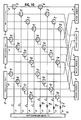
- FIG. 8 A third embodiment of the present invention is shown in Fig. 8. This embodiment differs from the Fig. 1 embodiment by the inclusion of a fourth group of optical gates 4 15 ⁇ 4 18 , a fifth group of optical gates 4 25 ⁇ 4 28 , and a sixth group of optical gates 4 35 ⁇ 4 38 , with the optical gates of the fourth, fifth and sixth groups being respectively connected to the outputs of the optical gates of the first, second and third groups.
- Each of control lines 7 j+4 includes series-connected resistors 10 1j , 10 2j and 10 3j with the junction between resistors 10 1j and 10 2j being connected to optical gates 4 2(j+4) and the junction between resistors 10 2j and 10 3j being connected to optical gates 4 3(j+4) .
- the outputs of optical gates 4 i(j+4) are connected to the i th inputs of combiners 5 j .
- Controller 10c successively applies control pulses C 1a , C 2a , C 3a and C 4a to lines 7 1 ⁇ 7 4 , respectively, during a first interval between times t 1 and t 13 , and successively applies additional control pulses to lines 7 5 ⁇ 7 8 during a second interval between times t 13 and t 25 .
- These additional pulses are indicated by waveforms C 1b , C 2b , C 3b and C 4b in Fig. 9 after experiencing a voltage drop by resistors 10 31 , 10 32 , 10 33 and 10 34 .
- the triggering voltage of each of these control pulses has a duration T and the header pulse of each packet has one-third of the duration T as in the Fig. 7 embodiment.
- the triggering voltage of pulses C 1b , C 2b , C 3b and C 4b on control lines 7 5 ⁇ 7 8 has a voltage level V 1 after experiencing the voltage drop by resistors 10 31 , 10 32 , 10 33 and 10 34 .
- the voltage at the junction of resistors 10 3j and 10 2j drops to a lower level V 2 and the voltage at the junction of resistors 10 2j and 10 1j drops to a lowest level V 3 .
- the optical gate whose triggering voltage is higher than any of the other gates of the same control line is given priority.
- each optical packet has a second header pulse "b" which is spaced from the first header pulse "a" by an interval equal to 4T.
- header pulses P1a and P1b of optical packet P1 are inserted respectively to time slots t 1 ⁇ t 2 and t 13 ⁇ t 14 and the header pulses P2a and P3a of packet P2 occur in the same time slots.
- the header pulses P3a, P3b of packet P3 are assumed to be inserted to positions t 4 ⁇ t 5 and t 16 ⁇ t 17 .
- header pulses P1a and P2a coincide with the triggering voltage of control pulse C 1a
- optical gates 4 11 and 4 21 are simulaneously excited, allowing packets P1 and P2 to be forwarded to optical gates 4 15 and 4 25 , respectively
- header pulse P3a excites gate 4 32 upon coincidence with the triggering voltage of control pulse C 2a , thus applying packet P3 to gate 4 36 .
- Header pulse P1b coincides with the triggering voltage of control pulse C" 1b that is applied to gate 4 15
- header pulse P2b coincides with the triggering voltage of control pulse C' 1b that is applied to gate 4 25 .
- the triggering voltage at gate 4 25 reduces to lower level V 2
- the voltage at gate 4 15 reduces to lowest level V 3 as indicated in Fig. 9, giving priority to gate 4 25 in passing packet P2 to combiner 5 1 .
- Header pulse P3b then coincides with the triggering voltage of control pulse C 2b at gate 4 36 , and packet P3 is passed through it to combiner 5 2 .
- FIG. 10 A modified embodiment of Fig. 8 is shown in Fig. 10 which differs from it by the exclusion of resistors 10 1j and 10 2j from the control lines 7 (j+4) and by the use of second header pulses having different light intensities S 1 , S 2 and S 3 as shown in Fig. 11, with the light intensities having a relationship S 1 > S 2 > S 3 .
- all header pulses of packets P1, P2 and P3 are inserted to the same time slots as in the Fig. 8 embodiment and that their second header pulses P1b, P2b and P3b have light intensities S 1 , S 2 and S 3 , respectively.
- packets P1, P2 and P3 are passed through optical gates and 4 11 , 4 21 and 4 32 , respectively, when their first header pulses P 1a , P 2a , P 3a coincide with control pulses C 1a and C 2a and directed to optical gates 4 15 , 4 25 , and 4 36 , respectively.
- coincidence between header pulse P1a and control pulse C 1b causes gate 4 15 to draw a greater current for excitation than the current drawn by gate 4 25 .
- a sharp voltage drop thus develops across resistor 10 31 , preventing gate 4 25 from being excited.
- packet P1 is given priority over contending packet P2, while packet P3 is allowed to pass through gate 4 36 to combiner 5 2 without contention in response to its second header pulse coinciding with control pulse C 2b .
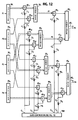
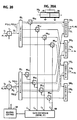
- a fourth embodiment of this invention is shown in Fig. 12 as a 4 x 2 switch configuration.
- Four optical splitters 3 1 ⁇ 3 4 are provided to receive incoming optical packets P1, P2, P3 and P4, respectively.
- optical gates 40 2n have their inputs coupled respectively to the first outputs of splitters 30 3 and 30 4
- optical gates 40 3n have their inputs coupled respectively to the second (lower) outputs of splitters 30 1 and 30 2
- optical gates 40 4n have their inputs coupled respectively to the second outputs of splitters 30 3 and 30 4 .
- Each combiner 50 m has two inputs which are connected to the outputs of the associated optical gates 4 mn .
- the outputs of combiners 50 m are connected respectively to optical gates 41 m .
- the outputs of gates 41 1 and 41 2 are respectively coupled by optical combiner 50 5 to outlet terminal 60 1 , those of gates 41 3 , and 41 4 being coupled by combiner 50 6 to outlet terminal 60 2 .
- Gate controller 10d generates four control pulses C 1 , C 2 , C 3 and C 4 .
- Control pulse C 1 is supplied to gate 40 11 through resistors 11 2 and 11 1 and to gate 40 12 through resistor 11 2 , the same pulse being applied to gate 40 21 through resistors 12 2 and 12 1 and to gate 40 22 through resistor 12 2 , thus supplying different voltages C 11 , C 12 , C 13 and C 14 to gates 40 11 , 40 12 , 40 21 and 40 22 , respectively.
- control pulse C 2 is supplied to gate 40 31 through resistors 13 2 and 13 1 and to gate 40 32 through resistor 13 2 , the same pulse being applied to gate 40 41 through resistors 14 2 and 14 1 and to gate 40 42 through resistor 14 2 , thus supplying different voltages C 21 , C 22 , C 23 and C 24 to gates 40 31 , 40 32 , 40 41 and 40 42 , respectively.
- control pulse C 3 is applied to gate 41 1 through resistors 15 2 and 15 1 and to gate 41 2 through resistor 15 2
- control pulse C 4 is applied to gate 41 3 through resistors 16 2 and 16 1 and to gate 41 2 through resistor 16 2 , thus supplying different voltages C 31, C 32, C 41 and C 42 to gates 41 1 , 41 2 , 41 3 and 41 4 , respectively.
- gates 40 12 , 40 22 , 40 32 , 40 42 , 41 2 and 41 4 are given priority over their companion gates 40 11 , 40 21 , 40 32 , 40 41 , 41 1 and 41 3 , when coincidence occurs between incoming header pulses and their gate control pulses.
- the self-routing network of this configuration can be said to operate on a successive "tournament" basis as will be understood with reference to Fig. 13.
- the triggering voltage of each control pulse has a duration T equal to the duration of each header pulse.
- Timing margins are provided between the leading edges of successive gate control pulses. For purposes of clarity, the timing margins are set equal to the duration T. Assume that a contention is likely to occur between the header pulses P1b and P3b of packets P1 and P3 and between the header pulses P2b and P4b of packets P2 and P4.
- the header pulse P1a of packet P1 coincides with control pulse C 11 at gate 40 11 without contention with gate 40 12 , allowing the packet to be routed through combiner 50 1 to output gate 41 1 , while the header pulse P3a of packet P3 coincides with control pulse C 13 at gate 40 21 without contention with gate 40 22 , routing the packet through combiner 50 2 to output gate 41 2 .
- the header pulse P2a of packet P2 coincides with control pulse C 22 at gate 40 32 without contention with gate 40 31 , allowing the packet to be routed through combiner 50 3 to output gate 41 3
- the header pulse P4a of packet P4 coincides with control pulse C 24 at gate 40 42 without contention with gate 40 41 , routing the packet through combiner 50 4 to output gate 41 4 .
- FIG. 14 An embodiment shown in Fig. 14 is a modification of the embodiment of Fig. 12, the difference being in the exclusion of resistors 11 1 , 12 1 , 13 1 , 14 1 , 15 1 and 16 1 so that equal triggering voltages (C 1a , C 1b , C 2a , C 2b , C 3a , C 4a ) are supplied to the optical gates of contending partners (pairs) and in the generation of header pulses having different light intensities as seen from Fig. 15. As illustrated, the header pulses are assumed to occur in the same time slots as in the case of Fig. 14.
- packets P1 and P3 are routed through input gates without contention to output gates 41 1 and 41 2 between which contention arises, and the other packets are routed to output gates 41 3 and 41 4 between which contention arises.
- the header pulses of packet P1 have the highest light intensity, and those of packets P2, P3 and P4 have decreasing light intensities in the order given. Since header pulses P1b and P2b have a higher light intensity than those of the contending packets, packets routed to output gates 41 1 and 41 3 are the winners of the contentions, so that P1 is passed through combiner 50 5 to outlet terminal 60 1 and P2 is passed through combiner 50 6 to outlet terminal 60 2 .
- a self-routing network of 4 x 2 switch configuration can also be implemented in a single contention stage for each outlet terminal as shown in Fig. 16.
- Optical gates 42 1 ⁇ 42 4 are coupled respectively to the first outputs of splitters 30 1 ⁇ 30 4 for resolving a contention among packets destined to outlet terminal 60 1 through combiner 50 1
- optical gates 43 1 ⁇ 43 4 are coupled respectively to the second outputs of splitters 30 1 ⁇ 30 4 for resolving a contention among packets that are destined to outlet terminal 60 2 through combiner 50 2 .
- Gate controller 10e supplies a control pulse C 1 through series-connected resistors 17 4 , 17 3 , 17 2 and 17 1 to develop successively decreasing control voltages C 14 , C 13 , C 12 and C 11 for coupling to gates 42 4 , 42 3 , 42 2 and 42 1 , respectively.
- gate controller 10e further supplies a control pulse C 2 through series-connected resistors 18 4 , 18 3 , 18 2 and 18 1 to develop successively decreasing control voltages C 24 , C 23 , C 22 and C 21 for coupling to gates 43 4 , 43 3 , 43 2 and 43 1 , respectively.
- each optical packet has a single header pulse. If header pulse P1a and P3a occur in the same time slot t 1 -t 2 so that packets P1 and P3 are destined to outlet terminal 60 1 , and header pulse P2a and P4a occur in the same time slot t 2 -t 3 so that packets P2 and P4 are destined to outlet terminal 60 2 , contention occurs at gates 42 1 and 42 3 as well as at gates 43 2 and 43 4 as packets P1 and P3 coincide with control pulses C 11 and C 13 , respectively, and th other packets P2 and P4 coincide with control pulses C 22 and C 24 , respectively.
- gate 42 3 Since gate 42 3 is supplied with a higher triggering voltage than the voltage supplied to gate 42 1 , packet P3 wins the race for contention with packet P1.
- gate 43 4 is supplied with a higher triggering voltage than the voltage at gate 43 1 , packet P4 is the winner.
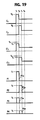
- Fig. 18 is a modification of the embodiment of Fig. 16, the difference being in the exclusion of resistors 17 1 ⁇ 17 3 and resistors 18 1 ⁇ 18 3 so that equal triggering voltages (C' 1 and C' 2 ) are supplied to the optical gates of contending partners (sets) and in the generation of header pulses having different light intensities as seen from Fig. 19.
- the header pulses are assumed to occur in the same time slots as in the case of Fig. 17.
- packets P1 and P3 are applied to gates 42 1 and 42 3 , respectively, and packets P2 and P4 are applied to gates 43 2 and 43 4 , respectively.
- packets P1 and P3 are applied to gates 42 1 and 42 3 , respectively
- packets P2 and P4 are applied to gates 43 2 and 43 4 , respectively.
- header pulses of packet P1 have the highest light intensity, and those of packets P2, P3 and P4 have decreasing light intensities in the order given. Since header pulses P1b and P2b have a higher light intensity than those of the contending packets, packets P1 and P2 supplied to gates 42 1 and 43 2 are the winners of the race to respective outlet terminals 60 1 and 60 2 .
- the length of a header increases with the amount of traffic to be carried by the self-routing network.
- the header length can be conserved by multiplexing optical packets upon different light wavelengths.
- the wavelength multiplexing concept of this invention for two wavelengths is implemented by a 2 x 4 network configuration as shown In Fig. 20. Electrical packets P1 and P2 from a user station are successively transmitted on access line L 1 and received by line interface 1' 1 and packets P3 and P4 from another user station are successively transmitted on access line L 2 and received by line interface 1' 2 .
- Routing controller 120 is coupled to the line interfaces, determines a wavelength and a header time slot according to the information contained in a packet received from the associated interface in relation to the timing and amplitude pattern of the gate control pulses supplied from gate controller 10f, and instructs the interface to carry the packet on the determined wavelength and insert a header pulse Into the determined time slot.
- packets P1 and P2 are converted by line interface 1' 1 to optical signals of wavelength ⁇ 1
- packets P3 and P4 are converted by line interface l' 2 to optical signals of wavelengths ⁇ 2 and ⁇ 1 , respectively.
- interfaces 1' 1 and 1' 2 are connected respectively by light waveguides 70 1 and 70 2 to optical splitters 80 1 and 80 2 , each having four outputs.
- Optical gates 90 11 , 90 12 , 90 13 and 90 14 are connected respectively to the outputs of splitter 80 1 , and gates 90 11 and 90 12 are tuned to wavelength ⁇ 1 , and gates 90 13 and 90 14 are tuned to wavelength ⁇ 2 .
- Optical gates 90 21 , 90 22 , 90 23 and 90 24 are likewise connected to the outputs of splitter 80 2 , with gates 90 21 and 90 22 being tuned to wavelength ⁇ 1 and gates 90 23 and 90 24 being tuned to wavelength ⁇ 2 .
- each of the optical gates 90 ij is preferably constructed of a narrow-band wavelength tunable optical element 85 and a wide-band wavelength tunable optical element 86 coupled together and arranged in the path of incident light beam.
- control pulses C 1 ⁇ C 4 have equal amplitude V H for gate excitation, with the triggering voltages of pulses C 1 and C 3 having an equal time slot t 1 -t 2 and those of pulses C 2 and C 4 having an equal time slot t 2 -t 3 .
- control pulses C 1 and C 2 have a trailing voltage V L1 for tuning to wavelength ⁇ 1
- the trailing voltage of pulses C 3 and C 4 is set equal to V L2 for tuning to wavelength ⁇ 2 .
- header pulses P1a and P2a for packets P1( ⁇ 1 ) and P2( ⁇ 1 ) are inserted into the same time slot t 1 -t 2 of successive headers and the header pulse P3a of packet P3( ⁇ 2 ) is inserted to the time slot t 1 -t 2 of an initial header.
- the header pulse P4a of packet P4( ⁇ 1 ) is assumed to be inserted to the time slot t 2 -t 3 of a subsequent header.
- header pulses P1a and P2a successively coincide with control pulse C 1 at gate 90 11 , so packets P1( ⁇ 1 ) and P2( ⁇ 1 ) are routed to on outlet terminal 110 1 via combiner 100 1 .
- Header pulse P3a coincides with control pulse C 3 at gate 90 23 , allowing packet P3( ⁇ 2 ) to be routed to outlet terminal 110 3 via combiner 100 3 .
- header pulse P4a coincides with control pulse C 2 at gate 90 22 , routing packet P4( ⁇ 1 ) to outlet terminal 110 2 via combiner 100 2 .
- Fig. 20 is modified as shown in Fig. 22 in which the network is implemented in a 4 x 2 switch configuration.
- Gates 91 i1 and 91 i2 are tuned to wavelength ⁇ 1 and ⁇ 2 , respectively, and supplied with control pulses C' 1 and C' 2 via resistors 19 1 and 19 2 , respectively, from gate controller 10g.
- gate control pulses C 1 and C 2 generated by controller 10g have triggering voltages of a duration twice as long as the duration of the header pulse. Assume that header pulses P1a and P2a are inserted to time slot t 1 -t 2 , and header pulses P3a and P4a are assigned time slot t 2 -t 3 . It is seen that gate 91 11 is excited upon coincidence between header pulse P1a and control pulse C' 1 , producing a voltage drop across resistor 19 1 and allowing packet P1( ⁇ 1 ) to be routed to combiner 100 1 .
- gate 91 22 is excited upon coincidence between header pulse P2a and control pulse C' 2 , producing a voltage drop across resistor 19 2 and allowing packet P2( ⁇ 2 ) to be routed to combiner 100 2 .
- gate 91 31 is not excited and packet P3( ⁇ 1 ) is the loser of the contention with packet P1( ⁇ 1 ).
- packet P4( ⁇ 2 ) is the loser of the contention with packet P2( ⁇ 2 ).
- the triggering voltages of all control pulses are of equal duration to the duration of the header pulse and the header of each packet has different light intensities as shown in Fig. 23B.
- packets P1 ⁇ P4 have decreasing levels of priority in the order named so that contention between packets P1 and P3 at gates 91 11 and 91 31 is resolved by giving priority to packet P1, while contention between packets P2 and P4 Is resolved by giving priority to packet P2.
Landscapes
- Engineering & Computer Science (AREA)
- Computer Networks & Wireless Communication (AREA)
- Data Exchanges In Wide-Area Networks (AREA)
- Optical Communication System (AREA)
- Use Of Switch Circuits For Exchanges And Methods Of Control Of Multiplex Exchanges (AREA)
Claims (13)
- Selbstleitweglenkendes optisches Netzwerk, das aufweist:N optische Verteiler (31-33), die N Eingangsanschlüssen (21-23) zugeordnet sind, wobei jeder der Verteiler ein optisches Signal vom zugeordneten Eingangsanschluß in M Kopien des optischen Signals aufspaltet;M optische Kombinatoren (51-54), die M Ausgangsanschlüssen (61-64) zugeordnet sind, wobei jeder der optischen Kombinatoren N dort einfallende optische Signale zu einem kombinierten optischen Signal vereinigt und das kombinierte optische Signal an den zugeordneten Ausgangsanschluß ankoppelt;N x M optische Gatter (4), die zwischen die N optischen Verteiler (3) und die M optischen Kombinatoren (5) geschaltet sind, wobei jedes der optischen Gatter ein dort einfallendes optisches Signal durchläßt, wenn das einfallende optische Signal mit einem dort anliegenden elektrischen Signal zeitlich zusammenfällt, wobei die optischen Gatter (4) in M Sätze von N optischen Gattern unterteilt sind;eine Gattersteuereinrichtung (10) zum Zuführen eines elektrischen Gattersteuersignals zu den optischen Gattern (4) jedes Satzes; dadurch gekennzeichnet, daßdie Gattersteuereinrichtung (10) so eingerichtet ist, daß sie während M aufeinanderfolgender Intervalle elektrische Gattersteuersignale (Cn, Cij) den optischen Gattern jedes Satzes jeweils so zuführt, daß eines der optischen Gatter eines gegebenen Satzes nur dann ein dort einfallendes optisches Signal (Pn, Pij) durchläßt, wenn das dort anliegende elektrische Gattersteuersignal von den elektrischen Gattersteuersignalen, die nacheinander an die optischen Gatter des gegebenen Satzes angelegt werden, das früheste Signal ist oder die höchste Amplitude aufweist, oder wenn das einfallende optische Signal das früheste von den in die optischen Gatter des Satzes einfallenden Signalen ist oder die höchste Intensität aufweist.
- Selbstleitweglenkendes Netzwerk nach Anspruch 1, dadurch gekennzeichnet, daß die an den optischen Gattern jedes Satzes anliegenden elektrischen Gattersteuersignale (C3i-C1i) stufenweise zeitlich verschoben sind.
- Selbstleitweglenkendes optisches Netzwerk nach Anspruch 1, dadurch gekennzeichnet, daß die optischen Gatter jedes Satzes gemeinsam einem einzigen Zeitintervall (t1-t4) zugeordnet sind, und daß die den optischen Gattern jedes Satzes zugeführten optischen Signale (P1a-P3a) stufenweise verschoben sind.
- Selbstleitweglenkendes optisches Netzwerk nach Anspruch 1, dadurch gekennzeichnet, daß die den optischen Gattern jedes Satzes zugeführten elektrischen Gattersteuersignale verschiedene Amplituden (V1-V3) aufweisen.
- Selbstleitweglenkendes optisches Netzwerk nach Anspruch 1, dadurch gekennzeichnet, daß die an die optischen Gatter jedes Satzes angelegten optischen Signale verschiedene Intensitäten (S1-S3) aufweisen.
- Selbstleitweglenkendes optisches Netzwerk nach Anspruch 1, dadurch gekennzeichnet, daß das optische Signal ein Paket mit einem ersten und einem zweiten Kopf ist;daß die optischen Gatter in eine erste Matrix von M Sätzen mit jeweils N optischen Gattern (411, 421, 431; 412, 422, 432; 413, 423, 433; 414, 424, 434; Fig. 8) und eine zweite Matrix von M Sätzen mit jeweils N optischen Gattern (415, 425, 435; 416, 426, 436; 417, 427, 437; 418, 428, 438) unterteilt sind;daß die N optischen Gatter jedes Satzes der ersten Matrix jeweils an ihren Eingangsenden mit den N optischen Verteilern (31-33) verbunden sind, wobei jedes optische Gatter jedes Satzes der ersten Matrix eine von M Kopien eines vom entsprechenden optischen Verteiler einfallenden optischen Pakets empfängt und bei einem zeitlichen Zusammenfallen zwischen dem ersten Kopf der einfallenden Kopie und einem ersten elektrischen Steuersignal die einfallende Kopie durchläßt;daß die M Sätze der zweiten Matrix jeweils den M optischen Kombinatoren (51-54) entsprechen und die N optischen Gatter jedes Satzes der zweiten Matrix an ihren Eingangsenden jeweils mit den N optischen Gattern jedes Satzes der ersten Matrix und an ihren Ausgangsenden mit dem optischen Kombinator verbunden sind, dem der Satz der optischen Gatter entspricht, wobei jedes optische Gatter der zweiten Matrix ein von der ersten Matrix einfallendes optisches Paket empfängt und das einfallende optische Paket durchläßt, wenn der zweite Kopf des einfallenden Pakets mit einem zweiten elektrischen Steuersignal zeitlich zusammenfällt; unddaß die Gattersteuereinrichtung (10c) jedem Satz von optischen Gattern der ersten Matrix während M aufeinanderfolgender Intervalle ein elektrisches Gattersteuersignal als erstes elektrisches Steuersignal zuführt, anschließend während M aufeinanderfolgender Intervalle den optischen Gattern jedes Satzes der zweiten Matrix jeweils gleichzeitig N elektrische Gattersteuersignale mit verschiedenen Amplituden als zweites elektrisches Steuersignal zuführt, so daß eines der N optischen Gatter eines gegebenen Satzes der zweiten Matrix nur dann ein dort einfallendes optisches Paket durchläßt, wenn die Amplitude des dort anliegenden elektrischen Gattersteuersignals die höchste Amplitude der elektrischen Gattersteuersignale ist, die an den N optischen Gattern des gegebenen Satzes anliegen.
- Selbstleitweglenkendes optisches Netzwerk nach Anspruch 1, dadurch gekennzeichnet, daß das optische Signal ein Paket mit einem ersten und einem zweiten Kopf ist;daß die optischen Gatter in eine erste Matrix von M Sätzen mit jeweils N optischen Gattern (411, 421, 431; 412, 422, 432; 413, 423, 433; 414, 424, 434; Fig. 10) und eine zweite Matrix von M Sätzen mit jeweils N optischen Gattern (415, 425, 435, 416, 426, 436, 417, 427, 437; 418, 428, 438) unterteilt sind;daß die N optischen Gatter jedes Satzes der ersten Matrix an ihren Eingangsenden jeweils mit den N optischen Verteilern (31-33) verbunden sind, wobei jedes optische Gatter jedes Satzes eine von M Kopien eines vom entsprechenden optischen Verteiler einfallenden optischen Pakets empfängt und die einfallende Kopie durchläßt, wenn der erste Kopf der einfallenden Kopie mit einem ersten elektrischen Steuersignal zeitlich zusammenfällt;daß die M Sätze der zweiten Matrix jeweils den M optischen Kombinatoren (51-54) entsprechen, und daß die N optischen Gatter jedes Satzes der zweiten Matrix jeweils an ihren Eingangsenden mit den N optischen Gattern jedes Satzes der ersten Matrix und an ihren Ausgangsenden mit dem optischen Kombinator verbunden sind, dem der Satz von optischen Gattern entspricht, wobei jedes optische Gatter der zweiten Matrix ein von der ersten Matrix einfallendes optisches Paket empfängt und das einfallende optische Paket durchläßt, wenn der zweite Kopf des einfallenden Pakets mit einem zweiten elektrischen Steuersignal zeitlich zusammenfällt;daß die optischen Gatter jeder Matrix einem einzigen Zeitintervall zugeordnet sind und die ersten Köpfe von optischen Paketen, die in die optischen Gatter der ersten Matrix einfallen, zu verschiedenen Zeitpunkten innerhalb des einzigen Zeitintervalls auftreten, und daß die zweiten Köpfe von optischen Paketen, die in die optischen Gatter der zweiten Matrix einfallen, verschiedene Lichtintensitäten aufweisen; unddaß die Gattersteuereinrichtung (10c) während M aufeinanderfolgender Intervalle jedem Satz von optischen Gattern der ersten Matrix ein elektrisches Gattersteuersignal als erstes elektrisches Steuersignal zuführt, anschließend während M aufeinanderfolgender Intervalle jedem Satz von optischen Gattern der zweiten Matrix ein elektrisches Gattersteuersignal als zweites elektrisches Steuersignal zuführt, so daß eines der N optischen Gatter eines gegebenen Satzes der zweiten Matrix ein dort einfallendes optisches Paket nur dann durchläßt, wenn die Lichtintensität des zweiten Kopfes des einfallenden optischen Pakets die höchste Lichtintensität der zweiten Köpfe der optischen Pakete ist, die in die N optischen Gatter des gegebenen Satzes einfallen.
- Selbstleitweglenkendes optisches Netzwerk nach Anspruch 1, dadurch gekennzeichnet, daß das optische Signal ein Paket mit einem ersten und einem zweiten Kopf ist;daß die optischen Gatter (4011-4042, 411-414) in mehrere Paare von optischen Gattern (4011-4042) einer ersten Stufe und mehrere Paare von optischen Gattern (411-414) einer zweiten Stufe unterteilt sind, und daß die optischen Kombinatoren in mehrere optische Kombinatoren (501-504) einer ersten Stufe und mehrere optische Kombinatoren (505-506) einer zweiten Stufe unterteilt sind, wobei die optischen Kombinatoren der ersten Stufe jeweils den Paaren von optischen Gattern der ersten Stufe und die optischen Kombinatoren der zweiten Stufe jeweils den Paaren von optischen Gattern der zweiten Stufe zugeordnet sind;daß jedes der optischen Gatter (4011-4042) der ersten Stufe ein einfallendes optisches Paket zum zugehörigen Kombinator (50) der ersten Stufe durchläßt, wenn der erste Kopf des einfallenden optischen Pakets mit einem dort anliegenden ersten elektrischen Steuersignal zeitlich zusammenfällt;daß jedes der optischen Gatter (411-414) der zweiten Stufe ein dort einfallendes optisches Paket von dem zugehörigen Kombinator (501-505) der ersten Stufe empfängt und das einfallende optische Paket zum zugehörigen Kombinator (505-506) der zweiten Stufe durchläßt, wenn der zweite Kopf des einfallenden optischen Pakets mit einem dort anliegenden zweiten elektrischen Steuersignal zeitlich zusammenfällt; unddaß die Gattersteuereinrichtung (10d) den optischen Gattern jedes Paares der ersten Stufe jeweils gleichzeitig elektrische Gattersteuersignale mit verschiedenen Amplituden als erstes elektrisches Steuersignal zuführt, so daß eines der optischen Gatter eines gegebenen Paares der ersten Stufe ein dort einfallendes optisches Paket nur dann durchläßt, wenn die Amplitude des dort anliegenden elektrischen Gattersteuersignals die höchste Amplitude der Signale ist, die an den optischen Gattern des gegebenen Paares anliegen, und anschließend den optischen Gattern der zweiten Stufe jeweils gleichzeitig elektrische Gattersteuersignale mit verschiedenen Amplituden als zweites elektrisches Steuersignal zuführt, so daß eines der optischen Gatter der zweiten Stufe ein dort einfallendes optisches Paket nur dann durchläßt, wenn die Amplitude des dort anliegenden elektrischen Gattersteuersignals die höchste Amplitude der Signale ist, die an den optischen Gattern der zweiten Stufe anliegen.
- Selbstleitweglenkendes optisches Netzwerk nach Anspruch 1, dadurch gekennzeichnet, daß das optische Signal ein Paket mit einem ersten und einem zweiten Kopf ist;daß die optischen Gatter (4011-4042, 411-414) in mehrere Paare von optischen Gattern einer ersten Stufe (4011-4042) und mehrere Paare von optischen Gattern einer zweiten Stufe (411-414) unterteilt sind, und daß die optischen Kombinatoren in mehrere optische Kombinatoren einer ersten Stufe (501-504) und mehrere optische Kombinatoren einer zweiten Stufe (505-506) unterteilt sind, wobei die optischen Kombinatoren der ersten Stufe jeweils den Paaren von optischen Gattern der ersten Stufe und die optischen Kombinatoren der zweiten Stufe jeweils den Paaren von optischen Gattern der zweiten Stufe zugeordnet sind;daß jedes der optischen Gatter der ersten Stufe (4011-4042) ein einfallendes optisches Paket zu dem zugehörigen Kombinator der ersten Stufe (50) durchläßt, wenn der erste Kopf des einfallenden optischen Pakets mit einem dort anliegenden ersten elektrischen Steuersignal zeitlich zusammenfällt;daß jedes der optischen Gatter der zweiten Stufe (411-414) ein dort einfallendes optisches Paket vom zugehörigen Kombinator der ersten Stufe (501-505) empfängt und das einfallende optische Paket zum zugehörigen Kombinator der zweiten Stufe (505, 506) durchläßt, wenn der zweite Kopf des einfallenden optischen Pakets mit einem dort anliegenden zweiten elektrischen Steuersignal zeitlich zusammenfällt; unddaß die Gattersteuereinrichtung (10d, Fig. 14, 15) den optischen Gattern der ersten Stufe gleichzeitig ein elektrisches Gattersteuersignal als erstes elektrisches Steuersignal zuführt, so daß eines der optischen Gatter eines gegebenen Paares der ersten Stufe ein dort einfallendes optisches Paket nur dann durchläßt, wenn die Lichtintensität des ersten Kopfes des einfallenden optischen Pakets die höchste Lichtintensität der ersten Köpfe ist, die in die optischen Gatter des gegebenen Paares einfallen, und anschließend den optischen Gattern der zweiten Stufe gleichzeitig ein elektrisches Gattersteuersignal als zweites elektrisches Steuersignal zuführt, so daß eines der optischen Gatter der zweiten Stufe ein dort einfallendes optisches Paket nur dann durchläßt, wenn die Lichtintensität des zweiten Kopfes des einfallenden optischen Pakets die höchste Lichtintensität der zweiten Köpfe ist, die in die optischen Gatter der zweiten Stufe einfallen.
- Selbstleitweglenkendes optisches Netzwerk nach einem der Ansprüche 8 oder 9, dadurch gekennzeichnet, daß die Anzahl der optischen Kombinatoren der ersten Stufe (501-504) gleich der halben Anzahl der optischen Gatter der ersten Stufe (4011-4042) ist, daß die Anzahl der optischen Gatter der zweiten Stufe (411-414) gleich der Anzahl der optischen Kombinatoren der ersten Stufe (501-504) ist, und daß die Anzahl der optischen Kombinatoren der zweiten Stufe (505-506) gleich einem Viertel der Anzahl der optischen Gatter der ersten Stufe (4011-4042) ist.
- Selbstleitweglenkendes optisches Netzwerk nach einem der Ansprüche 1, 4 oder 5, dadurch gekennzeichnet, daß die an das selbstleitweglenkende Netzwerk angelegten optischen Signale auf mehreren Trägerwellenlängen übertragen werden und daß jedes der optischen Gatter für ein optisches Signal mit einer der Wellenlängen selektiv durchlässig ist.
- Selbstleitweglenkendes optisches Netzwerk nach Anspruch 11, dadurch gekennzeichnet, daß jedes der optischen Gatter (9011-9014, 9021-9024) ein optisches Schmalband-Gatterelement (85) zum Durchlassen eines optischen Pakets, das von einer Seite des optischen Gatters einfällt, sowie ein mit dem optischen Schmalband-Gatter verbundenes optisches Breitband-Gatterelement (86) aufweist, um ein von dem optischen Schmalband-Gatterelement einfallendes optisches Paket zur anderen Seite des optischen Gatters durchzulassen.
- Selbstleitweglenkendes optisches Netzwerk nach Anspruch 1, das ferner Einrichtungen (30, 32, Fig. 3) aufweist, die zwischen den N optischen Verteilern und den N x M optischen Gattern angeordnet sind, um optische Signale von den Verteilern zu den N x M optischen Gattern durchzulassen und von den optischen Gattern zurückkehrende optische Signale zu den M optischen Kombinatoren zu lenken.
Applications Claiming Priority (8)
| Application Number | Priority Date | Filing Date | Title |
|---|---|---|---|
| JP307649/90 | 1990-11-14 | ||
| JP2307649A JP2827501B2 (ja) | 1990-11-14 | 1990-11-14 | 光セルフ・ルーテイング回路 |
| JP3597091A JP2850550B2 (ja) | 1991-03-01 | 1991-03-01 | 光セルフルーティング回路 |
| JP35970/91 | 1991-03-01 | ||
| JP8588091A JP2855878B2 (ja) | 1991-03-27 | 1991-03-27 | 光セルフルーティング回路 |
| JP85880/91 | 1991-03-27 | ||
| JP178234/91 | 1991-07-18 | ||
| JP17823491A JP2748726B2 (ja) | 1991-07-18 | 1991-07-18 | 光セルフルーティング回路 |
Publications (3)
| Publication Number | Publication Date |
|---|---|
| EP0486023A2 EP0486023A2 (de) | 1992-05-20 |
| EP0486023A3 EP0486023A3 (en) | 1993-05-12 |
| EP0486023B1 true EP0486023B1 (de) | 1997-08-27 |
Family
ID=27460184
Family Applications (1)
| Application Number | Title | Priority Date | Filing Date |
|---|---|---|---|
| EP91119452A Expired - Lifetime EP0486023B1 (de) | 1990-11-14 | 1991-11-14 | Selbstleitweglenkendes Netzwerk mit optischer Gattermatrix |
Country Status (4)
| Country | Link |
|---|---|
| US (1) | US5341234A (de) |
| EP (1) | EP0486023B1 (de) |
| CA (1) | CA2055546C (de) |
| DE (1) | DE69127423T2 (de) |
Families Citing this family (15)
| Publication number | Priority date | Publication date | Assignee | Title |
|---|---|---|---|---|
| US5617413A (en) * | 1993-08-18 | 1997-04-01 | The United States Of America As Represented By The Administrator Of The National Aeronautics And Space Administration | Scalable wrap-around shuffle exchange network with deflection routing |
| NZ313707A (en) * | 1995-07-28 | 1999-04-29 | British Telecomm | Packet routing comprising a packet, node and directional flag |
| FR2754352B1 (fr) * | 1996-10-07 | 1998-11-13 | Alsthom Cge Alcatel | Commutateur optique |
| US6271949B1 (en) * | 1996-12-18 | 2001-08-07 | Nec Corporation | Optical communication system using wavelength-division multiplexed light |
| US5959767A (en) * | 1996-12-31 | 1999-09-28 | Lucent Technologies | Loss-less optical cross-connect |
| JP3481442B2 (ja) | 1997-12-22 | 2003-12-22 | 日本電気株式会社 | 光ネットワーク |
| US6128113A (en) * | 1998-03-04 | 2000-10-03 | Dynamics Research Corporation | Transparent optical communications switch |
| JPH11275614A (ja) * | 1998-03-26 | 1999-10-08 | Nec Corp | 光交換装置 |
| KR100295097B1 (ko) | 1998-08-22 | 2001-08-07 | 오길록 | 광게이트를이용한광공간분할스위칭장치 |
| US6782210B1 (en) * | 1999-08-25 | 2004-08-24 | Nippon Telegraph And Telephone Corporation | Optical packet routing network system based on optical label switching technique |
| JP4290320B2 (ja) * | 2000-09-28 | 2009-07-01 | 富士通株式会社 | ルーチング装置 |
| US20020122225A1 (en) * | 2001-03-01 | 2002-09-05 | Yigal Rappaport | Multiport wavelength division multiplex network element |
| US6501886B1 (en) * | 2001-07-30 | 2002-12-31 | Agilent Technologies, Inc. | Compact optical splitter and combiner |
| US7161936B1 (en) * | 2001-12-28 | 2007-01-09 | Cisco Technology, Inc. | Method and system for distributing data communications utilizing a crossbar switch |
| US9729946B2 (en) * | 2009-04-03 | 2017-08-08 | Infinera Corporation | High-capacity switch |
Family Cites Families (14)
| Publication number | Priority date | Publication date | Assignee | Title |
|---|---|---|---|---|
| GB945373A (en) * | 1960-09-02 | 1963-12-23 | Ass Elect Ind | Improvements relating to static switching arrangements of the cross-point type |
| GB945374A (en) * | 1960-11-04 | 1963-12-23 | Ass Elect Ind | Improvements relating to switching systems employing co-ordinate switching arrangements of the cross-point type |
| US3141067A (en) * | 1960-11-17 | 1964-07-14 | Lester M Spandorfer | Automatic electronic communication switching exchange |
| US3223978A (en) * | 1962-06-08 | 1965-12-14 | Radiation Inc | End marking switch matrix utilizing negative impedance crosspoints |
| US3452157A (en) * | 1966-02-01 | 1969-06-24 | Itt | Current controlled,self-seeking telephone switching system |
| US4731878A (en) * | 1985-11-29 | 1988-03-15 | American Telephone And Telegraph Company, At&T Bell Laboratories | Self-routing switch node combining electronic and photonic switching |
| US4787692A (en) * | 1987-03-13 | 1988-11-29 | American Telephone And Telegraph Company At&T Bell Laboratories | Electro optical switch architectures |
| CA1331800C (en) * | 1987-09-30 | 1994-08-30 | Syuji Suzuki | Time and wavelength division switching system |
| JPH0834479B2 (ja) * | 1987-10-22 | 1996-03-29 | 国際電信電話株式会社 | 光パケット交換方式 |
| IT1219054B (it) * | 1988-02-29 | 1990-04-24 | Cselt Centro Studi Lab Telecom | Nodo per rete a commutazione veloce di pacchetto in tecnologia ottico elettrica |
| JPH025663A (ja) * | 1988-06-23 | 1990-01-10 | Nec Corp | 光パケット交換装置 |
| US5023864A (en) * | 1989-05-08 | 1991-06-11 | At&T Bell Laboratories | Crossover network utilizing two-dimensional arrays of nodes |
| JP2692316B2 (ja) * | 1989-11-20 | 1997-12-17 | 日本電気株式会社 | 波長分割光交換機 |
| US5181134A (en) * | 1991-03-15 | 1993-01-19 | At&T Bell Laboratories | Photonic cross-connect switch |
-
1991
- 1991-11-14 EP EP91119452A patent/EP0486023B1/de not_active Expired - Lifetime
- 1991-11-14 US US07/792,191 patent/US5341234A/en not_active Expired - Fee Related
- 1991-11-14 CA CA002055546A patent/CA2055546C/en not_active Expired - Fee Related
- 1991-11-14 DE DE69127423T patent/DE69127423T2/de not_active Expired - Fee Related
Also Published As
| Publication number | Publication date |
|---|---|
| US5341234A (en) | 1994-08-23 |
| DE69127423T2 (de) | 1998-02-19 |
| DE69127423D1 (de) | 1997-10-02 |
| CA2055546C (en) | 1999-02-02 |
| CA2055546A1 (en) | 1992-05-15 |
| EP0486023A3 (en) | 1993-05-12 |
| EP0486023A2 (de) | 1992-05-20 |
Similar Documents
| Publication | Publication Date | Title |
|---|---|---|
| US5739933A (en) | Optically controlled optical switching module, method of optically controlling an optical switching network, and optical switching network | |
| US5341234A (en) | Self-routing network using optical gate array driven by control voltages coincidental with packet header pulses | |
| Chlamtac et al. | CORD: Contention resolution by delay lines | |
| CA2061919C (en) | Optical switch and switching module therefor | |
| US5319486A (en) | Transmission equipment with an optical transmission line | |
| US5912753A (en) | Optical telecommunications network | |
| JP2953894B2 (ja) | 光パケット交換機 | |
| US5539559A (en) | Apparatus and method for photonic contention resolution in a large ATM switch | |
| EP0236796A2 (de) | Optisches Schaltsystem | |
| US5365344A (en) | System for transmitting data using wavelength division multiplexing | |
| US5521732A (en) | Optical wavelength selection control system in optical networks | |
| JPH07212347A (ja) | 波長多重光通信システム | |
| EP0189273A2 (de) | Lichtwellenleiternetzwerk mit verminderten Kopplungsverlusten | |
| EP0781006A2 (de) | Ringnetz mit Wellenlängenmultiplexing | |
| EP0658992A1 (de) | Optisches Übertragungssystem | |
| US4896934A (en) | Broadband optical multicast switch | |
| JPH07202847A (ja) | 複数のアクセスが可能な波長分割多重化パケットネットワーク | |
| US5828669A (en) | Network system connecting node devices with plural channels, node device used therein, and transmission control method therefor | |
| US5485298A (en) | Optical packet synchronization circuit | |
| RU2121230C1 (ru) | Оптическое устройство коммутации для проключения оптических ячеек информации | |
| CA1287911C (en) | Multichannel, multihop lightwave communication network | |
| JPH11344638A (ja) | 光ネットワ―クのためのリング・カプラ | |
| JP3589537B2 (ja) | 光バッファメモリ装置 | |
| AU762271B2 (en) | Optical device for processing a sequence of bits | |
| JP2855878B2 (ja) | 光セルフルーティング回路 |
Legal Events
| Date | Code | Title | Description |
|---|---|---|---|
| PUAI | Public reference made under article 153(3) epc to a published international application that has entered the european phase |
Free format text: ORIGINAL CODE: 0009012 |
|
| 17P | Request for examination filed |
Effective date: 19911211 |
|
| AK | Designated contracting states |
Kind code of ref document: A2 Designated state(s): DE FR GB NL |
|
| PUAL | Search report despatched |
Free format text: ORIGINAL CODE: 0009013 |
|
| AK | Designated contracting states |
Kind code of ref document: A3 Designated state(s): DE FR GB NL |
|
| 17Q | First examination report despatched |
Effective date: 19940406 |
|
| GRAG | Despatch of communication of intention to grant |
Free format text: ORIGINAL CODE: EPIDOS AGRA |
|
| GRAH | Despatch of communication of intention to grant a patent |
Free format text: ORIGINAL CODE: EPIDOS IGRA |
|
| GRAH | Despatch of communication of intention to grant a patent |
Free format text: ORIGINAL CODE: EPIDOS IGRA |
|
| GRAA | (expected) grant |
Free format text: ORIGINAL CODE: 0009210 |
|
| AK | Designated contracting states |
Kind code of ref document: B1 Designated state(s): DE FR GB NL |
|
| REF | Corresponds to: |
Ref document number: 69127423 Country of ref document: DE Date of ref document: 19971002 |
|
| ET | Fr: translation filed | ||
| PLBE | No opposition filed within time limit |
Free format text: ORIGINAL CODE: 0009261 |
|
| STAA | Information on the status of an ep patent application or granted ep patent |
Free format text: STATUS: NO OPPOSITION FILED WITHIN TIME LIMIT |
|
| 26N | No opposition filed | ||
| PGFP | Annual fee paid to national office [announced via postgrant information from national office to epo] |
Ref country code: GB Payment date: 19981120 Year of fee payment: 8 |
|
| PGFP | Annual fee paid to national office [announced via postgrant information from national office to epo] |
Ref country code: FR Payment date: 19981127 Year of fee payment: 8 |
|
| PGFP | Annual fee paid to national office [announced via postgrant information from national office to epo] |
Ref country code: NL Payment date: 19981130 Year of fee payment: 8 |
|
| PGFP | Annual fee paid to national office [announced via postgrant information from national office to epo] |
Ref country code: DE Payment date: 19990129 Year of fee payment: 8 |
|
| PG25 | Lapsed in a contracting state [announced via postgrant information from national office to epo] |
Ref country code: GB Free format text: LAPSE BECAUSE OF NON-PAYMENT OF DUE FEES Effective date: 19991114 |
|
| PG25 | Lapsed in a contracting state [announced via postgrant information from national office to epo] |
Ref country code: NL Free format text: LAPSE BECAUSE OF NON-PAYMENT OF DUE FEES Effective date: 20000601 |
|
| GBPC | Gb: european patent ceased through non-payment of renewal fee |
Effective date: 19991114 |
|
| PG25 | Lapsed in a contracting state [announced via postgrant information from national office to epo] |
Ref country code: FR Free format text: LAPSE BECAUSE OF NON-PAYMENT OF DUE FEES Effective date: 20000731 |
|
| NLV4 | Nl: lapsed or anulled due to non-payment of the annual fee |
Effective date: 20000601 |
|
| PG25 | Lapsed in a contracting state [announced via postgrant information from national office to epo] |
Ref country code: DE Free format text: LAPSE BECAUSE OF NON-PAYMENT OF DUE FEES Effective date: 20000901 |
|
| REG | Reference to a national code |
Ref country code: FR Ref legal event code: ST |