EP0486062A1 - Oscillateur haute fréquence - Google Patents
Oscillateur haute fréquence Download PDFInfo
- Publication number
- EP0486062A1 EP0486062A1 EP91119562A EP91119562A EP0486062A1 EP 0486062 A1 EP0486062 A1 EP 0486062A1 EP 91119562 A EP91119562 A EP 91119562A EP 91119562 A EP91119562 A EP 91119562A EP 0486062 A1 EP0486062 A1 EP 0486062A1
- Authority
- EP
- European Patent Office
- Prior art keywords
- change
- mesfet
- gate
- effect transistor
- gate voltage
- Prior art date
- Legal status (The legal status is an assumption and is not a legal conclusion. Google has not performed a legal analysis and makes no representation as to the accuracy of the status listed.)
- Granted
Links
- 229910001218 Gallium arsenide Inorganic materials 0.000 claims abstract description 12
- 230000005669 field effect Effects 0.000 claims description 8
- 239000004065 semiconductor Substances 0.000 claims description 3
- 230000004888 barrier function Effects 0.000 claims 3
- 230000005540 biological transmission Effects 0.000 abstract description 2
- JBRZTFJDHDCESZ-UHFFFAOYSA-N AsGa Chemical compound [As]#[Ga] JBRZTFJDHDCESZ-UHFFFAOYSA-N 0.000 description 9
- 239000003990 capacitor Substances 0.000 description 4
- 230000007423 decrease Effects 0.000 description 2
- 230000003247 decreasing effect Effects 0.000 description 2
- 238000012986 modification Methods 0.000 description 2
- 230000004048 modification Effects 0.000 description 2
- 239000000969 carrier Substances 0.000 description 1
- 238000010586 diagram Methods 0.000 description 1
- 238000005468 ion implantation Methods 0.000 description 1
- 239000000463 material Substances 0.000 description 1
Images

Classifications
-
- H—ELECTRICITY
- H03—ELECTRONIC CIRCUITRY
- H03B—GENERATION OF OSCILLATIONS, DIRECTLY OR BY FREQUENCY-CHANGING, BY CIRCUITS EMPLOYING ACTIVE ELEMENTS WHICH OPERATE IN A NON-SWITCHING MANNER; GENERATION OF NOISE BY SUCH CIRCUITS
- H03B5/00—Generation of oscillations using amplifier with regenerative feedback from output to input
- H03B5/18—Generation of oscillations using amplifier with regenerative feedback from output to input with frequency-determining element comprising distributed inductance and capacitance
- H03B5/1864—Generation of oscillations using amplifier with regenerative feedback from output to input with frequency-determining element comprising distributed inductance and capacitance the frequency-determining element being a dielectric resonator
- H03B5/187—Generation of oscillations using amplifier with regenerative feedback from output to input with frequency-determining element comprising distributed inductance and capacitance the frequency-determining element being a dielectric resonator the active element in the amplifier being a semiconductor device
- H03B5/1876—Generation of oscillations using amplifier with regenerative feedback from output to input with frequency-determining element comprising distributed inductance and capacitance the frequency-determining element being a dielectric resonator the active element in the amplifier being a semiconductor device the semiconductor device being a field-effect device
-
- H—ELECTRICITY
- H03—ELECTRONIC CIRCUITRY
- H03B—GENERATION OF OSCILLATIONS, DIRECTLY OR BY FREQUENCY-CHANGING, BY CIRCUITS EMPLOYING ACTIVE ELEMENTS WHICH OPERATE IN A NON-SWITCHING MANNER; GENERATION OF NOISE BY SUCH CIRCUITS
- H03B2200/00—Indexing scheme relating to details of oscillators covered by H03B
- H03B2200/0014—Structural aspects of oscillators
- H03B2200/0028—Structural aspects of oscillators based on a monolithic microwave integrated circuit [MMIC]
-
- H—ELECTRICITY
- H03—ELECTRONIC CIRCUITRY
- H03B—GENERATION OF OSCILLATIONS, DIRECTLY OR BY FREQUENCY-CHANGING, BY CIRCUITS EMPLOYING ACTIVE ELEMENTS WHICH OPERATE IN A NON-SWITCHING MANNER; GENERATION OF NOISE BY SUCH CIRCUITS
- H03B2200/00—Indexing scheme relating to details of oscillators covered by H03B
- H03B2200/003—Circuit elements of oscillators
- H03B2200/0058—Circuit elements of oscillators with particular transconductance characteristics, e.g. an operational transconductance amplifier
-
- H—ELECTRICITY
- H03—ELECTRONIC CIRCUITRY
- H03B—GENERATION OF OSCILLATIONS, DIRECTLY OR BY FREQUENCY-CHANGING, BY CIRCUITS EMPLOYING ACTIVE ELEMENTS WHICH OPERATE IN A NON-SWITCHING MANNER; GENERATION OF NOISE BY SUCH CIRCUITS
- H03B2200/00—Indexing scheme relating to details of oscillators covered by H03B
- H03B2200/006—Functional aspects of oscillators
- H03B2200/0088—Reduction of noise
-
- H—ELECTRICITY
- H03—ELECTRONIC CIRCUITRY
- H03B—GENERATION OF OSCILLATIONS, DIRECTLY OR BY FREQUENCY-CHANGING, BY CIRCUITS EMPLOYING ACTIVE ELEMENTS WHICH OPERATE IN A NON-SWITCHING MANNER; GENERATION OF NOISE BY SUCH CIRCUITS
- H03B2200/00—Indexing scheme relating to details of oscillators covered by H03B
- H03B2200/006—Functional aspects of oscillators
- H03B2200/0088—Reduction of noise
- H03B2200/009—Reduction of phase noise
-
- H—ELECTRICITY
- H03—ELECTRONIC CIRCUITRY
- H03B—GENERATION OF OSCILLATIONS, DIRECTLY OR BY FREQUENCY-CHANGING, BY CIRCUITS EMPLOYING ACTIVE ELEMENTS WHICH OPERATE IN A NON-SWITCHING MANNER; GENERATION OF NOISE BY SUCH CIRCUITS
- H03B2202/00—Aspects of oscillators relating to reduction of undesired oscillations
- H03B2202/02—Reduction of undesired oscillations originated from natural noise of the circuit elements of the oscillator
- H03B2202/025—Reduction of undesired oscillations originated from natural noise of the circuit elements of the oscillator the noise being coloured noise, i.e. frequency dependent noise
- H03B2202/027—Reduction of undesired oscillations originated from natural noise of the circuit elements of the oscillator the noise being coloured noise, i.e. frequency dependent noise the noise being essentially proportional to the inverse of the frequency, i.e. the so-called 1/f noise
-
- H—ELECTRICITY
- H03—ELECTRONIC CIRCUITRY
- H03B—GENERATION OF OSCILLATIONS, DIRECTLY OR BY FREQUENCY-CHANGING, BY CIRCUITS EMPLOYING ACTIVE ELEMENTS WHICH OPERATE IN A NON-SWITCHING MANNER; GENERATION OF NOISE BY SUCH CIRCUITS
- H03B2202/00—Aspects of oscillators relating to reduction of undesired oscillations
- H03B2202/06—Reduction of undesired oscillations through modification of a bias voltage, e.g. selecting the operation point of an active device
-
- H—ELECTRICITY
- H03—ELECTRONIC CIRCUITRY
- H03B—GENERATION OF OSCILLATIONS, DIRECTLY OR BY FREQUENCY-CHANGING, BY CIRCUITS EMPLOYING ACTIVE ELEMENTS WHICH OPERATE IN A NON-SWITCHING MANNER; GENERATION OF NOISE BY SUCH CIRCUITS
- H03B5/00—Generation of oscillations using amplifier with regenerative feedback from output to input
- H03B5/18—Generation of oscillations using amplifier with regenerative feedback from output to input with frequency-determining element comprising distributed inductance and capacitance
- H03B5/1841—Generation of oscillations using amplifier with regenerative feedback from output to input with frequency-determining element comprising distributed inductance and capacitance the frequency-determining element being a strip line resonator
- H03B5/1847—Generation of oscillations using amplifier with regenerative feedback from output to input with frequency-determining element comprising distributed inductance and capacitance the frequency-determining element being a strip line resonator the active element in the amplifier being a semiconductor device
- H03B5/1852—Generation of oscillations using amplifier with regenerative feedback from output to input with frequency-determining element comprising distributed inductance and capacitance the frequency-determining element being a strip line resonator the active element in the amplifier being a semiconductor device the semiconductor device being a field-effect device
Definitions
- the present invention relates to a high-frequency oscillator for use in, e.g., a receiving circuit of a satellite communication system.
- a Schottky field-effect transistor consisting of GaAs (gallium arsenide) has been used in an amplifier section of a high-frequency oscillator of this type.
- This MESFET is formed on a monolithic microwave integrated circuit (MMIC) and constitutes a high-frequency oscillator together with circuit elements such as predetermined-length microstrip lines.
- MMIC monolithic microwave integrated circuit
- a high-frequency oscillator comprises a MESFET, wherein the MESFET consists of GaAs, and a carrier concentration of an active layer of the MESFET increases stepwise at a predetermined depth.
- pulse-doped structure A structure having such carrier concentration profile is referred as "pulse-doped" structure hereinafter.
- the GaAs MESFET is formed to have the pulse-doped structure, the change in transconductance with respect to the change in gate voltage is constant at a gate voltage within a predetermined range. Therefore, by setting the gate voltage of the MESFET to fall within this predetermined range, the change in capacitance with respect to a gate voltage across a gate and a source is decreased. As the capacitance change is decreased, FM noise is reduced,
- Microstrip lines 2, 3, and 4 each having a predetermined shape are connected to the drain, source, and gate of a MESFET 1, respectively.
- the microstrip line 2 connected to the drain is connected to a resistor 5 having a terminal pulled up to a power source voltage.
- This resistor 5 is connected to a capacitor 6 having a grounded terminal.
- the source is connected to a capacitor 18 having a grounded terminal.
- the microstrip line 3 is connected to a resistor 7 and a capacitor 8 each having a grounded terminal.
- the drain of the MESFET 1 is connected to microstrip lines 10 and 11 via a capacitor 9.
- a microstrip line 12 having a grounded terminal is connected to a node between the microstrip lines 10 and 11.
- microstrip line 15 is connected to a terminal 14.
- the microstrip line 15 is connected in series with a resistor 16 having a grounded terminal.
- a dielectric resonator 17 is electromagnetically coupled to the microstrip line 15.
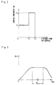
- the MESFET 1 is formed by epitaxial growth of a GaAs semiconductor material, and its active layer has a pulse-doped structure. That is, a doping profile below the gate electrode of the MESFET 1 is as shown in Fig. 2. Referring to Fig. 2, the abscissa indicates a distance from the surface to the interior of the GaAs semiconductor, and the ordinate indicates a carrier concentration. As graphically illustrated in Fig. 2, the carrier concentration remains at a concentration N1 from the surface to a predetermined depth D1 and increases stepwise to a concentration N2 in the predetermined depth D1.
- the shape of the profile is analogous to that of a pulse, and carriers are trapped in a pulse-doped GaAs layer from the depth D1 to D2 at the concentration N2. Since this pulse-doped GaAs layer is applied to the active layer of the MESFET 1, high-frequency characteristics and noise characteristics are improved.
- Fig, 3 shows the change in transconductance in the pulse-doped structure GaAs MESFET 1.
- the abscissa indicates a gate voltage V gs
- the ordinate indicates a transconductance g m .
- the transconductance g m remains at a constant value within a range A of the gate voltage V gs .
- Such a characteristic cannot be found in a MESFET or HEMT (High Electron Mobility Transistor), which is formed by ordinary ion implantation.
- the resistance of a gate bias resistor for determining the gate voltage of the MESFET 1, i.e., the resistance of the resistor 7 is set such that the gate voltage V gs has a voltage a within the range A.
- the present invention can be applied more effectively to high-frequency oscillators such as a voltage-controlled oscillator (VCO) which cannot use such a dielectric resonator. That is, although a dielectric resonator contributes to FM noise reduction to some extent, the present invention proves its merits when used in strict conditions where no dielectric resonator can be used.
- VCO voltage-controlled oscillator
Landscapes
- Inductance-Capacitance Distribution Constants And Capacitance-Resistance Oscillators (AREA)
Applications Claiming Priority (2)
| Application Number | Priority Date | Filing Date | Title |
|---|---|---|---|
| JP2311059A JP2932682B2 (ja) | 1990-11-16 | 1990-11-16 | 高周波発振回路 |
| JP311059/90 | 1990-11-16 |
Publications (2)
| Publication Number | Publication Date |
|---|---|
| EP0486062A1 true EP0486062A1 (fr) | 1992-05-20 |
| EP0486062B1 EP0486062B1 (fr) | 1997-04-16 |
Family
ID=18012620
Family Applications (1)
| Application Number | Title | Priority Date | Filing Date |
|---|---|---|---|
| EP91119562A Expired - Lifetime EP0486062B1 (fr) | 1990-11-16 | 1991-11-15 | Oscillateur haute fréquence |
Country Status (5)
| Country | Link |
|---|---|
| US (1) | US5164686A (fr) |
| EP (1) | EP0486062B1 (fr) |
| JP (1) | JP2932682B2 (fr) |
| CA (1) | CA2055663C (fr) |
| DE (1) | DE69125688T2 (fr) |
Cited By (1)
| Publication number | Priority date | Publication date | Assignee | Title |
|---|---|---|---|---|
| EP0551857A3 (en) * | 1992-01-14 | 1993-10-27 | Sumitomo Electric Industries | Mixer circuit using pulse-doped gaas mesfet |
Families Citing this family (7)
| Publication number | Priority date | Publication date | Assignee | Title |
|---|---|---|---|---|
| JPH04117805A (ja) * | 1990-09-07 | 1992-04-17 | Matsushita Electric Ind Co Ltd | 高周波電圧制御発振器 |
| US5602501A (en) * | 1992-09-03 | 1997-02-11 | Sumitomo Electric Industries, Ltd. | Mixer circuit using a dual gate field effect transistor |
| JP3148010B2 (ja) * | 1992-09-11 | 2001-03-19 | 住友電気工業株式会社 | ミキサ回路 |
| JPH08148933A (ja) * | 1994-11-22 | 1996-06-07 | Murata Mfg Co Ltd | 電圧制御型発振器 |
| DE19702261C2 (de) * | 1997-01-23 | 2000-02-03 | Grieshaber Vega Kg | Mikrowellen-Pulsgenerator |
| US6150680A (en) * | 1998-03-05 | 2000-11-21 | Welch Allyn, Inc. | Field effect semiconductor device having dipole barrier |
| JP5127362B2 (ja) * | 2007-08-23 | 2013-01-23 | 三菱電機株式会社 | 2倍波発振器 |
Family Cites Families (1)
| Publication number | Priority date | Publication date | Assignee | Title |
|---|---|---|---|---|
| EP0202652B2 (fr) * | 1985-05-21 | 1999-03-17 | Matsushita Electric Industrial Co., Ltd. | Oscillateur à hyperfréquence |
-
1990
- 1990-11-16 JP JP2311059A patent/JP2932682B2/ja not_active Expired - Lifetime
-
1991
- 1991-11-15 EP EP91119562A patent/EP0486062B1/fr not_active Expired - Lifetime
- 1991-11-15 CA CA002055663A patent/CA2055663C/fr not_active Expired - Fee Related
- 1991-11-15 US US07/791,738 patent/US5164686A/en not_active Expired - Lifetime
- 1991-11-15 DE DE69125688T patent/DE69125688T2/de not_active Expired - Fee Related
Non-Patent Citations (4)
| Title |
|---|
| ELECTRONICS & COMMUNICATIONS IN JAPAN vol. 63-B, no. 5, 1980, SIVER SPRING US pages 65 - 72; T. HAYASAKI ET AL.: 'MICROWAVE TRANSMISSION-TYPE DIELECTRIC RESONATOR TRANSISTOR OSCILLATOR' * |
| IEE PROCEEDINGS I. SOLID- STATE & ELECTRON DEVICES. vol. 127, no. 5, October 1980, STEVENAGE GB pages 241 - 249; C. TSIRONIS ET AL.: 'GUNN OSCILLATIONS IN THIN GaAs EPILAYERS AND m.e.s.f.e.t.s' * |
| PATENT ABSTRACTS OF JAPAN vol. 3, no. 71 (E-118)(121) 20 June 1979 & JP-A-54 051 361 ( NIPPON DENKI K.K. ) * |
| TRANSACTIONS OF THE IECE OF JAPAN vol. E63, no. 5, May 1980, TOKYO JP pages 378 - 379; T. HAYASAKI ET AL.: 'MICROWAVE TRANSMISSION-TYPE DIELECTRIC RESONATOR TRANSISTOR OSCILLATOR' * |
Cited By (1)
| Publication number | Priority date | Publication date | Assignee | Title |
|---|---|---|---|---|
| EP0551857A3 (en) * | 1992-01-14 | 1993-10-27 | Sumitomo Electric Industries | Mixer circuit using pulse-doped gaas mesfet |
Also Published As
| Publication number | Publication date |
|---|---|
| CA2055663C (fr) | 1995-07-18 |
| EP0486062B1 (fr) | 1997-04-16 |
| DE69125688T2 (de) | 1998-01-02 |
| CA2055663A1 (fr) | 1992-05-17 |
| JP2932682B2 (ja) | 1999-08-09 |
| DE69125688D1 (de) | 1997-05-22 |
| US5164686A (en) | 1992-11-17 |
| JPH04183006A (ja) | 1992-06-30 |
Similar Documents
| Publication | Publication Date | Title |
|---|---|---|
| US5347149A (en) | Integrated circuit and method | |
| US5055889A (en) | Lateral varactor with staggered punch-through and method of fabrication | |
| EP0854570A2 (fr) | Circuit pour stabiliser la polarisation | |
| US4481487A (en) | Monolithic microwave wide-band VCO | |
| EP0347111A2 (fr) | Dispositif à transistor à effet de champ métal-semi-conducteur | |
| US4605909A (en) | Dual gate FET oscillator mixer | |
| US6066997A (en) | Frequency multiplier with fundamental wave reflection | |
| US5164686A (en) | High-frequency oscillator having a field-effect transistor with a stepwise increasing active layer carrier concentration | |
| US4163984A (en) | Field effect transistor | |
| US4709251A (en) | Double Schottky-gate field effect transistor | |
| US4698654A (en) | Field effect transistor with a submicron vertical structure and its production process | |
| EP0587136A2 (fr) | Circuit mélangeur | |
| US4551904A (en) | Opposed gate-source transistor | |
| US5602501A (en) | Mixer circuit using a dual gate field effect transistor | |
| Phillippe et al. | Physical equivalent circuit model for planar Schottky varactor diode | |
| US5248948A (en) | Oscillating circuit device with a variable capacitor | |
| Siweris et al. | A monolithic W-band HEMT VCO with feedback topology | |
| EP0510709A1 (fr) | Circuit oscillateur | |
| US20020093388A1 (en) | Voltage-controlled oscillator and communication device | |
| US4951099A (en) | Opposed gate-source transistor | |
| US5159346A (en) | Voltage controlled oscillator | |
| EP0072647B1 (fr) | Ajustage de varacteur pour MMICS | |
| US4719434A (en) | Varactor trimming for MMICs | |
| US4608583A (en) | FET amplifier | |
| Sugiura et al. | 12-GHz-band low-noise GaAs monolithic amplifiers |
Legal Events
| Date | Code | Title | Description |
|---|---|---|---|
| PUAI | Public reference made under article 153(3) epc to a published international application that has entered the european phase |
Free format text: ORIGINAL CODE: 0009012 |
|
| AK | Designated contracting states |
Kind code of ref document: A1 Designated state(s): DE FR GB NL SE |
|
| 17P | Request for examination filed |
Effective date: 19921119 |
|
| 17Q | First examination report despatched |
Effective date: 19941213 |
|
| GRAG | Despatch of communication of intention to grant |
Free format text: ORIGINAL CODE: EPIDOS AGRA |
|
| GRAH | Despatch of communication of intention to grant a patent |
Free format text: ORIGINAL CODE: EPIDOS IGRA |
|
| GRAH | Despatch of communication of intention to grant a patent |
Free format text: ORIGINAL CODE: EPIDOS IGRA |
|
| GRAA | (expected) grant |
Free format text: ORIGINAL CODE: 0009210 |
|
| AK | Designated contracting states |
Kind code of ref document: B1 Designated state(s): DE FR GB NL SE |
|
| REF | Corresponds to: |
Ref document number: 69125688 Country of ref document: DE Date of ref document: 19970522 |
|
| ET | Fr: translation filed | ||
| PLBE | No opposition filed within time limit |
Free format text: ORIGINAL CODE: 0009261 |
|
| STAA | Information on the status of an ep patent application or granted ep patent |
Free format text: STATUS: NO OPPOSITION FILED WITHIN TIME LIMIT |
|
| 26N | No opposition filed | ||
| PGFP | Annual fee paid to national office [announced via postgrant information from national office to epo] |
Ref country code: SE Payment date: 20011106 Year of fee payment: 11 |
|
| PGFP | Annual fee paid to national office [announced via postgrant information from national office to epo] |
Ref country code: FR Payment date: 20011113 Year of fee payment: 11 |
|
| PGFP | Annual fee paid to national office [announced via postgrant information from national office to epo] |
Ref country code: NL Payment date: 20011129 Year of fee payment: 11 |
|
| PGFP | Annual fee paid to national office [announced via postgrant information from national office to epo] |
Ref country code: DE Payment date: 20011203 Year of fee payment: 11 |
|
| REG | Reference to a national code |
Ref country code: GB Ref legal event code: IF02 |
|
| PG25 | Lapsed in a contracting state [announced via postgrant information from national office to epo] |
Ref country code: SE Free format text: LAPSE BECAUSE OF NON-PAYMENT OF DUE FEES Effective date: 20021116 |
|
| PG25 | Lapsed in a contracting state [announced via postgrant information from national office to epo] |
Ref country code: NL Free format text: LAPSE BECAUSE OF NON-PAYMENT OF DUE FEES Effective date: 20030601 |
|
| PG25 | Lapsed in a contracting state [announced via postgrant information from national office to epo] |
Ref country code: DE Free format text: LAPSE BECAUSE OF NON-PAYMENT OF DUE FEES Effective date: 20030603 |
|
| EUG | Se: european patent has lapsed | ||
| PG25 | Lapsed in a contracting state [announced via postgrant information from national office to epo] |
Ref country code: FR Free format text: LAPSE BECAUSE OF NON-PAYMENT OF DUE FEES Effective date: 20030731 |
|
| NLV4 | Nl: lapsed or anulled due to non-payment of the annual fee |
Effective date: 20030601 |
|
| REG | Reference to a national code |
Ref country code: FR Ref legal event code: ST |
|
| PGFP | Annual fee paid to national office [announced via postgrant information from national office to epo] |
Ref country code: GB Payment date: 20051109 Year of fee payment: 15 |
|
| GBPC | Gb: european patent ceased through non-payment of renewal fee |
Effective date: 20061115 |
|
| PG25 | Lapsed in a contracting state [announced via postgrant information from national office to epo] |
Ref country code: GB Free format text: LAPSE BECAUSE OF NON-PAYMENT OF DUE FEES Effective date: 20061115 |