EP0486114A2 - Elektrischer Testapparat - Google Patents
Elektrischer Testapparat Download PDFInfo
- Publication number
- EP0486114A2 EP0486114A2 EP19910202975 EP91202975A EP0486114A2 EP 0486114 A2 EP0486114 A2 EP 0486114A2 EP 19910202975 EP19910202975 EP 19910202975 EP 91202975 A EP91202975 A EP 91202975A EP 0486114 A2 EP0486114 A2 EP 0486114A2
- Authority
- EP
- European Patent Office
- Prior art keywords
- circuit
- voltage
- current
- tested
- output
- Prior art date
- Legal status (The legal status is an assumption and is not a legal conclusion. Google has not performed a legal analysis and makes no representation as to the accuracy of the status listed.)
- Withdrawn
Links
- 238000012360 testing method Methods 0.000 title claims abstract description 42
- 230000008859 change Effects 0.000 claims description 12
- 238000001514 detection method Methods 0.000 claims description 2
- 230000002265 prevention Effects 0.000 claims description 2
- 238000009413 insulation Methods 0.000 description 17
- 230000004048 modification Effects 0.000 description 12
- 238000012986 modification Methods 0.000 description 12
- 239000003990 capacitor Substances 0.000 description 8
- 230000035945 sensitivity Effects 0.000 description 8
- 238000010586 diagram Methods 0.000 description 7
- 238000000034 method Methods 0.000 description 5
- 230000015556 catabolic process Effects 0.000 description 4
- 230000001419 dependent effect Effects 0.000 description 3
- 230000000694 effects Effects 0.000 description 3
- 238000005259 measurement Methods 0.000 description 3
- 230000000712 assembly Effects 0.000 description 2
- 238000000429 assembly Methods 0.000 description 2
- 230000007423 decrease Effects 0.000 description 2
- 230000009467 reduction Effects 0.000 description 2
- 230000001133 acceleration Effects 0.000 description 1
- 230000009471 action Effects 0.000 description 1
- 239000004020 conductor Substances 0.000 description 1
- 238000013461 design Methods 0.000 description 1
- 238000001914 filtration Methods 0.000 description 1
- 239000012212 insulator Substances 0.000 description 1
- 238000000691 measurement method Methods 0.000 description 1
- 230000008569 process Effects 0.000 description 1
- 230000004044 response Effects 0.000 description 1
Images


Classifications
-
- G—PHYSICS
- G01—MEASURING; TESTING
- G01R—MEASURING ELECTRIC VARIABLES; MEASURING MAGNETIC VARIABLES
- G01R31/00—Arrangements for testing electric properties; Arrangements for locating electric faults; Arrangements for electrical testing characterised by what is being tested not provided for elsewhere
- G01R31/50—Testing of electric apparatus, lines, cables or components for short-circuits, continuity, leakage current or incorrect line connections
Definitions
- This invention relates to electrical current measurement and more particularly to electrical current measurement for testing the insulation and continuity of electrical equipment.
- Insulation generally has high resistance values, commonly several megohms. Consequently, high voltages need to be applied to the circuit that is being tested in order to firstly subject the circuit to a voltage at which significant insulation breakdown may occur, and secondly to produce a high, and therefore more easily detectable, leakage current indicative of the quality of the insulation resistance.
- Insulation testing can be performed with an instrument commonly known as a 'Megger'. This instrument has the capability to produce high voltages, for example, 500V dc, and also a means of detecting current flow due to the applied high voltage. It is important to note that with this instrument that any current flow is considered to be leakage current, and that when testing a perfect insulator, the current flow should always be zero.
- Continuity between two points in a circuit is normally defined, like insulation, in terms of resistance.
- insulation resistances are of the order of Megohms
- continuity resistances are usually of fractions of an Ohm.
- the usual method of measuring such low resistances is to apply a high current, such as 1 Amp, to the circuit under test.
- a continuity resistance of 100 milliohms will produce a voltage difference either end of the conductor of 100 millivolts. This can be easily detected and measured using a digital volt meter. This is most accurately accomplished using what is known as the 'four-wire' configuration.
- an apparatus for testing an electrical circuit comprising:
- Voltage supply means for supplying a voltage and having a high voltage rail and a low voltage rail, characterised by the provision of; a monitor circuit, having a first and a second half; current supply means, for supplying an input current of equal magnitude to each half of said monitor circuit; connection means, for connecting a circuit to be tested to the first half of the monitor circuit; current varying means, for varying the input current, supplied to the first and second halves of the monitor circuit so as to maintain an output current from the circuit to be tested constant irrespective of any leakage losses in the circuit to be tested and to increase the current in the second half of the monitor circuit in proportion to the magnitude of the leakage loss in the circuit to be tested; and first connection means for connecting a first voltage measuring means for measuring the voltage across the first and second halves of the monitor circuit thereby to determine the magnitude of the leakage losses in the circuit to be tested.
- the apparatus includes a second voltage measuring means for measuring the voltage at a point in the first half of the monitor circuit thereby to determine the magnitude of continuity failure in the circuit to be tested.
- the apparatus includes prevention means for preventing the connection of a voltage supplied to the first voltage measuring means unless said voltage is within a predetermined range of voltages.
- Voltage modifying means may be provided for for modifying a voltage supplied to the first measuring means so as to provide a voltage in direct proportionality to the leakage loss.
- a high voltage diode may be connected between the output of the current supply means and the circuit to be tested so as to prevent possible damage to the current supply.
- a Zener diode may be connected at one end to the voltage supply means and at another end to the second half of the monitor circuit in order to prevent circuit damage.
- low pass filters are provided on each of the first and second halves of the monitor circuit in order to reduce the problems associated with induced electrical noise.
- a comparator may be connected to the first half of the monitor circuit and operable to change state upon detection of a change in continuity in the circuit to be tested.
- a constant current source is connected between the circuit to be tested and a point at which the first voltage measuring means is connected to the first half of the monitor circuit thereby to make the output current from the circuit to be tested and the current in the second half of the monitor circuit substantially immune to variations in the voltage supply from the voltage supply means.
- the current supply means is a current mirror.
- the apparatus may be additionally provided with a first amplifier the inputs of which are connected to the first and second halves of the monitor circuit and the output of which is connected to the gate of a source - follower connected JFET, the drain of said JFET being connected to the output of the current supply means and the high voltage rail of voltage supply and the source of the JFET being connected to the low voltage rail via a resistance across which the first voltage means may be connected for measuring the leakage loss in the circuit to be tested.
- the apparatus may be additionally provided with a first amplifier the inputs of which are connected to the first and second halves of the monitor circuit and the output of which is connected to the gate of a source - follower connected JFET, the drain of said JFET being connected to the output of the current supply means and the high voltage rail of the voltage supply and the source of the JFET being connected to the low voltage rail via a second amplifier such that the first voltage means may be connected between the output of said second amplifier and the low voltage rail so as to determine the leakage loss in the circuit to be tested.
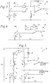
- the circuit shown generally at 1 includes a four-transistor PNP current mirror 2, a description of which can be found in "Current Mirrors, Amplifiers and Dumpers", Wireless World, December 1981 pages 47-50.
- the current mirror 2 is connected to a high voltage supply having a value V HT , and has one input and one output having current values I S and I O respectively.
- the input of the current mirror 2 is connected in series to the input of the circuit under test 3 (shown as a single wire for simplicity).
- the circuit under test 3 has a leakage current value I L and an output current value I R .
- the output of the circuit under test 3 is connected to the O volt return line via resistors 4 and 5 connected in series and having values R A and R X respectively.
- the output of current mirror 2 is also connected to the O volt return line via two resistors 6 and 7 connected in series and having values R B and R Y respectively.
- the system output i.e. a representation of leakage current I L , is taken from two terminals 8 and 9 positioned between the series resistor pairs 4, 5 and 6, 7 respectively.
- the two resistors 4 and 6 operate as buffer resistors for attenuating the high voltage V HT .
- the value R A of resistor 4 is chosen to set the value of the bias current I S from the current mirror.
- the value R B of resistor 6 is chosen carefully so that the collector voltage swing of the current mirror output transistor remains within its normal operating parameters for the range of values that the output current may take in response to current leakage.
- V Y would decrease by the amount I L x R Y .
- the circuit 1 is effectively split into two halves.
- the first half is connected to the input I S of the current mirror 2 and includes the circuit under test 3, and the second half is connected to the output I O of the current mirror 2 and provides an output voltage indicative of the leakage current.
- the two halves are almost independent, being linked only by the current mirror 2.
- altering parameters in the one half of the circuit will have negligible effect on the other half.
- the circuit has been described with a differential output, i.e. measuring the voltage difference between each half of the circuit 1, it should be appreciated that a single output from terminal 9 could be used.
- the differential output is equal to I L x R Y , and therefore is only dependent on the change of current value I L (the resistance value R Y being constant) and not on the bias current I S .
- the differential output also gives common-mode rejection. Any supply voltage ripple would result in a change of current I S , but this change would be "mirrored" by the current mirror 2 in current I O .
- R X is equal to R Y , then the changes in voltages V X and V Y will cancel one another out.
- the ratio of leakage current I L to bias current I S is high.
- the bias current I S is chosen to be at least ten times greater than the expected leakage current.
- a continuity test may also be performed by measuring the voltage V X at terminal 8. For a total continuity failure, V X would fall to OV as would V Y . A partial continuity failure would result in a reduction of current I R and voltage V X , the amount of reduction being dependent of the ratio of the effective continuity resistance of the test circuit 3 to the value R A of resistor 4. It should be noted that a partial continuity failure will result in change in current I S which will be "mirrored" by the current mirror 2 in current I O , hence the differential voltage output, which represents leakage current, will not change. Thus, the circuit 1 clearly establishes whether change in output at terminals 8 and 9 is due to a continuity or insulation failure condition.
- a circuit adapted for testing if the leakage current is within a predetermined range is shown generally at 10.
- This circuit includes all the components of the circuit of Figure 1 above the line A-A and is modified below this line as shown.
- This circuit is operable for determining whether the leakage current is outside a predetermined value.
- the basic circuit is the same as that of Figure 1. However, the output from the terminal 8 is connected to voltage buffer 11, the output of which is in turn connected in parallel to two diodes 12 and 13. These diodes set the limits of the positive and negative voltage which is to be measured.
- the value range for which the circuit will produce an output is adjusted between these values by two potentiometers 14 and 15 connected in parallel across the diode pair 12 and 13.
- Output terminal 9 is connected to the input of each of two comparators 16 and 17, while the reference voltage input of each of the two comparators is supplied by the output of respective potentiometers 14 and 15.
- a voltage "window" can be set in which the comparators give an output indicative of a leakage current.
- the window may be simply changed in size by adjusting each of the two potentiometers 14 and 15.
- a circuit adapted to give an output directly proportional to the leakage current is shown generally at 20.
- This circuit includes all the components of the circuit shown in Figure 1 above the line A-A and is modified below this line as shown.
- the basic circuit is again the same as that of Figure 1.
- the resistors 5, 7, 21, 23, 24 and 25 must be matched to provide common-mode rejection.
- a circuit having an equivalent function to that of the circuit 20 is shown in Figure 4 at 26.
- the circuit uses fewer components - resistors 7, 21, 23 and 25 are dispensed with - and, provided the value R X of resistor 5 and the value R Y of resistor 24 are matched the circuit will give common mode rejection. Under no leakage current conditions, the voltage V q is essentially zero.
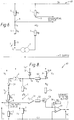
- the first modification consists of a high-voltage diode 31 inserted between the input of the current mirror 2 and the circuit under test 3.
- This modification is desirable when, for example, the test circuit consists of several cable wires which are tested simultaneously and in which there is a short circuit fault between two or more wires that are at a different potential to one another. If the diode 31 was not present, then the input transistor of the current mirror, when at the lowest potential, may be reverse biased thus possibly destroying it. However the inclusion of the diode 31 will reduce the voltage on the circuit under test by one Vbe (the base-emitter voltage of the current mirror transistors). The value of Vbe is essentially constant for a wide range of values for the current I S , but can be compensated for, if necessary, by an increase of applied voltage V HT .
- the second modification consists of a Zener diode 32 placed between the current mirror input I O and the high voltage supply V HT .
- the Zener diode 32 has a value chosen to be near the breakdown voltage of the output transistor of the current mirror 2. This modification is desirable when a continuity failure occurs in the circuit under test 3 because this causes the current mirror 2 currents I S and I O to fall to essentially zero. This would cause the output transistor of the current mirror to cut-off and, if the applied voltage is greater than the transistor collector breakdown voltage, then the output transistor could be destroyed.
- the Zener diode 32 provides an alternative electrical path that conducts before the collector voltage reaches its breakdown value. In some applications the Zener diode 32 could be replaced by a resistor. However, this may result in a significant error in the value of current I O - much larger than the relatively small error caused by the Zener diode 32.
- the third modification consists of two capacitors 33 and 34.
- Capacitor 33 is inserted in parallel across resistor 5 and Capacitor 34 is inserted in parallel across resistor 7.
- the capacitors 33 and 34 act as low pass filters on the two output terminals 8 and 9.
- the values of the capacitors required depend on the values R A , R B of the two resistors 4 and 6 and should ideally be selected such that the values of resistor 4 and capacitor 33 have an equal time constant to resistor 6 and capacitor 34.
- the inclusion of the capacitors reduce the problems associated with induced electrical noise in the circuit under test 3 without the problems associated with changing the value of R Y of resistor 7. Many other filtering methods could equally well be used.
- the fourth modification consists of connecting the inverting input of a comparator 35 to the continuity detector output from terminal 8 and connecting the reference voltage input to a constant voltage supply having a value V R which is between OV and the voltage V X under normal continuity conditions. If a discontinuity occurs in the circuit under test 3 then the current I S falls to zero as does V X . The comparator 35 will respond to this by changing state. Thus, the comparator 35 provides a simple continuity check performed on the circuit under test 3 at the same time as the insulation test. The circuit does not monitor continuity in terms of absolute resistance but it does perform a simple open-circuit/short-circuit check which in many situations is sufficient.
- the sensitivity is set by the voltage difference at the comparator inputs. In order that the comparator 35 does not change state due to noise or other unwanted signals, the sensitivity should be set low by making V R at least several hundred millivolts less that V X .
- a fifth modification consists of a constant current source 36, having a constant current output equal to I R , which replaces the link between resistor 4 and terminal 8.
- the constant current source 36 has the effect of making the currents I R , and therefore I O , virtually immune from any variations of the high voltage supply V HT .
- the bias current is set by the current source - rather than by the high voltage supply and the value R A of resistor 4 as in previously described embodiments.
- Figure 6 shows an alternative embodiment of the invention.
- the circuit, shown generally at 40 is effectively an inversion of the Figure 1 circuit - the high voltage supply is now negative with respect to OV and the current mirror is a four transistor NPN type (rather that a PNP type).
- NPN current mirrors are available in 'chip' form (for example, the Burr Brown REF 200) and, furthermore, NPN current mirrors may have a more accurate operation than the PNP type.
- FIG. 7 shows a further embodiment of the invention.
- the circuit shown generally at 50, overcomes the problem of inaccuracy when used with high supply voltages as previously described in relation to Figure 1.
- the basic circuit is the same as that of Figure 1.
- Terminals 8 and 9 are connected to the inverting and non-inverting inputs of amplifier 51 respectively.
- the output of amplifier 51 is applied, via a resistor 52, to the gate of a source - follower connected JFET 53.
- the output of the current mirror 2 is connected to the drain of the JFET 53 via a resistor 54.
- the high voltage source V HT is also applied to the drain of the JFET 53 via two resistors 54 and 55, the latter having a resistance value RD.
- the source of JFET 53 is connected to the OV supply rail via a resistor 56 (value R O ) across which the voltage V O (representing leakage current I L ) can be measured.
- resistors R X and R Y are selected as before, but the values R A and R B are not as critical as they were in the circuit of Figure 1, although they must have equal values selected to ensure the current mirror 2 operates well within its range.
- resistor R O sets the sensitivity of the circuit, and can simply be adjusted without affecting the common mode rejection quality of output.
- Figure 8 shows yet a further embodiment of the invention.
- the circuit shown generally at 60 is based on the circuit of Figure 7.
- the circuits differ in the following ways.
- the source of the source-follower 53 is connected to the inverting input of amplifier 61, while the non-inverting input is connected to the OV supply line.
- the inverting input and the output of amplifier 61 are connected by means of a resistor 56 (value R O ).
- the configuration ensures that the gate voltage of the JFET 53 is always maintained within the output voltage range of amplifier 51, assuming the JFET 53 has a fairly low 'pinch-off' voltage.
- the circuit of Figure 8 also includes diodes 31 and 32 which operates in the same way as their identically labelled counterparts described in relation to Figure 5.
- the diode 31 adds approximately 0.6v to the value of V T . This can, however, be compensated for by a suitable increase in the value of R B .
- Another modification to the circuit is the inclusion of resistor 62 (value Re). This resistor is included to add current gain to the circuit which provides an alternative method of controlling the output gain of the circuit.
Landscapes
- Physics & Mathematics (AREA)
- General Physics & Mathematics (AREA)
- Testing Of Short-Circuits, Discontinuities, Leakage, Or Incorrect Line Connections (AREA)
- Testing Relating To Insulation (AREA)
Applications Claiming Priority (2)
| Application Number | Priority Date | Filing Date | Title |
|---|---|---|---|
| GB909024912A GB9024912D0 (en) | 1990-11-16 | 1990-11-16 | Electrical testing apparatus |
| GB9024912 | 1990-11-16 |
Publications (2)
| Publication Number | Publication Date |
|---|---|
| EP0486114A2 true EP0486114A2 (de) | 1992-05-20 |
| EP0486114A3 EP0486114A3 (en) | 1992-10-28 |
Family
ID=10685463
Family Applications (1)
| Application Number | Title | Priority Date | Filing Date |
|---|---|---|---|
| EP19910202975 Withdrawn EP0486114A3 (en) | 1990-11-16 | 1991-11-15 | Electrical testing apparatus |
Country Status (5)
| Country | Link |
|---|---|
| EP (1) | EP0486114A3 (de) |
| JP (1) | JPH05196678A (de) |
| AU (1) | AU8780691A (de) |
| CA (1) | CA2055641A1 (de) |
| GB (2) | GB9024912D0 (de) |
Cited By (3)
| Publication number | Priority date | Publication date | Assignee | Title |
|---|---|---|---|---|
| EP0689058A2 (de) | 1994-06-24 | 1995-12-27 | Philips Patentverwaltung GmbH | Schaltungsanordnung zum Überwachen eines Schaltungspunktes auf einen Leckwiderstand |
| DE19526435A1 (de) * | 1995-06-01 | 1996-12-19 | Teves Gmbh Alfred | Schaltungsanordnung zur Fehlerstromerkennung |
| US11372056B2 (en) * | 2020-05-26 | 2022-06-28 | Sandisk Technologies Llc | Circuit for detecting pin-to-pin leaks of an integrated circuit package |
Families Citing this family (1)
| Publication number | Priority date | Publication date | Assignee | Title |
|---|---|---|---|---|
| DE29505412U1 (de) * | 1995-03-30 | 1996-05-02 | Siemens AG, 80333 München | Vorrichtung zur potentialgetrennten Kabelbrucherkennung bei digitalen Übertragungsstrecken mit symmetrischer Übertragung, insbesondere für digitale Wegmeßgeber |
-
1990
- 1990-11-16 GB GB909024912A patent/GB9024912D0/en active Pending
-
1991
- 1991-11-12 AU AU87806/91A patent/AU8780691A/en not_active Abandoned
- 1991-11-13 GB GB9124050A patent/GB2250100A/en not_active Withdrawn
- 1991-11-15 CA CA002055641A patent/CA2055641A1/en not_active Abandoned
- 1991-11-15 EP EP19910202975 patent/EP0486114A3/en not_active Withdrawn
- 1991-11-16 JP JP3300900A patent/JPH05196678A/ja active Pending
Non-Patent Citations (3)
| Title |
|---|
| IBM TECHNICAL DISCLOSURE BULLETIN. vol. 21, no. 1, June 1978, NEW YORK US pages 111 - 112; CARROLL: 'DIFFERENTIAL VOLTAGE DETECTOR' * |
| NEW ELECTRONICS.INCORPORATING ELECTRONICS TODAY. vol. 9, no. 18, 21 September 1976, LONDON GB page 34; MEEK: 'MEASUREMENT OF CONTACT BOUNCE' * |
| WIRELESS WORLD. December 1981, HAYWARDS HEATH GB pages 47 - 50; WILSON: 'CURRENT MIRRORS, AMPLIFIERS AND DUMPERS' * |
Cited By (6)
| Publication number | Priority date | Publication date | Assignee | Title |
|---|---|---|---|---|
| EP0689058A2 (de) | 1994-06-24 | 1995-12-27 | Philips Patentverwaltung GmbH | Schaltungsanordnung zum Überwachen eines Schaltungspunktes auf einen Leckwiderstand |
| EP0689058A3 (de) * | 1994-06-24 | 1997-05-21 | Koninkl Philips Electronics Nv | Schaltungsanordnung zum Überwachen eines Schaltungspunktes auf einen Leckwiderstand |
| US5640095A (en) * | 1994-06-24 | 1997-06-17 | U.S. Philips Corp. | Circuit arrangement for leakage-resistance testing of a circuit point |
| DE19526435A1 (de) * | 1995-06-01 | 1996-12-19 | Teves Gmbh Alfred | Schaltungsanordnung zur Fehlerstromerkennung |
| DE19526435B4 (de) * | 1995-06-01 | 2004-07-22 | Continental Teves Ag & Co. Ohg | Schaltungsanordnung zur Fehlerstromerkennung |
| US11372056B2 (en) * | 2020-05-26 | 2022-06-28 | Sandisk Technologies Llc | Circuit for detecting pin-to-pin leaks of an integrated circuit package |
Also Published As
| Publication number | Publication date |
|---|---|
| GB9124050D0 (en) | 1992-01-02 |
| GB9024912D0 (en) | 1991-01-02 |
| GB2250100A (en) | 1992-05-27 |
| JPH05196678A (ja) | 1993-08-06 |
| EP0486114A3 (en) | 1992-10-28 |
| AU8780691A (en) | 1992-05-21 |
| CA2055641A1 (en) | 1992-05-17 |
Similar Documents
| Publication | Publication Date | Title |
|---|---|---|
| CA1199069A (en) | Active voltage probe | |
| US4278931A (en) | Location of contact faults on electrically conductive cables | |
| US5359291A (en) | Method and apparatus for detecting short circuits | |
| US3784906A (en) | Bridge having multiple nulls | |
| DE69021036T2 (de) | Test-Anordnungssystem für integrierte Schaltungen unter Verwendung von lateralen Transistoren. | |
| US5272445A (en) | Resistance tester utilizing regulator circuits | |
| US5414348A (en) | Measurement device with common mode current cancellation | |
| EP0486114A2 (de) | Elektrischer Testapparat | |
| US6292342B1 (en) | Voltage protection circuit for semiconductor test system | |
| EP1618397B1 (de) | Messschaltungsanordnung mit erhöhter genauigkeit | |
| US5600249A (en) | Determining contact quality of an impedance meter | |
| JP2610640B2 (ja) | 自動車の少なくとも2つの電気的負荷を検査する装置 | |
| JPS6325572A (ja) | 電位計増幅器の漏洩電流測定システム | |
| US6611146B2 (en) | Stress testing for semiconductor devices | |
| US6483318B1 (en) | Electric circuit providing selectable short circuit for instrumentation applications | |
| JP2986804B2 (ja) | インサーキット機能試験装置及び方法 | |
| US6462528B1 (en) | Method and apparatus for probing a conductor of an array of closely-spaced conductors | |
| US3541436A (en) | Resistance indicator using an operational amplifier | |
| US3437925A (en) | Circuit for converting resistance values of unknown resistor to electrical potential signal for measurement purposes | |
| KR100352598B1 (ko) | 디지털멀티메터입력자동제어장치 | |
| KR890004530Y1 (ko) | 트랜지스터의 전류이득률 측정회로 | |
| US3654550A (en) | Kelvin double bridge with zener diode failure circuit | |
| DE29705598U1 (de) | Dreileiterschaltung für Widerstandsthermometer | |
| JPS5820942Y2 (ja) | 電源試験用負荷装置 | |
| JP3147486B2 (ja) | 半導体素子測定回路 |
Legal Events
| Date | Code | Title | Description |
|---|---|---|---|
| PUAI | Public reference made under article 153(3) epc to a published international application that has entered the european phase |
Free format text: ORIGINAL CODE: 0009012 |
|
| 17P | Request for examination filed |
Effective date: 19911122 |
|
| AK | Designated contracting states |
Kind code of ref document: A2 Designated state(s): AT BE CH DE DK ES FR GB GR IT LI LU NL SE |
|
| PUAL | Search report despatched |
Free format text: ORIGINAL CODE: 0009013 |
|
| RAP3 | Party data changed (applicant data changed or rights of an application transferred) |
Owner name: BRITISH AEROSPACE PUBLIC LIMITED COMPANY |
|
| AK | Designated contracting states |
Kind code of ref document: A3 Designated state(s): AT BE CH DE DK ES FR GB GR IT LI LU NL SE |
|
| 17Q | First examination report despatched |
Effective date: 19940803 |
|
| STAA | Information on the status of an ep patent application or granted ep patent |
Free format text: STATUS: THE APPLICATION IS DEEMED TO BE WITHDRAWN |
|
| 18D | Application deemed to be withdrawn |
Effective date: 19950125 |