EP0486130B1 - Einphasige Leistungswandlereinrichtung - Google Patents
Einphasige Leistungswandlereinrichtung Download PDFInfo
- Publication number
- EP0486130B1 EP0486130B1 EP91305640A EP91305640A EP0486130B1 EP 0486130 B1 EP0486130 B1 EP 0486130B1 EP 91305640 A EP91305640 A EP 91305640A EP 91305640 A EP91305640 A EP 91305640A EP 0486130 B1 EP0486130 B1 EP 0486130B1
- Authority
- EP
- European Patent Office
- Prior art keywords
- voltage
- load
- power
- switching devices
- node
- Prior art date
- Legal status (The legal status is an assumption and is not a legal conclusion. Google has not performed a legal analysis and makes no representation as to the accuracy of the status listed.)
- Expired - Lifetime
Links
Images


Classifications
-
- H—ELECTRICITY
- H02—GENERATION; CONVERSION OR DISTRIBUTION OF ELECTRIC POWER
- H02J—ELECTRIC POWER NETWORKS; CIRCUIT ARRANGEMENTS OR SYSTEMS FOR SUPPLYING OR DISTRIBUTING ELECTRIC POWER; SYSTEMS FOR STORING ELECTRIC ENERGY
- H02J9/00—Circuit arrangements for emergency or stand-by power supply, e.g. for emergency lighting
- H02J9/04—Circuit arrangements for emergency or stand-by power supply, e.g. for emergency lighting in which the distribution system is disconnected from the normal source and connected to a standby source
- H02J9/06—Circuit arrangements for emergency or stand-by power supply, e.g. for emergency lighting in which the distribution system is disconnected from the normal source and connected to a standby source with automatic change-over, e.g. UPS systems
- H02J9/062—Circuit arrangements for emergency or stand-by power supply, e.g. for emergency lighting in which the distribution system is disconnected from the normal source and connected to a standby source with automatic change-over, e.g. UPS systems for AC powered loads
-
- H—ELECTRICITY
- H02—GENERATION; CONVERSION OR DISTRIBUTION OF ELECTRIC POWER
- H02M—APPARATUS FOR CONVERSION BETWEEN AC AND AC, BETWEEN AC AND DC, OR BETWEEN DC AND DC, AND FOR USE WITH MAINS OR SIMILAR POWER SUPPLY SYSTEMS; CONVERSION OF DC OR AC INPUT POWER INTO SURGE OUTPUT POWER; CONTROL OR REGULATION THEREOF
- H02M3/00—Conversion of DC power input into DC power output
-
- H—ELECTRICITY
- H02—GENERATION; CONVERSION OR DISTRIBUTION OF ELECTRIC POWER
- H02M—APPARATUS FOR CONVERSION BETWEEN AC AND AC, BETWEEN AC AND DC, OR BETWEEN DC AND DC, AND FOR USE WITH MAINS OR SIMILAR POWER SUPPLY SYSTEMS; CONVERSION OF DC OR AC INPUT POWER INTO SURGE OUTPUT POWER; CONTROL OR REGULATION THEREOF
- H02M5/00—Conversion of AC power input into AC power output, e.g. for change of voltage, for change of frequency, for change of number of phases
- H02M5/40—Conversion of AC power input into AC power output, e.g. for change of voltage, for change of frequency, for change of number of phases with intermediate conversion into DC
- H02M5/42—Conversion of AC power input into AC power output, e.g. for change of voltage, for change of frequency, for change of number of phases with intermediate conversion into DC by static converters
- H02M5/44—Conversion of AC power input into AC power output, e.g. for change of voltage, for change of frequency, for change of number of phases with intermediate conversion into DC by static converters using discharge tubes or semiconductor devices to convert the intermediate DC into AC
- H02M5/453—Conversion of AC power input into AC power output, e.g. for change of voltage, for change of frequency, for change of number of phases with intermediate conversion into DC by static converters using discharge tubes or semiconductor devices to convert the intermediate DC into AC using devices of a triode or transistor type requiring continuous application of a control signal
- H02M5/458—Conversion of AC power input into AC power output, e.g. for change of voltage, for change of frequency, for change of number of phases with intermediate conversion into DC by static converters using discharge tubes or semiconductor devices to convert the intermediate DC into AC using devices of a triode or transistor type requiring continuous application of a control signal using semiconductor devices only
-
- H—ELECTRICITY
- H02—GENERATION; CONVERSION OR DISTRIBUTION OF ELECTRIC POWER
- H02M—APPARATUS FOR CONVERSION BETWEEN AC AND AC, BETWEEN AC AND DC, OR BETWEEN DC AND DC, AND FOR USE WITH MAINS OR SIMILAR POWER SUPPLY SYSTEMS; CONVERSION OF DC OR AC INPUT POWER INTO SURGE OUTPUT POWER; CONTROL OR REGULATION THEREOF
- H02M7/00—Conversion of AC power input into DC power output; Conversion of DC power input into AC power output
- H02M7/42—Conversion of DC power input into AC power output without possibility of reversal
- H02M7/44—Conversion of DC power input into AC power output without possibility of reversal by static converters
- H02M7/48—Conversion of DC power input into AC power output without possibility of reversal by static converters using discharge tubes with control electrode or semiconductor devices with control electrode
- H02M7/53—Conversion of DC power input into AC power output without possibility of reversal by static converters using discharge tubes with control electrode or semiconductor devices with control electrode using devices of a triode or transistor type requiring continuous application of a control signal
- H02M7/537—Conversion of DC power input into AC power output without possibility of reversal by static converters using discharge tubes with control electrode or semiconductor devices with control electrode using devices of a triode or transistor type requiring continuous application of a control signal using semiconductor devices only, e.g. single switched pulse inverters
- H02M7/538—Conversion of DC power input into AC power output without possibility of reversal by static converters using discharge tubes with control electrode or semiconductor devices with control electrode using devices of a triode or transistor type requiring continuous application of a control signal using semiconductor devices only, e.g. single switched pulse inverters in a push-pull configuration
- H02M7/53803—Conversion of DC power input into AC power output without possibility of reversal by static converters using discharge tubes with control electrode or semiconductor devices with control electrode using devices of a triode or transistor type requiring continuous application of a control signal using semiconductor devices only, e.g. single switched pulse inverters in a push-pull configuration with automatic control of output voltage or current
-
- H—ELECTRICITY
- H02—GENERATION; CONVERSION OR DISTRIBUTION OF ELECTRIC POWER
- H02M—APPARATUS FOR CONVERSION BETWEEN AC AND AC, BETWEEN AC AND DC, OR BETWEEN DC AND DC, AND FOR USE WITH MAINS OR SIMILAR POWER SUPPLY SYSTEMS; CONVERSION OF DC OR AC INPUT POWER INTO SURGE OUTPUT POWER; CONTROL OR REGULATION THEREOF
- H02M1/00—Details of apparatus for conversion
- H02M1/0083—Converters characterised by their input or output configuration
- H02M1/0093—Converters characterised by their input or output configuration wherein the output is created by adding a regulated voltage to or subtracting it from an unregulated input
Definitions
- This invention pertains generally to the field of electrical power supplies and particularly to power supplies utilizing static power converters.
- a common solid state circuit structure for converting alternating current (AC) power to another frequency includes a rectifying bridge which converts the input AC voltage to a DC voltage on a DC link and a solid state inverter which inverts the DC voltage to AC power at a desired frequency.
- AC to AC power conversion includes a rectifying bridge which converts the input AC voltage to a DC voltage on a DC link and a solid state inverter which inverts the DC voltage to AC power at a desired frequency.
- a straightforward method for converting the output voltage level to a different level than that of the input voltage is a step up or step down transformer, either on the input or output side.
- transformers are relatively large, heavy and expensive.
- the power supply circuit is intended to allow the output voltage to be maintained at a desired level despite variations in the input voltage (or conversely, to allow the output voltage to be adjusted to a desired level at a constant input voltage)
- more complex transformer structures may be required.
- some power conditioning circuits utilize tap-changing transformers in which the primary includes a number of separate taps which are connected to the input terminals by static switches, with a control circuit monitoring the output voltage and switching the proper static switches on the input side to maintain approximately the desired voltage on the output side.
- Tap changing arrangements require many switches, such as thyristors, and only permit coarse control of the output voltage. Furthermore, the distortion of the voltage on the load cannot be well controlled.
- Line conditioning structure utilizes a ferroresonant transformer in which the transformer itself is connected in a circuit which provides passive compensation for short term changes in the input voltage.
- Ferroresonant transformers are widely used and give reasonable voltage regulation, typically plus or minus 4% at the output for minus 20% to plus 10% change in the input voltage.
- output distortion can be sensitive to load input harmonics, and the input currents drawn may have undesirable power factors and distortion levels.
- Both the tap changing and the ferroresonant transformers are restricted by the presence of the low frequency transformer which must be able to handle full rated power.
- the transformer for a 1 kilo volt ampere (KVA) line conditioner, the transformer by itself can weigh over thirty to forty pounds, and is the major component determining the size of the cabinet containing the power conditioning apparatus.
- KVA 1 kilo volt ampere
- the U.S. patent to Umezu , 4,656,571 uses a voltage doubler to increase the available AC output voltage.
- such circuits typically require that the input AC voltage be fully converted to a DC voltage level on a DC bus and then inverted to AC power utilizing a full bridge, for example, four switching devices to provide a single phase output voltage and six switching devices to provide a three phase output, as shown in the patent to Umezu .
- Static power converters are also commonly used in uninterruptible power systems (UPS) in which the converter operates to supply power to a load from the AC source during normal operation, switching to supply power from a storage device (e.g. a battery) connected across the DC bus lines during line power failure.
- UPS uninterruptible power systems
- a simple switching converter which provides UPS operation with only two inverter switches is shown in UK patent application GB 2,111, 326A to Berman , on which the precharacterising portion of appended claim 1 is based.
- single phase AC power conversion apparatus for converting power from an AC power source (21) at one frequency and voltage level to supply power to a load (22), comprising:
- a power conversion apparatus in accordance with the present invention may allow an AC source voltage at one voltage level to be converted to an output AC voltage at a different voltage level without a transformer and with a minimum of solid state switching devices.
- AC input power is converted to AC output power at the same frequency and without a full bridge conversion of the input AC to an intermediate DC voltage level.
- the apparatus can be embodied, for example, as a voltage doubler, can provide power conditioning to regulate the output voltage level despite changes in the input voltage level, and can further be configured as an uninterruptible power supply by providing a backup power source, e.g. a battery, from which power can be drawn to drive the input voltage if the input power fails.
- a backup power source e.g. a battery
- the three nodes can serve as the three terminals of the converter.
- the first terminal or node is common to both the input power source and the load, with the second node or terminal connected to the source and the third node or terminal connected to the load.
- the conversion circuit can be controlled to provide a peak-to-peak output voltage to the load which is substantially doubled from the peak-to-peak input voltage or, with a low pass filter connected to filter the output voltage to the load and to provide a substantially sinusoidal waveform, if desired, to control the output voltage applied to the load so that the voltage across the load can vary from substantially zero to substantially twice the peak-to-peak input voltage.
- the controller may provide turn-on and turn-off signals to the controllable switches alternately and in phase with the input voltage so that the voltage across one of the charged capacitors plus the input voltage is applied to the load during one-half cycle of the input power waveform, and with the voltage across the other charged capacitor and the input voltage of the opposite polarity applied to the load during the second half of the input voltage waveform.
- the switching devices may be switched on for a duty cycle which is less than a full half cycle of the input voltage waveform. For example, pulse width modulation may be utilized in switching the switching devices so that a desired effective AC voltage is provided across the load. Only two switching devices are required to obtain such operation.
- the power conversion apparatus of the present invention can be further extended to uninterruptible power supply operation by providing a DC power storage device across the DC bus lines which connect the pairs of switching devices.
- the storage device may be a large charged capacitor which can be charged up during normal input power conditions by utilizing switchable rectifying devices rather than passive rectifying devices.
- the use of active rather than passive devices also allows control of input current, attainment of unity power factor, and control of battery charging if a battery is substituted for the capacitor.
- the capacitor will provide sufficient power to allow voltage across the load to be maintained during momentary input power loss.
- a long-term storage device such as a storage battery can be connected across the DC bus and charged during periods of normal input power. During a power outage, the non-neutral input line can be disconnected from the conversion apparatus, and continuous power is then provided to the load from the battery.
- the conversion apparatus of the present invention provides a particularly simple circuit structure, requiring only two controllable switching devices to provide AC output power to the load and to allow control of the voltage level of that power to regulate the power level or to compensate for changes in the input voltage level utilizing relatively simple control implementations.
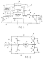
- Fig. 1 is a block diagram of the conversion apparatus of the present invention connected in an exemplary configuration to an input power source and to a load.
- Fig. 2 is a schematic circuit diagram of the conversion apparatus of the present invention connected to a load so as to achieve voltage doubler operation.
- Fig. 3 are exemplary voltage and current waveforms for the circuit of Fig. 2.
- Fig. 4 is an exemplary control circuit for the voltage doubler circuit of Fig. 3.
- Fig. 5 is a further control circuit for the voltage doubler circuit of Fig. 2.
- Fig. 6 is a schematic circuit diagram of the conversion apparatus of the invention configured to allow control of the voltage provided across the load.
- Fig. 7 is a schematic block diagram of a controller for controlling the switching of the switching devices in the circuit of Fig. 6 to provide feedback control of the voltage across the load.
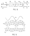
- Fig. 8 is a schematic block diagram of a sigma delta modulator which can be utilized in the controller of Fig. 7.
- Fig. 9 are graphs of exemplary voltage waveforms for the circuit of Fig. 6.
- Fig. 10 is a schematic circuit diagram of the conversion apparatus of the invention configured to provide uninterruptible power to the load during momentary input power loss.
- Fig. 11 is a schematic circuit diagram of the conversion apparatus of the invention configured to provide uninterruptible power to the load during long-term input power outages.
- Fig. 12 are graphs of exemplary supply voltage and line current waveforms for the circuits of Figs. 10 and 11.
- a generalized block diagram of the power conversion apparatus of the present invention is shown generally at 20 in Fig. 1 connected to receive alternating current (AC) voltage from a source 21 and to deliver AC power to a load 22.
- the apparatus 20 includes a conversion circuit indicated generally at 24 in Fig. 1 which has three terminals, labeled I, II, and III in Fig. 1.
- the source 21 is connected between the terminals I and II and the load is connected between the terminals I and III.
- a neutral line 26 connects the terminal I to the source 21 and a neutral line 41 connects the terminal I to the load 22.
- the conversion circuit 24 is adapted to receive the AC input voltage between the terminals I and II and deliver an AC output voltage of essentially the same frequency between the terminals I and III but at a voltage level which may differ from the voltage provided by the source.
- the operation of the conversion circuit 24 is controlled by a controller 28 which provides control signals on lines 29 to the conversion circuit 24.
- the controller 28 is shown as having lines 30 connected across the terminals I and II to sense the input voltage to the conversion circuit, lines 31 connected across the output terminals I and III to sense the output voltage, and a line 33 connected to a current transformer 34 which may be used to sense the current I L flowing to the load 22.
- the conversion circuit 24 can be controlled by the controller 28 to deliver an output voltage to the load 22 which is either twice the peak-to-peak source voltage V S or some lesser voltage which can be selected to a desired level and which can be regulated to maintain that level despite changes in the value of the source voltage or load current.
- a low pass filter circuit is preferably provided which is composed of a capacitor 36 connected across the terminals I and III and an inductor 37 connected in series with the load between the terminals I and III, with both the capacitor 36 and inductor 37 shown in dashed lines in Fig. 1. This LC filter serves to filter the modulated voltage provided from the conversion circuit 24.
- an optional energy storage device 39 connected to the conversion circuit 24 by lines 40, can provide temporary power to the conversion circuit to support the output voltage provided to the load during momentary breaks in the source voltage V S provided from the source 21.
- the energy storage device 39 can take the form of a large energy storage capacitor, which can be maintained charged during normal operation and discharged to carry the conversion circuit through short breaks, or a battery which provides longer term DC power to the conversion circuit.
- the conversion circuit 24 utilizes only passive components and electronic switches, and does not require transformers either to regulate the power provided to the load or allow adjustment of the level of the voltage provided to the load. A transformer could, however, be used if isolation was desired.
- FIG. 2 An implementation of the power supply apparatus of the present invention having a conversion circuit embodied as a voltage doubler is shown in Fig. 2.
- the input lines 26 and 27 providing the voltage V i from the source to the conversion circuit and the output lines 41 and 42 connecting the conversion circuit to the load are given the same reference numerals as in Fig. 1.
- the neutral input line 26 is connected to the first node, marked as the terminal or node I in Fig. 2, which joins a pair of rectifying devices (e.g., semiconductor diodes) 48 and 49 with the rectifying devices 48 and 49 being connected together to conduct in the same direction, i.e., with the device 48 connected to conduct away from the node and the device 49 connected to conduct toward the node.
- rectifying devices e.g., semiconductor diodes
- the other input line 27 is connected to the second node, or terminal II, which joins a pair of capacitors 50 and 51.
- the third node, or terminal III joins a pair of switching devices which, in Fig. 2, are shown as bipolar transistors 53 and 54 with parallel connected diodes 55 and 56, respectively, the switching devices being connected to conduct in the same direction.
- the pairs of rectifying devices, or diodes 48 and 49, the pairs of capacitors 50 and 51, and the pairs of switching devices 53 and 54 are connected together in parallel by DC bus lines 58 and 59. These lines are referred to as DC bus lines because the voltage across them is unipolar, but it is understood that the actual voltage across the lines will be time varying.
- the load 22 is connected by one of the input lines 42 to the node III and to the common node I by a line 41.
- the voltage across the load is the voltage across nodes I and III, denoted as V o .
- the current into the neutral node I from the source is denoted as I i .
- the voltage across the capacitor 50 is denoted as V c1 and the voltage across the capacitor 51 is denoted as V c2 .
- the waveforms found in the circuit of Fig. 2 are illustrated in Fig. 3.
- the circuit works in the following way.
- V i is in the positive half of its waveform
- the voltage V c1 across the capacitor 50 goes to the peak of the incoming voltage as the capacitor 50 is charged.
- the peak charge at voltage V c1 on the capacitor 50 is about 162 volts.
- the switch 54 is gated on, that is, into its conducting state. Consequently, the input voltage (positive going) and the voltage across the capacitor 51, V c2 (which is negative at this point), are impressed in series across the load.
- the voltage V c2 decreases somewhat as the capacitor 51 discharges. While V c2 is being discharged into the load 22, the voltage V c1 across capacitor 50 is building up as it is being charged from the source voltage.
- a similar cycle is repeated during the half cycle when the input voltage V i goes negative, at which time V c1 is discharged while it supplies voltage to the load in series with the input voltage, and the voltage V c2 increases up to a voltage level of minus V p (the peak source voltage) as the capacitor 51 charges up.
- the waveforms for the voltages V i , V c1 , V c2 and V0 and the input current I i are shown in Fig.
- the half-wave time span T1 is the time period during which the switch 53 is conducting and the switch 54 is gated off
- the time span T2 is the half-wave time period during which the switch 54 is turned on and the switch 53 is gated off.
- the switching devices 53 and 54 may be any gate turn-on and turn-off type device, including bipolar transistors (preferably with parallel diodes as shown in Fig. 2 to protect the transistors) and various types of other gate turn-off devices such as FETs, gate turn-off thyristors and the like.
- the present invention uses the input voltage itself to give part of the total voltage needed to obtain voltage doubling capability.
- the circuit of Fig. 2 may be contrasted with conventional inverter circuits in which the source may be connected between terminals I and II and the load between terminals II and III. Such a connection allows any frequency to be applied to the load. However, output voltage is limited to less than the input voltage.
- the control of the circuit of Fig. 2 is readily accomplished.
- the controller can be implemented to turn on the switch 54 during the half cycle when the voltage V i is positive, and turn off when V i is negative, while the switch 53 is gated to turn on during the second half cycle when V i is negative and turn off when V i is positive.
- the switching device 53 or 54 connected by the DC bus lines to the rectifying device 48 or 49 which is conducting is turned off, and the switching device connected to the non-conducting rectifying device is turned on. Some deadtime is preferable between the two conductive periods.
- a simple approach to control is the use of a small control transformer 60, as shown in Fig.
- the voltage doubler circuit of Fig. 2 has several desirable features. First, a common neutral is maintained for both the input power source and the load. The peak voltage at the output is no more than (for a 115V RMS input) 230 ⁇ 2 volts (about 325 volts), a normal voltage range for a 230 volt system.
- the voltage doubler circuit can thus be used both with electronic loads as well as motors and heaters. It is extremely simple and has a low number of components. As the load current increases, the output voltage droops. This offers some protection against overload. If additional protection is needed, current limiting can be included in the circuit. A simple approach is to turn off both switches 53 and 54 when an over-current is directed.
- FIG. 5 An overload protection circuit is shown in Fig. 5 which employs a current transformer 70 in the output line 42.
- the output voltage of the secondary of the transformer 70 is rectified by a rectifying bridge 71 and the rectified output voltage passed on output lines 72 and 73.
- a triac 75 is connected across the primary 61 of the transformer 60 and has its gate input connected to the input line 73. Whenever overcurrent is detected by the transformer 70, the triac 75 is turned on, which cuts off the current to the bases of both switching devices 53 and 54. The triac turns off at the next zero voltage crossing, and the switches 53 and 54 may then turn on again in the normal manner.
- the power conversion circuit 24 can be operated to provide conditioning of the power provided to the load if the switching devices 53 and 54 are operated under pulse width modulated (PWM) control. Using such control of the switching devices 53 and 54, the circuit can provide output voltages to the load 22 at essentially all voltages between zero and twice the input voltage.
- the power conversion circuit 24 is shown configured in Fig. 6 to provide such power conditioning capability to the load 22, with the addition of a low pass filter composed of the inductor 37 in series with the load 22 and the capacitor 36 in parallel with the load 22.
- the switching devices 53 and 54 are shown as field effect transistors (FETs) rather than the bipolar transistors as shown for the switching devices in Figs. 2 and 4-5, but the function of the switching devices is exactly the same.
- any suitable controllable turn-on and turn-off switching components may be utilized in the present invention.
- Such devices may be referred to herein as “gate turn-off” devices or “gate controlled” devices for simplicity of description whether or not such devices are conventionally described as having a gate. The only requirement is that the devices should be controllable to turn on and turn off.
- the circuit of Fig. 6 uses its voltage doubling capability to realize the boost characteristics necessary to create a line conditioner. This circuit also maintains a common neutral connection for the load, the line 41 which is connected at the node I to the neutral line 26 leading from the voltage source.
- the operation of the circuit of Fig. 6 is similar to that of the voltage doubler operation except that it is operated with a pulse width modulation strategy.
- the switch 54 As the source voltage V i becomes positive, the switch 54 is turned on to impress the maximum negative voltage -(V c2 +V ip ), where V ip is the peak voltage level of the input voltage V i , across the terminals I and II, which applies this voltage across the combination of the load 22 and the LC filter composed of the inductor 37 and the capacitor 36.
- Pulse width modulation (PWM) techniques are well known in the art. See, for example, D. M. Divan, T. A. Lipo and T. G. Habetler, "PWM Techniques for Voltage Source Inverters," Tutorial Notes, Power Electronics Specialists Conference '90, San Antonio, Texas, June 1990.
- a variety of control implementations are possible for the circuit of Fig. 6.
- a simple implementation is a voltage regulator which generates the desired fundamental voltage component at the inverter pole, the node III. Such regulation can be obtained, for example, using a regularly sampled sigma delta modulator.
- Another way in which regulation can be achieved is using a deadbeat controller which is based on the voltages V c1 , V c2 and V i .
- FIG. 7 A block diagram of an exemplary voltage regulator for the circuit of Fig. 6 is shown in Fig. 7.
- This voltage regulator utilizes the input voltage V i and the inverter output voltage V o , the voltage between the terminals III and I.
- the input voltage V i is provided on a line 85 to a reference generator composed of a synchronizer 86 and a gain compensation circuit 87.
- the synchronizer 86 may be of any conventional design well known in the art, and provides a synchronized output signal, such as by filtering the input signal to isolate the fundamental frequency or by utilizing a phase locked loop.
- the circuit 87 provides a desired gain compensation to the output signal from the synchronizer 86 to yield the reference output voltage V or on a line 89.
- the reference voltage signal V or has the correct amplitude is a relatively pure sinusoidal signal and does not contain spikes or noise impulses which might otherwise be present in V i .
- the synchronized output voltage V or on the line 89 is provided to a control circuit 90 which also receives, if desired, the raw input signal V i on a line 91, and also the output voltage V o on a line 93.
- the control circuit compares the reference signal V or with the output voltage V o under normal conditions (or with the input V i where a reference signal V or cannot be obtained from the input signal) to yield an error output signal on lines 95.
- These output signals are provided to a pulse width modulator 96 which provides gating output signals on lines 97 and 98 through gate drivers 100 and 101 to the gate lines 81 and 82, respectively, of the switching devices 53 and 54.
- An alternative control arrangement may use voltage feedback from the filter output voltage as well as the feedback of inductor current and output current (or capacitor current) to create an error signal to control the modulator.
- the use of current regulators is especially beneficial in pulse width modulated inverters, particularly where insensitivity to non-linear loads is desirable.
- Exemplary circuit component values for the circuit of Fig. 6 include capacitance for capacitors 50 and 51 of 1000»f, capacitance C f of the filter capacitor 36 of 1000»f, inductance L f of the inductor 37 of 100»h, a sampling frequency of 100 KHz, and with the capacitors rated for 150 volts peak and the switching devices rated for 325 volts.
- the low pass LC filter composed of the inductor 37 and capacitor 36 has a cut-off frequency of approximately 500 Hz and can provide protection for spikes and short transients on the line in addition to filtering of harmonic components in the PWM waveform.
- Such a circuit can maintain an output voltage across the load 22 at a desired level (e.g., 115 volts RMS) even where the input voltage V i drops substantially below that level (e.g., to 85 volts RMS). Regulation of the output voltage is also obtained where the input voltage goes higher than the desired output voltage.
- a desired level e.g., 115 volts RMS
- Additional line inductance in the non-neutral input line 27 can be utilized if desired to reduce the impact of charging of the capacitors 50 and 51.
- the capacitors 50 and 51 can be made reasonably small, allowing deep discharge during every cycle. Doing so reduces the required size of the capacitors 50 and 51 and minimizes the peak line input current.
- FIG. 8 An exemplary sigma delta modulator implementation of the controller 90 and modulator 96 is shown in Fig. 8.
- the output signal V o on the line 93 is subtracted at a summing junction 105 from the reference voltage V or on the line 89, and the difference is provided to an integrator 106.
- the output of the integrator 106 is provided to a bang-bang limiter 107, the output of which is provided to a sample and hold circuit 108.
- the sample and hold circuit receives a signal at the sampling frequency on a line 109 and provides an output signal on a line 110 between each sampling pulse which is equal to the input to the sample and hold circuit 108 at the time of the sampling pulse on the line 109. This output is held until the next sampling pulse.
- the output signals on the line 110 are provided on the line 97 leading to the gate drive circuit 100 to drive the gate line 81 of the switching device 53.
- the signals on the line 110 are also provided on a line 112 to an inverter 113 which provides the inverted output signals to the line 98 leading to the gate drive 101 connected to the gate line 82 of the switching device 54.
- the switching devices 53 and 54 are controlled to switch complementary to each other.
- the sampling frequency provided to the sample and hold circuit 108 was 30 KHz.
- This circuit can be operated with both buck and boost operation.
- the waveforms illustratively shown in Fig. 9 were obtained with boost operation, with the waveform 120 indicating the input voltage V i with respect to the neutral node I, the waveform 122 showing the pulse width modulated waveform of the output signal V o with respect to the neutral I, and the waveform 123 showing the difference voltage V o -V i , the pulse width modulated waveform.
- Within the pulse width modulated envelope of the waveform 122 is the output voltage waveform 124 of the voltage V L which is applied across the load 22.
- the foregoing line conditioning circuits can be extended to provide uninterruptible power to a load, allowing the circuit to be used as an uninterruptible power system (UPS).
- UPS uninterruptible power system
- the power conversion apparatus of the present invention can be configured as an on-line UPS system for both buck and boost operation without requiring a transformer.
- Power conversion apparatus of the present invention configured as a UPS circuit having limited ride-through with passive energy storage is shown in Fig. 10.
- the circuit is basically the same as described above for the power conditioner of Fig. 6 but employs additional gate turn-on and turn-off controlled switching devices 130 and 131 connected around the diodes 48 and 49, respectively.
- An additional static bypass switch 134 e.g., a triac
- a small load inductor 136 to improve the input line current waveform
- a similar small inductor could be connected in the input line 27 in the circuits of Figs. 2 and 6 for the same purpose.
- the combination of the switching device 130 and the diodes 48 and the combination of the switching device 131 and the diode 49 are considered rectifying devices. If these rectifying devices function only as diodes, then because the switches 53 and 54 form a half bridge, only voltages less than half the total supply voltage can be obtained. However, by using the additional switches 130 and 131, a full bridge circuit is obtained.
- V i the DC bus voltage
- the DC bus the voltage across the DC bus lines connecting lines 58 and 59, can be charged up to about 350 volts DC.
- the DC bus only needs to be greater than 165 volts. Consequently, output voltage regulation can be maintained from a bus voltage of about 350 volts DC down to 165 volts DC.
- a large capacitor 140 which may be an electrolytic capacitor since only a DC voltage is maintained across it, is connected across the DC bus lines 58 and 59 in parallel with the switching devices 53 and 54.
- a parallel connected inductor 141 or alternatively, a small resistor
- diode 142 are connected in series with the capacitor 140 across the DC bus lines 58 and 59. Charging current from the lines 58 and 59 flows through the capacitor 140 at a low, limited rate.
- the static bypass switch 134 is turned off to isolate the power conversion circuit from the source, and power is supplied from the capacitor 140 until it discharges.
- the capacitor 140 has capacitance equal to 1000»f
- a 1 kilowatt (kw) discharge rate yields a 90 millisecond (msec) ride-through capability.
- kw 1 kilowatt
- msec 90 millisecond
- the circuit of Fig. 10 can provide ride-through capability without the elements 140, 141 and 142. However, to do so, the capacitors 50 and 51 would have to be relatively large.
- the circuit of Fig. 11 can function as a true UPS by substituting a battery for the capacitor 140, inasmuch as both function as energy storage devices. In the circuit of Fig. 11, the battery voltage must be as great as the peak-to-peak voltage on the DC bus lines, e.g., 350 volts.
- the power conversion apparatus of the invention especially configured for UPS operation is shown in Fig. 11.
- the circuit of Fig. 11 is similar to that of Fig. 10 with the major difference that the capacitor 140 is replaced with a battery 146 which is connected across the DC bus lines 58 and 59.
- a gate controlled switching device 149 and parallel connected diode 150 are connected in series with the battery along with a small inductor 151.
- a diode 152 is connected across the battery 146 and inductor 151 to prevent reverse flow of current through the battery.
- the circuit of Fig. 11 can achieve boost operation as well as buck operation, that is, output voltages higher than the input voltage can be obtained as well as voltages lower than the input voltage.
- the active devices in the circuits of Figs. 10 and 11 are required to handle twice the peak voltage of the input voltage, and the capacitors 50 and 51 must have a relatively high current rating. However, the capacitors 50 and 51 can be made fairly small, and can thus be almost completely discharged over a half cycle. These circuits further have the advantages of excellent output regulation capability, control of input currents, and the provision of a common neutral connection. Exemplary supply voltage V i and line current I i waveforms for the circuits of Figs. 10 and 11 are shown in Fig. 12. The circuits allow fully controlled input currents, thus allowing sinusoidal input currents at unity power factor.
- the circuit configuration of Fig. 11 allows a relatively low voltage battery to be used and enables deep DC bus discharge capability.
- the switch 149, the inductor 151 and the diode 152 form a buck chopper which can be used to charge the battery 146, which may now be maintained at half the normal DC bus value (e.g., 165 volts).
- the diode 146 becomes forward biased and the battery 146 supplies the power to the load. All other control functions remain similar to that of the circuit of Fig. 11 with the capacitor 140 replaced by a battery.
- the circuit of Fig. 11 allows the use of a smaller battery, reduces the amount of battery cycling, and gives optimal battery charging performance.
Landscapes
- Engineering & Computer Science (AREA)
- Power Engineering (AREA)
- Business, Economics & Management (AREA)
- Emergency Management (AREA)
- Inverter Devices (AREA)
- Ac-Ac Conversion (AREA)
- Stand-By Power Supply Arrangements (AREA)
- Amplifiers (AREA)
- Power Conversion In General (AREA)
- Supply And Distribution Of Alternating Current (AREA)
- Rectifiers (AREA)
- Dc-Dc Converters (AREA)
Claims (20)
- Einphasige Wechselspannungsleistungs-Umsetzungsvorrichtung, die Leistung von einer Wechselspannungsleistungsquelle (21) mit einer bestimmten Frequenz und einem bestimmten Spannungspegel umsetzt, um an eine Last (22) Leistung zu liefern, mit:(a) einem Paar von Gleichrichtervorrichtungen (48, 49), die an einem ersten Knoten (I) miteinander verbunden sind, wobei eine Gleichrichtervorrichtung (49) so angeschlossen ist, daß sie in Richtung zum Knoten leitend ist, und die andere Gleichrichtervorrichtung (48) so angeschlossen ist, daß sie in Richtung weg vom Knoten leitend ist;(b) einem Paar von Kondensatoren (50, 51), die an einem zweiten Knoten (II) miteinander verbunden sind;(c) einem Paar von steuerbaren Aus/Ein- Schaltvorrichtungen (53, 54), die an einem dritten Knoten (III) miteinander verbunden sind;(d) einem Paar von Gleichstrombusleitungen (58, 59), die die Paare von Gleichrichtervorrichtungen (48, 49), von Kondensatoren (50, 51) und von Schaltvorrichtungen (53, 54) parallel miteinander verbinden; und(e) einem Steuermittel (28) das die Schaltvorgänge der Schaltvorrichtungen steuert, wenn die Wechselspannungsleistungsquelle so angeschlossen ist, daß sie zwischen dem ersten Knoten (I) und dem zweiten Knoten (II) eine Wechselspannung anlegt; dadurch gekennzeichnet, daß:das Steuermittel (28) so beschaffen ist, daß es die Schaltvorgänge der Schaltvorrichtungen in der Weise steuert, daß sich die Ausgangsspannung zwischen dem dritten Knoten und dem ersten Knoten, die die für die Last bereitgestellte Ausgangsspannung ist, von der durch die Wechselspannungsleistungsquelle bereitgestellten Eingangsspannung unterscheidet und die gleiche Frequenz wie die Spannung der Wechselspannungsleistungsquelle besitzt.
- Vorrichtung nach Anspruch 1, bei der das Mittel (28), das die Schaltvorrichtungen steuert, eine erste der Schaltvorrichtungen (53, 54), die mit der während einer ersten Hälfte der Spannungswelle von der Quelle nicht leitenden Gleichrichtervorrichtung verbunden ist, einschaltet und die zweite der Schaltvorrichtungen während der ersten Hälfte der Spannungswelle von der Quelle ausschaltet und dann während der zweiten Hälfte der Eingangsspannungswelle die erste Schaltvorrichtung ausschaltet und die zweite Schaltvorrichtung einschaltet, so daß die an die Last angelegte Spitzen-Spitzen-Spannung gegenüber der Spitzen-Spitzen-Eingangsspannung von der Quelle im wesentlichen verdoppelt ist.
- Vorrichtung nach Anspruch 2, bei der das Steuermittel einen Transformator (60) enthält, der so angeschlossen ist, daß er an seiner Primärwicklung (61) die Spannung von der Quelle empfängt, und zwei entgegengesetzt gepolte Sekundärwicklungen (63, 64) besitzt, wobei jede Sekundärwicklung so geschaltet ist, daß mit dem von ihr gelieferten Ausgang eine der Schaltvorrichtungen (53, 54) so gesteuert wird, daß während jedes Halbzyklus der Quellen-Eingangsspannungswelle eine der Schaltvorrichtungen eingeschaltet und die andere ausgeschaltet wird.
- Vorrichtung nach Anspruch 2, die ferner ein Filter (36, 37) enthält, das zwischen den ersten und den dritten Knoten geschaltet ist, um die Ausgangsspannung zur Last einer Tiefpaßfilterung zu unterwerfen; und bei der das Steuermittel so beschaffen ist, daß es die Schaltvorrichtungen in der Weise steuert, daß die Ausgangsspannung zwischen dem dritten Knoten und dem ersten Knoten einen gewünschten Pegel besitzt, der im wesentlichen zwischen Null und der doppelten Spitzen-Spitzen-Eingangsspannung liegt.
- Vorrichtung nach Anspruch 4, die ferner eine Gleichspannungsenergie-Speichervorrichtung (140, 146) enthält, die über die Gleichspannungsbusleitungen geschaltet ist; und bei der das Steuermittel so beschaffen ist, daß es die Schaltvorrichtungen steuert, damit diese die von der Energiespeichervorrichtung bereitgestellte Gleichspannung invertieren, um der Last eine Wechselspannung zur Verfügung zu stellen, wenn die Wechselspannungsleistung von der Leistungsquelle ausfällt.
- Vorrichtung nach Anspruch 3, 4 oder 5, die ein Überstromschutzmittel (70, 71, 72, 73, 75) enthält, das den an die Last gelieferten Strom erfaßt und die Schaltvorgänge der Schaltvorrichtungen beendet, um die Leistung zur Last zu unterbrechen, wenn der zur Last gelieferte Strom einen gewählten Wert übersteigt.
- Vorrichtung nach Anspruch 6, bei der das Überstromschutzmittel einen gattergesteuerten statischen Schalter (75), der über die Primärwicklung (61) eines Transformators (60) geschaltet ist, der seinerseits mit seiner Sekundärwicklung (63) so angeschlossen ist, daß er Steuersignale liefert, die die Schaltvorrichtungen schalten, sowie einen Stromtransformator (70) und -gleichrichter (71) enthält, der so geschaltet ist, daß er den Strom in einer zur Last (22) führenden Ausgangsleitung (42) erfaßt und an das Gatter des statischen Schalters (75) ein Einschaltsignal liefert, wenn der Strompegel im Transformator (70) einen gewählten Maximalstrom übersteigt.
- Vorrichtung nach irgendeinem der vorangehenden Ansprüche, bei der die Schaltvorrichtungen Bipolartransistoren sind, die durch an ihre Basen gelieferte Steuersignale gesteuert werden.
- Vorrichtung nach irgendeinem der Ansprüche 1 bis 7, bei der die Schaltvorrichtungen Feldeffekttransistoren sind, die durch an ihre Gates gelieferte Steuersignale gesteuert werden.
- Vorrichtung nach Anspruch 4 oder 5, bei der das Filter aus einem zur Last parallelgeschalteten Kondensator (36) und einem mit der Last in Serie geschalteten Induktor (37) aufgebaut ist, um ein Tiefpaßfilter zu schaffen.
- Vorrichtung nach irgendeinem der vorangehenden Ansprüche, bei der das Steuermittel die Schaltvorrichtungen in der Art einer Impulsbreitenmodulation ein- und ausschaltet, um den an die Last angelegten Spannungspegel zu steuern.
- Vorrichtung nach Anspruch 11, bei der das Steuermittel ein Mittel (105) enthält, das die an die Last gelieferte Ausgangsspannung mit einer Referenzspannung vergleicht und die Schaltvorgänge der Schaltvorrichtungen in der Art einer Impulsbreitenmodulation steuert, um die Ausgangsspannung an die Referenzspannung anzugleichen.
- Vorrichtung nach Anspruch 12, bei der das Steuermittel einen Sigma-Delta-Modulator (106, 107, 109) enthält, der die Impulsbreitenmodulationen schafft, durch die die Schaltvorrichtungen gesteuert werden.
- Vorrichtung nach Anspruch 5, bei der die Energiespeichervorrichtung ein Kondensator (140) ist.
- Vorrichtung nach Anspruch 14, die eine Gatter-Aus/Ein-Schaltvorrichtung (130, 131) enthält, die zu jeder Gleichrichtervorrichtung (48, 49) parallelgeschaltet ist, die so gesteuert werden kann, daß sie einschaltet, um den Energiespeicherkondensator (140) aufzuladen.
- Vorrichtung nach Anspruch 5, bei der die Energiespeichervorrichtung eine Batterie (146) ist.
- Vorrichtung nach Anspruch 16, die Mittel (48, 49, 130, 131, 149) enthält, die die Batterie (146) durch die von der Wechselspannungsleistungsquelle gelieferte Leistung aufladen.
- Vorrichtung nach Anspruch 17, bei der die Mittel zum Aufladen eine steuerbare Aus/Ein-Schaltvorrichtung (130, 131) enthalten, die mit jeder der Gleichrichtervorrichtungen parallelgeschaltet ist und so gesteuert werden kann, daß sie während des Normalbetriebs der Wechselspannungsleistungsquelle die Batterie mit der von der Wechselspannungsleistungsquelle gelieferten Leistung auflädt und von der Batterie zur Last eine vollbrückeninvertierte Leistung liefert, wenn die Leistung von der Leistungsquelle ausfällt.
- Vorrichtung nach Anspruch 18, die einen gattergesteuerten, statischen Nebenleitungsschalter (134) enthält, der in einer Leitung zwischen die Leistungsquelle und einen der Knoten geschaltet ist, an den die Leistungsquelle angeschlossen ist, wobei der Nebenleitungsschalter (134) ausgeschaltet werden kann, um die Leistungsquelle vom Knoten abzukoppeln, wenn die Leistungsquelle ausfällt.
- Vorrichtung nach Anspruch 19, die einen statischen Schalter (149) und eine Diode (150) enthält, die zueinander parallel und zwischen die Batterie und eine der Gleichspannungsbusleitungen geschaltet sind, um eine Steuerung der während des Aufladens zur Batterie gelieferten Leistung zu ermöglichen.
Applications Claiming Priority (2)
| Application Number | Priority Date | Filing Date | Title |
|---|---|---|---|
| US07/611,961 US5099410A (en) | 1990-11-13 | 1990-11-13 | Single phase ac power conversion apparatus |
| US611961 | 1990-11-13 |
Publications (3)
| Publication Number | Publication Date |
|---|---|
| EP0486130A2 EP0486130A2 (de) | 1992-05-20 |
| EP0486130A3 EP0486130A3 (en) | 1992-09-02 |
| EP0486130B1 true EP0486130B1 (de) | 1995-08-09 |
Family
ID=24451112
Family Applications (1)
| Application Number | Title | Priority Date | Filing Date |
|---|---|---|---|
| EP91305640A Expired - Lifetime EP0486130B1 (de) | 1990-11-13 | 1991-06-21 | Einphasige Leistungswandlereinrichtung |
Country Status (9)
| Country | Link |
|---|---|
| US (1) | US5099410A (de) |
| EP (1) | EP0486130B1 (de) |
| JP (1) | JP2680494B2 (de) |
| KR (1) | KR960016604B1 (de) |
| AT (1) | ATE126410T1 (de) |
| DE (1) | DE69111986T2 (de) |
| DK (1) | DK0486130T3 (de) |
| ES (1) | ES2075356T3 (de) |
| GR (1) | GR3017364T3 (de) |
Families Citing this family (84)
| Publication number | Priority date | Publication date | Assignee | Title |
|---|---|---|---|---|
| JP2954333B2 (ja) * | 1990-11-28 | 1999-09-27 | 株式会社日立製作所 | 交流電動機可変速システム |
| MX9200368A (es) * | 1991-01-29 | 1992-08-01 | Dawari Datubo Dan Harry | Sistema de conversion de potencia de alta densidad y alta frecuencia. |
| US5253157A (en) * | 1992-02-06 | 1993-10-12 | Premier Power, Inc. | Half-bridge inverter with capacitive voltage equalizer |
| JPH06141552A (ja) * | 1992-10-26 | 1994-05-20 | Kasuga Denki Kk | 高周波高圧電源の電力制御装置 |
| AU5503194A (en) * | 1993-02-22 | 1994-08-25 | General Electric Company | Single phase electronically commutated motor system and method |
| ES2076860B1 (es) * | 1993-05-03 | 1996-05-01 | Iberdrola Sa | Acondicionador de linea para reduccion o eliminacion de perturbaciones. |
| JPH0759361A (ja) * | 1993-08-09 | 1995-03-03 | Sansha Electric Mfg Co Ltd | 昇圧型無停電電源装置 |
| US5434541A (en) * | 1994-06-30 | 1995-07-18 | At&T Corp. | Frequency translated filter for a micro-miniature radio receiver |
| US5602725A (en) * | 1994-09-21 | 1997-02-11 | The Research And Development Institute At Montana State University | Special purpose power control devices using 3-phase PWM converters for three phase AC power |
| US5570279A (en) * | 1994-09-21 | 1996-10-29 | The Research And Development Institute, Inc. At Montana State University | PWM converters for three phase AC power control and AC to DC conversion |
| US7315151B2 (en) * | 1995-01-11 | 2008-01-01 | Microplanet Inc. | Method and apparatus for electronic power control |
| US5747972A (en) * | 1995-01-11 | 1998-05-05 | Microplanet Ltd. | Method and apparatus for electronic power control |
| AT405703B (de) * | 1996-07-23 | 1999-11-25 | Siemens Ag Oesterreich | Netzgerät |
| JP3369981B2 (ja) | 1998-10-13 | 2003-01-20 | 東京電力株式会社 | 正弦波入出力単相倍電圧交直変換回路の定サンプリング型pwm装置 |
| US6118676A (en) * | 1998-11-06 | 2000-09-12 | Soft Switching Technologies Corp. | Dynamic voltage sag correction |
| US6266260B1 (en) | 1999-09-03 | 2001-07-24 | Powerware Corporation | Inverter having center switch and uninterruptible power supply implementing same |
| US6291987B1 (en) * | 1999-10-28 | 2001-09-18 | General Electric Company | Method and system for detecting incipient failures in a power inverter |
| US6781808B2 (en) * | 2001-04-06 | 2004-08-24 | General Electric Company | Method for detecting electrical faulty conditions in power devices of a propulsion system |
| DE10137908A1 (de) * | 2001-08-02 | 2003-02-27 | Siemens Ag | Hybridantriebssystem und Verfahren zur Regelung des Hybridantriebssystems |
| US6686718B2 (en) | 2001-11-27 | 2004-02-03 | York International Corp. | Control loop and method for variable speed drive ride-through capability improvement |
| US6753670B2 (en) * | 2002-03-06 | 2004-06-22 | Andrew S. Kadah | Universal energy regulating controller circuit |
| WO2003075431A1 (fr) * | 2002-03-06 | 2003-09-12 | Fuji Electric Co., Ltd. | Appareil a source d'alimentation sans interruption |
| TWI291282B (en) * | 2002-06-03 | 2007-12-11 | Fuji Electric Co Ltd | Power converter |
| US7105948B2 (en) * | 2002-09-10 | 2006-09-12 | Abb Schweiz Ag | Apparatus for the voltage maintenance of an electrical AC voltage supply network and method for operating such an apparatus |
| US6937489B2 (en) * | 2003-10-07 | 2005-08-30 | National Taiwan University Of Science And Technology | Sigma-delta modulation inverter with programmable waveform output |
| US7379305B2 (en) | 2004-01-23 | 2008-05-27 | American Power Conversion Corporation | Modular UPS |
| US7446433B2 (en) * | 2004-01-23 | 2008-11-04 | American Power Conversion Corporation | Methods and apparatus for providing uninterruptible power |
| US7612472B2 (en) * | 2004-01-23 | 2009-11-03 | American Power Conversion Corporation | Method and apparatus for monitoring energy storage devices |
| KR100576373B1 (ko) * | 2004-03-08 | 2006-05-03 | 학교법인 한양학원 | 디지털 모듈레이션 기법을 이용한 디지털 dc-dc 컨버터 |
| JP2005354756A (ja) * | 2004-06-08 | 2005-12-22 | Fuji Electric Systems Co Ltd | 無停電電源装置 |
| US7411308B2 (en) * | 2005-02-26 | 2008-08-12 | Parmley Daniel W | Renewable energy power systems |
| WO2007018830A2 (en) * | 2005-07-23 | 2007-02-15 | Parmley Daniel W | Renewable energy power systems |
| JP4688725B2 (ja) * | 2006-05-09 | 2011-05-25 | 三洋電機株式会社 | 電源装置 |
| DK2147585T3 (en) | 2007-05-15 | 2017-01-16 | Schneider Electric It Corp | PROCEDURE AND SYSTEM FOR HANDLING EQUIPMENT AND COOLING |
| US8116105B2 (en) | 2008-02-07 | 2012-02-14 | American Power Conversion Corporation | Systems and methods for uninterruptible power supply control |
| US8405372B2 (en) * | 2008-12-10 | 2013-03-26 | American Power Conversion Corporation | Method and apparatus for providing a power factor correction (PFC) compatible solution for nonsinusoidal uninterruptible power supply (UPS) |
| JP5347476B2 (ja) * | 2008-12-17 | 2013-11-20 | 富士電機株式会社 | 電力変換装置 |
| US8503201B2 (en) | 2009-12-03 | 2013-08-06 | Schneider Electric It Corporation | Transient clamping circuitry for voltage converter |
| US8575779B2 (en) | 2010-02-18 | 2013-11-05 | Alpha Technologies Inc. | Ferroresonant transformer for use in uninterruptible power supplies |
| US8552589B2 (en) | 2010-05-14 | 2013-10-08 | Schneider Electric It Corporation | Digital control method for operating the UPS systems in parallel |
| CN102340904B (zh) | 2010-07-14 | 2015-06-17 | 通用电气公司 | 发光二极管驱动装置及其驱动方法 |
| JP2012044824A (ja) * | 2010-08-23 | 2012-03-01 | Fuji Electric Co Ltd | 電力変換装置 |
| US8698354B2 (en) | 2010-11-05 | 2014-04-15 | Schneider Electric It Corporation | System and method for bidirectional DC-AC power conversion |
| US9030045B2 (en) | 2011-01-23 | 2015-05-12 | Alpha Technologies Inc. | Switching systems and methods for use in uninterruptible power supplies |
| US9952103B2 (en) | 2011-12-22 | 2018-04-24 | Schneider Electric It Corporation | Analysis of effect of transient events on temperature in a data center |
| JP5555725B2 (ja) | 2012-01-13 | 2014-07-23 | 本田技研工業株式会社 | 電気負荷制御装置 |
| JP5403090B2 (ja) * | 2012-03-09 | 2014-01-29 | 富士電機株式会社 | 電力変換装置 |
| JP5370519B2 (ja) * | 2012-03-15 | 2013-12-18 | 富士電機株式会社 | 電力変換装置 |
| US9234916B2 (en) | 2012-05-11 | 2016-01-12 | Alpha Technologies Inc. | Status monitoring cables for generators |
| US20140021790A1 (en) * | 2012-07-23 | 2014-01-23 | Cyber Power Systems Inc. | Method for controlling output waveforms of an uninterruptible power supply |
| US10459464B2 (en) | 2012-09-03 | 2019-10-29 | Schneider Electric It Corporation | Method and apparatus for controlling distribution of power |
| US9362781B2 (en) * | 2012-09-14 | 2016-06-07 | Chloride Srl | Uninterruptible power supply system with fast transfer for undervoltage source line failures |
| EP2953251B1 (de) * | 2013-01-30 | 2017-11-08 | Fuji Electric Co., Ltd. | Stromrichter |
| JP6088851B2 (ja) * | 2013-02-25 | 2017-03-01 | 株式会社東芝 | インバータ制御回路およびインバータ回路 |
| BR112016020693B8 (pt) * | 2014-03-19 | 2023-04-25 | Siemens Ag | Método para compensar um ou mais componentes cc em um sistema elétrico |
| US10029573B2 (en) | 2014-08-27 | 2018-07-24 | Ford Global Technologies, Llc | Vehicle battery charging system notification |
| EP3347979A4 (de) | 2015-09-13 | 2019-01-16 | Alpha Technologies Inc. | Energiesteuerungssysteme und -verfahren |
| US10381867B1 (en) | 2015-10-16 | 2019-08-13 | Alpha Technologeis Services, Inc. | Ferroresonant transformer systems and methods with selectable input and output voltages for use in uninterruptible power supplies |
| CA3069966A1 (en) | 2017-07-14 | 2019-01-17 | Alpha Technologies Services, Inc. | Voltage regulated ac power supply systems and methods |
| US12311772B2 (en) | 2018-03-19 | 2025-05-27 | Tula eTechnology, Inc. | Pulse modulated control with field weakening for improved machine efficiency |
| US12609646B2 (en) | 2018-03-19 | 2026-04-21 | Tula eTechnology, Inc. | Boosted converter for pulsed electric machine control |
| US10944352B2 (en) | 2018-03-19 | 2021-03-09 | Tula eTechnology, Inc. | Boosted converter for pulsed electric machine control |
| US10742155B2 (en) | 2018-03-19 | 2020-08-11 | Tula eTechnology, Inc. | Pulsed electric machine control |
| US11623529B2 (en) | 2018-03-19 | 2023-04-11 | Tula eTechnology, Inc. | Pulse modulated control with field weakening for improved motor efficiency |
| SG10201903086XA (en) * | 2018-04-05 | 2019-11-28 | Univ Nanyang Tech | Dual Voltage And Current Loop Linearization Control and Voltage Balancing Control For Solid State Transformer |
| GB201916455D0 (en) * | 2019-11-12 | 2019-12-25 | Univ Plymouth | Control arrangement |
| US11628730B2 (en) | 2021-01-26 | 2023-04-18 | Tula eTechnology, Inc. | Pulsed electric machine control |
| US12319147B2 (en) | 2021-01-26 | 2025-06-03 | Tula eTechnology, Inc. | Pulsed electric machine control |
| WO2022197742A1 (en) | 2021-03-15 | 2022-09-22 | Tula eTechnology, Inc. | Methods of optimizing waveforms for electric motors |
| EP4356511A4 (de) | 2021-06-14 | 2025-04-02 | TULA eTechnology, Inc. | Elektrische maschinen mit effizienten drehmomentübergängen |
| JP2024523998A (ja) | 2021-06-28 | 2024-07-05 | トゥラ イーテクノロジー,インコーポレイテッド | 電気機械の選択的相制御 |
| US11557996B1 (en) | 2021-07-08 | 2023-01-17 | Tula eTechnology, Inc. | Methods of reducing vibrations for electric motors |
| US11345241B1 (en) | 2021-08-12 | 2022-05-31 | Tula eTechnology, Inc. | Method of optimizing system efficiency for battery powered electric motors |
| JP2024533412A (ja) | 2021-09-08 | 2024-09-12 | トゥラ イーテクノロジー,インコーポレイテッド | 波形の整数倍に基づく電気機械トルク調節 |
| KR102631994B1 (ko) * | 2021-09-15 | 2024-01-31 | 바디텍메드(주) | 컨베어 벨트로 카트리지를 이송하는 진단 장비를 제어하는 방법 및 이를 이용하는 진단 장비 |
| US12328088B2 (en) | 2021-10-11 | 2025-06-10 | Tula eTechnology, Inc. | Pulsed control of multiple electric machines |
| US11637466B1 (en) | 2021-10-18 | 2023-04-25 | Tula Etechnology Inc. | Mechanical and electromechanical arrangements for field-weakening of an electric machine that utilizes permanent magnets |
| EP4497197A4 (de) | 2022-03-22 | 2026-02-18 | Tula Technology Inc | Verzögerungsreduktion für synchronmaschinen mit gepulstem wickelfeld |
| WO2024010946A1 (en) | 2022-07-08 | 2024-01-11 | Tula eTechnology, Inc. | Electric machine drive calibration, verification, and efficiency improvement |
| US11888424B1 (en) | 2022-07-18 | 2024-01-30 | Tula eTechnology, Inc. | Methods for improving rate of rise of torque in electric machines with stator current biasing |
| US12424962B2 (en) | 2022-07-18 | 2025-09-23 | Tula eTechnology, Inc. | Pulsed electric machine control with soft start and end |
| US12244250B2 (en) | 2022-07-18 | 2025-03-04 | Tula eTechnology, Inc. | Feedback scaling for electric machines |
| CN119384790A (zh) | 2022-08-22 | 2025-01-28 | 图拉技术公司 | 用于改进脉冲电机效率的升压转子供电电路和方法 |
| US12370907B2 (en) | 2023-10-17 | 2025-07-29 | Tula eTechnology, Inc. | On-pulse transition times for pulsed controlled electric machines using boost voltages |
Family Cites Families (15)
| Publication number | Priority date | Publication date | Assignee | Title |
|---|---|---|---|---|
| GB2111326B (en) * | 1981-12-01 | 1985-07-24 | Chloride Group Ltd | No-break power supply |
| JPS59190542A (ja) * | 1983-04-14 | 1984-10-29 | Yanmar Diesel Engine Co Ltd | 農用トラクタ−のデフ装置 |
| JPS60249895A (ja) * | 1984-05-25 | 1985-12-10 | Toshiba Corp | 周波数変換装置 |
| JPS61102172A (ja) * | 1984-10-23 | 1986-05-20 | Hitachi Ltd | 自己消弧素子利用電流形コンバ−タ装置 |
| US4706180A (en) * | 1985-11-29 | 1987-11-10 | York International Corporation | Pulse width modulated inverter system for driving single phase a-c induction motor |
| US4651079A (en) * | 1985-11-29 | 1987-03-17 | Wills Frank E | Pulse width modulated inverter system for driving single phase a-c induction motor at a constant voltage/frequency ratio |
| JPS62163566A (ja) * | 1986-01-13 | 1987-07-20 | Iwasaki Electric Co Ltd | インバ−タ装置 |
| JP2911447B2 (ja) * | 1986-04-01 | 1999-06-23 | 三菱電機株式会社 | 電動機の制御装置 |
| JPH0813171B2 (ja) * | 1987-06-26 | 1996-02-07 | 株式会社ユタカ電機製作所 | 安定化電源装置 |
| JPS6439239A (en) * | 1987-07-31 | 1989-02-09 | Meidensha Electric Mfg Co Ltd | Power converter system |
| JP2801621B2 (ja) * | 1988-09-06 | 1998-09-21 | 株式会社東芝 | Pwm制御による電源装置 |
| EP0358191B1 (de) * | 1988-09-06 | 1995-04-05 | Kabushiki Kaisha Toshiba | Pulsbreiten-modulierte Leistungsversorgung mit Unterdrückungsfähigkeit von Modulierungsfrequenzsignalkomponenten von Erdpotentialen |
| US4935861A (en) * | 1989-06-13 | 1990-06-19 | Exide Electronics | Uninterrupted power supply having no low frequency power magnetics |
| US5017800A (en) * | 1989-09-29 | 1991-05-21 | Wisconsin Alumni Research Foundation | AC to DC to AC power conversion apparatus with few active switches and input and output control |
| US4980812A (en) * | 1989-11-09 | 1990-12-25 | Exide Electronics | Uninterrupted power supply system having improved power factor correction circuit |
-
1990
- 1990-11-13 US US07/611,961 patent/US5099410A/en not_active Expired - Lifetime
-
1991
- 1991-06-21 EP EP91305640A patent/EP0486130B1/de not_active Expired - Lifetime
- 1991-06-21 ES ES91305640T patent/ES2075356T3/es not_active Expired - Lifetime
- 1991-06-21 DE DE69111986T patent/DE69111986T2/de not_active Expired - Lifetime
- 1991-06-21 AT AT91305640T patent/ATE126410T1/de not_active IP Right Cessation
- 1991-06-21 DK DK91305640.4T patent/DK0486130T3/da active
- 1991-10-28 KR KR1019910018981A patent/KR960016604B1/ko not_active Expired - Lifetime
- 1991-11-12 JP JP3295705A patent/JP2680494B2/ja not_active Expired - Lifetime
-
1995
- 1995-09-13 GR GR950402481T patent/GR3017364T3/el unknown
Also Published As
| Publication number | Publication date |
|---|---|
| US5099410A (en) | 1992-03-24 |
| JP2680494B2 (ja) | 1997-11-19 |
| ATE126410T1 (de) | 1995-08-15 |
| EP0486130A3 (en) | 1992-09-02 |
| EP0486130A2 (de) | 1992-05-20 |
| DK0486130T3 (da) | 1995-09-18 |
| JPH04289782A (ja) | 1992-10-14 |
| KR920011040A (ko) | 1992-06-27 |
| DE69111986T2 (de) | 1995-11-23 |
| KR960016604B1 (ko) | 1996-12-16 |
| GR3017364T3 (en) | 1995-12-31 |
| ES2075356T3 (es) | 1995-10-01 |
| DE69111986D1 (de) | 1995-09-14 |
Similar Documents
| Publication | Publication Date | Title |
|---|---|---|
| EP0486130B1 (de) | Einphasige Leistungswandlereinrichtung | |
| US5019952A (en) | AC to DC power conversion circuit with low harmonic distortion | |
| US5172009A (en) | Standby power supply with load-current harmonics neutralizer | |
| US6611444B2 (en) | Zero voltage switching DC-DC converter | |
| US5519306A (en) | Constant voltage circuit and a stabilized power supply unit | |
| US7050311B2 (en) | Multilevel converter based intelligent universal transformer | |
| JP3904137B2 (ja) | 並列接続及び直列接続インバータをリンクする直流−直流コンバータを備えた電力潮流コントローラ | |
| US4935857A (en) | Transistor conduction-angle control for a series-parallel resonant converter | |
| US4641232A (en) | Electrical power inverter having a phase modulated, twin-inverter, high frequency link and an energy storage module | |
| US6954366B2 (en) | Multifunction hybrid intelligent universal transformer | |
| US5077652A (en) | Dual feedback loop DC-to-AC converter | |
| US4827150A (en) | Uninterruptible power supply inverter circuit | |
| EP2827487B1 (de) | Stromrichter | |
| WO2005041384A1 (ja) | 電源装置 | |
| US20230074022A1 (en) | Power converter topologies with power factor correction circuits controlled using adjustable deadtime | |
| WO2020248651A1 (zh) | 一种离网裂相器和逆变器系统 | |
| Anunciada et al. | A new current mode control process and applications | |
| US4761727A (en) | Current sensing circuit for use with decoupled half bridge converter | |
| US20230076369A1 (en) | Unidirectional power converters with power factor correction circuits controlled using adjustable deadtime | |
| Kagotani et al. | A novel UPS using high-frequency switch-mode rectifier and high-frequency PWM inverter | |
| RU2761179C2 (ru) | Инвертор с прямым мостом переменного тока и улучшенной топологией преобразования постоянного тока в переменный | |
| US20230071003A1 (en) | Power factor correction circuits controlled using adjustable deadtime | |
| EP2824818B1 (de) | Stromwandler | |
| JPH11235040A (ja) | 3相高力率コンバータを有する電源装置 | |
| EP0012648B1 (de) | Einpolige Kommutierungsschaltung |
Legal Events
| Date | Code | Title | Description |
|---|---|---|---|
| PUAI | Public reference made under article 153(3) epc to a published international application that has entered the european phase |
Free format text: ORIGINAL CODE: 0009012 |
|
| AK | Designated contracting states |
Kind code of ref document: A2 Designated state(s): AT BE CH DE DK ES FR GB GR IT LI LU NL SE |
|
| PUAL | Search report despatched |
Free format text: ORIGINAL CODE: 0009013 |
|
| AK | Designated contracting states |
Kind code of ref document: A3 Designated state(s): AT BE CH DE DK ES FR GB GR IT LI LU NL SE |
|
| 17P | Request for examination filed |
Effective date: 19930216 |
|
| 17Q | First examination report despatched |
Effective date: 19940502 |
|
| GRAA | (expected) grant |
Free format text: ORIGINAL CODE: 0009210 |
|
| AK | Designated contracting states |
Kind code of ref document: B1 Designated state(s): AT BE CH DE DK ES FR GB GR IT LI LU NL SE |
|
| REF | Corresponds to: |
Ref document number: 126410 Country of ref document: AT Date of ref document: 19950815 Kind code of ref document: T |
|
| ET | Fr: translation filed | ||
| REF | Corresponds to: |
Ref document number: 69111986 Country of ref document: DE Date of ref document: 19950914 |
|
| REG | Reference to a national code |
Ref country code: DK Ref legal event code: T3 |
|
| ITF | It: translation for a ep patent filed | ||
| REG | Reference to a national code |
Ref country code: ES Ref legal event code: FG2A Ref document number: 2075356 Country of ref document: ES Kind code of ref document: T3 |
|
| REG | Reference to a national code |
Ref country code: GR Ref legal event code: FG4A Free format text: 3017364 |
|
| PLBE | No opposition filed within time limit |
Free format text: ORIGINAL CODE: 0009261 |
|
| STAA | Information on the status of an ep patent application or granted ep patent |
Free format text: STATUS: NO OPPOSITION FILED WITHIN TIME LIMIT |
|
| 26N | No opposition filed | ||
| PGFP | Annual fee paid to national office [announced via postgrant information from national office to epo] |
Ref country code: AT Payment date: 20000613 Year of fee payment: 10 |
|
| PGFP | Annual fee paid to national office [announced via postgrant information from national office to epo] |
Ref country code: ES Payment date: 20000623 Year of fee payment: 10 |
|
| PGFP | Annual fee paid to national office [announced via postgrant information from national office to epo] |
Ref country code: LU Payment date: 20000626 Year of fee payment: 10 |
|
| PGFP | Annual fee paid to national office [announced via postgrant information from national office to epo] |
Ref country code: GR Payment date: 20000628 Year of fee payment: 10 |
|
| PGFP | Annual fee paid to national office [announced via postgrant information from national office to epo] |
Ref country code: BE Payment date: 20000818 Year of fee payment: 10 |
|
| PG25 | Lapsed in a contracting state [announced via postgrant information from national office to epo] |
Ref country code: AT Free format text: LAPSE BECAUSE OF NON-PAYMENT OF DUE FEES Effective date: 20010621 Ref country code: LU Free format text: LAPSE BECAUSE OF NON-PAYMENT OF DUE FEES Effective date: 20010621 |
|
| PG25 | Lapsed in a contracting state [announced via postgrant information from national office to epo] |
Ref country code: ES Free format text: LAPSE BECAUSE OF NON-PAYMENT OF DUE FEES Effective date: 20010622 |
|
| PG25 | Lapsed in a contracting state [announced via postgrant information from national office to epo] |
Ref country code: BE Free format text: LAPSE BECAUSE OF NON-PAYMENT OF DUE FEES Effective date: 20010630 Ref country code: GR Free format text: LAPSE BECAUSE OF NON-PAYMENT OF DUE FEES Effective date: 20010630 |
|
| BERE | Be: lapsed |
Owner name: WISCONSIN ALUMNI RESEARCH FOUNDATION Effective date: 20010630 |
|
| REG | Reference to a national code |
Ref country code: GB Ref legal event code: IF02 |
|
| REG | Reference to a national code |
Ref country code: ES Ref legal event code: FD2A Effective date: 20030203 |
|
| PGFP | Annual fee paid to national office [announced via postgrant information from national office to epo] |
Ref country code: FR Payment date: 20100709 Year of fee payment: 20 Ref country code: DK Payment date: 20100610 Year of fee payment: 20 |
|
| PGFP | Annual fee paid to national office [announced via postgrant information from national office to epo] |
Ref country code: IT Payment date: 20100618 Year of fee payment: 20 |
|
| PGFP | Annual fee paid to national office [announced via postgrant information from national office to epo] |
Ref country code: CH Payment date: 20100614 Year of fee payment: 20 Ref country code: NL Payment date: 20100603 Year of fee payment: 20 |
|
| PGFP | Annual fee paid to national office [announced via postgrant information from national office to epo] |
Ref country code: DE Payment date: 20100616 Year of fee payment: 20 Ref country code: GB Payment date: 20100616 Year of fee payment: 20 Ref country code: SE Payment date: 20100609 Year of fee payment: 20 |
|
| REG | Reference to a national code |
Ref country code: DE Ref legal event code: R071 Ref document number: 69111986 Country of ref document: DE |
|
| REG | Reference to a national code |
Ref country code: DE Ref legal event code: R071 Ref document number: 69111986 Country of ref document: DE |
|
| REG | Reference to a national code |
Ref country code: NL Ref legal event code: V4 Effective date: 20110621 |
|
| REG | Reference to a national code |
Ref country code: CH Ref legal event code: PL |
|
| REG | Reference to a national code |
Ref country code: DK Ref legal event code: EUP |
|
| REG | Reference to a national code |
Ref country code: GB Ref legal event code: PE20 Expiry date: 20110620 |
|
| PG25 | Lapsed in a contracting state [announced via postgrant information from national office to epo] |
Ref country code: NL Free format text: LAPSE BECAUSE OF EXPIRATION OF PROTECTION Effective date: 20110621 Ref country code: GB Free format text: LAPSE BECAUSE OF EXPIRATION OF PROTECTION Effective date: 20110620 |
|
| REG | Reference to a national code |
Ref country code: SE Ref legal event code: EUG |
|
| PG25 | Lapsed in a contracting state [announced via postgrant information from national office to epo] |
Ref country code: DE Free format text: LAPSE BECAUSE OF EXPIRATION OF PROTECTION Effective date: 20110622 |