EP0486366A1 - Schaltkreis zur Steigerung der Informationsabgabe in einem Datenaustauschsystem - Google Patents
Schaltkreis zur Steigerung der Informationsabgabe in einem Datenaustauschsystem Download PDFInfo
- Publication number
- EP0486366A1 EP0486366A1 EP91402990A EP91402990A EP0486366A1 EP 0486366 A1 EP0486366 A1 EP 0486366A1 EP 91402990 A EP91402990 A EP 91402990A EP 91402990 A EP91402990 A EP 91402990A EP 0486366 A1 EP0486366 A1 EP 0486366A1
- Authority
- EP
- European Patent Office
- Prior art keywords
- badge
- transistor
- modem
- circuit
- fixed station
- Prior art date
- Legal status (The legal status is an assumption and is not a legal conclusion. Google has not performed a legal analysis and makes no representation as to the accuracy of the status listed.)
- Granted
Links
Images
Classifications
-
- G—PHYSICS
- G06—COMPUTING OR CALCULATING; COUNTING
- G06K—GRAPHICAL DATA READING; PRESENTATION OF DATA; RECORD CARRIERS; HANDLING RECORD CARRIERS
- G06K7/00—Methods or arrangements for sensing record carriers, e.g. for reading patterns
- G06K7/0008—General problems related to the reading of electronic memory record carriers, independent of its reading method, e.g. power transfer
-
- G—PHYSICS
- G01—MEASURING; TESTING
- G01S—RADIO DIRECTION-FINDING; RADIO NAVIGATION; DETERMINING DISTANCE OR VELOCITY BY USE OF RADIO WAVES; LOCATING OR PRESENCE-DETECTING BY USE OF THE REFLECTION OR RERADIATION OF RADIO WAVES; ANALOGOUS ARRANGEMENTS USING OTHER WAVES
- G01S13/00—Systems using the reflection or reradiation of radio waves, e.g. radar systems; Analogous systems using reflection or reradiation of waves whose nature or wavelength is irrelevant or unspecified
- G01S13/74—Systems using reradiation of radio waves, e.g. secondary radar systems; Analogous systems
- G01S13/76—Systems using reradiation of radio waves, e.g. secondary radar systems; Analogous systems wherein pulse-type signals are transmitted
- G01S13/767—Responders; Transponders
Definitions
- the present invention relates to a system for transmitting data by modulation-demodulation of an electromagnetic wave, for bidirectional communication between a fixed station, known as a beacon or reader, and a mobile station, known as a badge or answering machine. More specifically, the invention relates to the modem (modulator-demodulator) of the portable badge, for which an improvement brought by the invention makes it possible to pass from the standby state, to which correspond a low consumption but also a low data rate, to an active state, to which correspond a higher consumption but a high data rate, multiplied by a factor of the order of 100 or several hundred.
- This type of data exchange finds its applications in the control of mobiles, such as identification of wagons on a track, automobiles at a toll or pedestrians at a building entrance.
- the mobile station or badge looks like a smart card, and it must be extremely energy efficient, since it is powered by small batteries called "buttons".
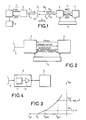
- a mobile station or badge 1 comprises a microwave part 3, an information processing part 4 and a power supply 5.
- the exchanges between these two parts relate to modulation-demodulation and transmission / reception commands.
- the fixed station or beacon 2 comprises a microwave source, a microwave part 6, an information processing part 7, and a computer 8 which makes it possible to manage all of the radioelectric exchanges carried out with the badges, via the antennas 9 for each badge and 10 for the tag or reader.
- modulations used in these systems are generally of the OOK type (in On-Off-Keying amplitude modulation), of the PSK type (in O / ⁇ Phase-Shift-Keying phase modulation), or FSK (Frequency Shift Keying).
- the operation of the modem is not the same depending on whether the tag interrogates the badge or whether the badge responds to the tag.
- the badge In the direction of interrogation of the badge 1 by the reader 2, the latter generates (P li ) a modulated microwave signal.
- the badge receives this signal (P br ) and demodulates it: it is a step which makes it possible to activate the badge which was in the standby state.
- the reader In the direction of the response from badge 1 to reader 2, the reader then generates an unmodulated microwave signal.
- the badge receives this signal, the module - that is to say the load of information about which it has been interrogated - and re-emits a signal comprising, as appropriate, either losses or gain.
- a high rate of information in turn requires that the modulation function of the modem be at low impedance, which moreover corresponds to higher energy consumption during the duration of the response from the badge to the reader.
- the badge in the standby state, transmits to its processing circuit 4 a series of information at low bit rates, which are identified by said circuit as an interrogation originating from the reader 2.
- the processing circuit 4 of the badge then "wakes up" the modem 3 by transmitting signals which act on means which modify the impedance or impedances of the modem, and allow it to respond with a high flow of information to the interrogation of the reader.
- the invention relates to a circuit for increasing the rate of information by microwave electromagnetic waves, in a data exchange system between a fixed station and a mobile station, called a portable badge, which includes a modem and an information processing circuit which is under high impedance and low consumption electric in the standby state, when the fixed station does not transmit a signal, this circuit being characterized in that, as soon as the fixed station transmits an interrogation signal with a low information rate (kilobits / sec), transmitted by the modem to the processing circuit, the latter emits a "wake-up" signal from the modem which acts on means reducing the modem's output impedance, thereby increasing the information rate (mega bits / sec) exchanged with the fixed station.
- a portable badge which includes a modem and an information processing circuit which is under high impedance and low consumption electric in the standby state, when the fixed station does not transmit a signal
- this circuit being characterized in that, as soon as the fixed station transmits an interrogation signal with a low information rate (
- FIG. 2 repeats the part of the badge 1 of FIG. 1, but shows a new link between the modem 3 and the information processing circuit 4.
- the transmission rates are generally limited in the direction from the reader to the badge. Indeed, although there is no particular problem for a reader to transmit at high speed, because its consumption does not matter, on the other hand if the badge demodulation function is unique, there is only one only energy state, this must be carried out at very high impedance, because it corresponds to the standby state under very low energy consumption - because of the "button" batteries which supply the badge.
- the time constants linked to the high impedances of the modem 3 and to the input capacities of the processing circuit 4, limit the demodulation rate to a few tens of kilobits / second.
- This low speed is sufficient to activate the information processing circuit 4, but insufficient to ensure data exchange between a reader and a plurality of badges: several megabits / second are necessary.
- the processing circuit 4 when the processing circuit 4 detects an interrogation coming from the reader 2, it sends to the modem 3 of the badge a signal which "wakes it up", and lowers its characteristic impedances, thus authorizing a high flow of information.
- the badge wake-up process is based on a change in the bias point of the transistor which functions as a detector in the modem 3.
- FIG. 3 gives the example of a field effect transistor, polarized on its gate at a voltage Vg sO close to the pinch voltage Vp: the transistor is in the standby state, and to this voltage V 9s0 corresponds a low drain current I ds , 2 ⁇ A for example.
- the gate bias voltage is switched to a higher value Vg s1 , to which corresponds a higher drain current I ds , for example between 10 and 100 ⁇ A, which decreases the impedances and time constants. If I ds goes from 2pA to 20pA the information rate is multiplied by 10.
- one (or more) amplifier 31 can be used, in series with the detector transistor 11, in the modem 3 , as shown in Figure 4: it is the amplifier which is "awakened", to transmit at high speed.
- the amplifier 31 works at the demodulation frequency, and its bias voltage is changed, while the transistor 11 continues to be in an optimal bias zone for the detection function.
- the basis of this arrangement consists in lowering the load impedance of the detector, therefore in increasing the information rate, without changing its point of polarization, and in compensating for the drop in level associated with the reduction in the output impedance by the change in polarization and therefore the increase in the gain of the amplifier 31 which follows the detector 11.
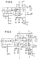
- FIG. 5 gives the detailed electrical diagram of a broadband modem, produced as an integrated circuit according to the invention, in which the polarization point of the transistor used as a detector is modified.
- the circuit shown is active in reception and passive in transmission, but other types of circuits can be adapted according to the invention.
- Capacities 15 and 22 are microwave decoupling capacities.
- Resistors 23 and 19 are of high values, of the order of 100 kn and 500 kn respectively. It is they which, in the standby state, polarize the drain and the source, and consequently determine Vg s and I ds .
- these two polarization resistors 23 and 19 are almost short-circuited by the two resistors 25 and 26, respectively, which are of the order of 10 k ⁇ , that is to say significantly lower in value than 100 and 500 k ⁇ .
- the switching between resistors 23 and 25, on the one hand, and 19 and 26, on the other hand, is carried out by means of transistors 27 and 28 respectively, when they are in the on state.
- These switching transistors 27 and 28 are controlled by the information processing circuit 4, by a signal applied to the wake-up terminal REV, and limited by the resistor 29.
- the resistor 30 sets the gates of the switching transistors 27 and 28 to -V, if these are not controlled or if the wake-up function is at high impedance: indeed, the high impedance state is often that of the logic gates d 'a processing circuit in "standby" mode. The transistors 27 and 28 are then blocked.
- the amplifier at the demodulation frequency essentially consists of at least one transistor 31, connected by means of a decoupling capacitor 32 to the load of the microwave transistor 11.
- the load LF of the transistor 11 is constituted by the resistance 23 (approximately 100 kn), the capacity 32 and the resistance 33 (approximately 500 k ⁇ - 1 M ⁇ ).
- Transistor 34 when controlled by the wake-up signal REV at the same time as transistors 27 and 28, switches the load LF of the detector transistor 11: its load resistance 33 (0.5 - -1 M ⁇ ) at 1 the standby state is shunted by the resistor 35 of low value (10 k ⁇ ) in the awakened state.
- the resistors 36 and 37 are stabilization resistors of the transistor 31 in the waking state: its drain load is constituted by the resistor 38 of high value (approximately 100 k ⁇ ) and the microwave decoupling capacity 39. Its source, decoupled by a capacitor 15, is self-polarized by a resistor 40 and a capacitor 41, in the same way as the source of the detector transistor 11: like the resistor 19, the resistor 40 has a high value, around 500 k ⁇ .
- FIG. 6 there is only one amplification stage, comprised between the lines AA and BB, between the detector stage and the wake-up stage by changing the polarization points. If the information rate requested from the badge must be higher than that supplied with a single amplification stage, there is no difficulty for those skilled in the art to cascade several amplification stages identical to that which is represented: it is only necessary to provide that each amplifier has its own wake-up stage, that is the transistors 27 and 28, and the associated circuits. The transistor 34, and its associated circuit 32 + 35, which switches the output impedance of the detector transistor 11, remains unique if there are several amplification stages. The demodulated DEM output is taken from the last amplifier.
- the two examples which have been exposed use a semi-active type modem.
- the invention is applicable to other types of modem, of which it suffices to change the polarization of the detector transistor.
- production in an integrated circuit does not limit the application of the invention, which can be carried out in a hybrid circuit, using microstrip lines which replace the inductors and the capacitors.
Landscapes
- Engineering & Computer Science (AREA)
- Radar, Positioning & Navigation (AREA)
- Remote Sensing (AREA)
- Physics & Mathematics (AREA)
- General Physics & Mathematics (AREA)
- Computer Networks & Wireless Communication (AREA)
- Artificial Intelligence (AREA)
- Computer Vision & Pattern Recognition (AREA)
- Theoretical Computer Science (AREA)
- Exchange Systems With Centralized Control (AREA)
- Radar Systems Or Details Thereof (AREA)
- Data Exchanges In Wide-Area Networks (AREA)
- Transceivers (AREA)
- Mobile Radio Communication Systems (AREA)
- Digital Transmission Methods That Use Modulated Carrier Waves (AREA)
Applications Claiming Priority (2)
| Application Number | Priority Date | Filing Date | Title |
|---|---|---|---|
| FR9014291 | 1990-11-16 | ||
| FR9014291A FR2669479B1 (fr) | 1990-11-16 | 1990-11-16 | Circuit d'augmentation du debit d'informations dans un systeme d'echange de donnees. |
Publications (2)
| Publication Number | Publication Date |
|---|---|
| EP0486366A1 true EP0486366A1 (de) | 1992-05-20 |
| EP0486366B1 EP0486366B1 (de) | 1995-03-22 |
Family
ID=9402272
Family Applications (1)
| Application Number | Title | Priority Date | Filing Date |
|---|---|---|---|
| EP91402990A Expired - Lifetime EP0486366B1 (de) | 1990-11-16 | 1991-11-07 | Schaltkreis zur Steigerung der Informationsabgabe in einem Datenaustauschsystem |
Country Status (8)
| Country | Link |
|---|---|
| US (1) | US5191345A (de) |
| EP (1) | EP0486366B1 (de) |
| JP (1) | JPH04286982A (de) |
| AT (1) | ATE120278T1 (de) |
| CA (1) | CA2055580A1 (de) |
| DE (1) | DE69108353T2 (de) |
| FR (1) | FR2669479B1 (de) |
| HK (1) | HK47597A (de) |
Cited By (2)
| Publication number | Priority date | Publication date | Assignee | Title |
|---|---|---|---|---|
| EP0578457A3 (en) * | 1992-07-06 | 1994-08-17 | Plessey Semiconductors Ltd | A data communication system |
| AU725500B2 (en) * | 1997-12-29 | 2000-10-12 | Samsung Electronics Co., Ltd. | Method and apparatus for controlling and maintaining a tower top low noise amplifier |
Families Citing this family (2)
| Publication number | Priority date | Publication date | Assignee | Title |
|---|---|---|---|---|
| DE4332475C2 (de) * | 1993-09-24 | 2002-12-05 | Bosch Gmbh Robert | Fahrzeuggerät zur Datenübertragung an eine ortsfeste Bake |
| US10402932B2 (en) * | 2017-04-17 | 2019-09-03 | Intel Corporation | Power-based and target-based graphics quality adjustment |
Citations (3)
| Publication number | Priority date | Publication date | Assignee | Title |
|---|---|---|---|---|
| AU558130B2 (en) * | 1981-01-21 | 1987-01-22 | Australian Meat and Livestock Corp., The | Interrogator/transponder |
| EP0245555A1 (de) * | 1986-03-31 | 1987-11-19 | Lo-Jack Corporation | Verfahren, System und Apparat zum Orten und/oder zum Verfolgen gestohlener oder vermisster Fahrzeuge und dgl. |
| EP0297688A1 (de) * | 1987-07-03 | 1989-01-04 | N.V. Nederlandsche Apparatenfabriek NEDAP | Elektronische Identifizierungsanordnung |
Family Cites Families (2)
| Publication number | Priority date | Publication date | Assignee | Title |
|---|---|---|---|---|
| NL162494C (nl) * | 1973-02-28 | 1980-05-16 | Philips Nv | Inrichting voor het identificeren van voertuigen. |
| US4656472A (en) * | 1985-01-23 | 1987-04-07 | Walton Charles A | Proximity identification system with power aided identifier |
-
1990
- 1990-11-16 FR FR9014291A patent/FR2669479B1/fr not_active Expired - Fee Related
-
1991
- 1991-11-07 DE DE69108353T patent/DE69108353T2/de not_active Expired - Fee Related
- 1991-11-07 AT AT91402990T patent/ATE120278T1/de active
- 1991-11-07 EP EP91402990A patent/EP0486366B1/de not_active Expired - Lifetime
- 1991-11-14 CA CA002055580A patent/CA2055580A1/fr not_active Abandoned
- 1991-11-15 US US07/793,095 patent/US5191345A/en not_active Expired - Fee Related
- 1991-11-16 JP JP3328193A patent/JPH04286982A/ja active Pending
-
1997
- 1997-04-10 HK HK47597A patent/HK47597A/xx not_active IP Right Cessation
Patent Citations (3)
| Publication number | Priority date | Publication date | Assignee | Title |
|---|---|---|---|---|
| AU558130B2 (en) * | 1981-01-21 | 1987-01-22 | Australian Meat and Livestock Corp., The | Interrogator/transponder |
| EP0245555A1 (de) * | 1986-03-31 | 1987-11-19 | Lo-Jack Corporation | Verfahren, System und Apparat zum Orten und/oder zum Verfolgen gestohlener oder vermisster Fahrzeuge und dgl. |
| EP0297688A1 (de) * | 1987-07-03 | 1989-01-04 | N.V. Nederlandsche Apparatenfabriek NEDAP | Elektronische Identifizierungsanordnung |
Cited By (2)
| Publication number | Priority date | Publication date | Assignee | Title |
|---|---|---|---|---|
| EP0578457A3 (en) * | 1992-07-06 | 1994-08-17 | Plessey Semiconductors Ltd | A data communication system |
| AU725500B2 (en) * | 1997-12-29 | 2000-10-12 | Samsung Electronics Co., Ltd. | Method and apparatus for controlling and maintaining a tower top low noise amplifier |
Also Published As
| Publication number | Publication date |
|---|---|
| DE69108353D1 (de) | 1995-04-27 |
| EP0486366B1 (de) | 1995-03-22 |
| DE69108353T2 (de) | 1995-07-20 |
| US5191345A (en) | 1993-03-02 |
| CA2055580A1 (fr) | 1992-05-17 |
| HK47597A (en) | 1997-04-18 |
| JPH04286982A (ja) | 1992-10-12 |
| FR2669479A1 (fr) | 1992-05-22 |
| FR2669479B1 (fr) | 1993-01-22 |
| ATE120278T1 (de) | 1995-04-15 |
Similar Documents
| Publication | Publication Date | Title |
|---|---|---|
| EP0486367B1 (de) | Modem für Mikrowellenkarte mit einem Reflexionsverstärker | |
| EP1045336A1 (de) | Enggekoppeltes Betriebsverfahren eines elektromagnetischen Transpondersystem | |
| EP0412884B1 (de) | Funksystem zur Datenübertragung an eine preiswerte passive Endstelle | |
| EP2230774B1 (de) | Verfahren zur Herstellung einer Datenverbindung zwischen zwei Prozessoren, insbesondere in einem NFC-Chipset | |
| EP0486364B1 (de) | Elektromagnetische Wellen nutzendes Datenaustauschsystem | |
| EP1445877B1 (de) | Kommunikation zwischen elektromagnetischen Transpondern | |
| EP0903949A1 (de) | Verfahren zur Initialisierung einer Verbindung zwischen einer Mobilstation und einer Haushaltsbasisstation | |
| JP2003503903A (ja) | 負性インピーダンス増幅器を備えた反射変調器回路 | |
| FR2624677A1 (fr) | Systeme de liaison hertzienne bidirectionnelle | |
| EP0449720B1 (de) | Zweirichtstrahlübertragungsaktivantenne | |
| EP0486365B1 (de) | Vorrichtung für Telekommunikationen durch elektromagnetische Wellen | |
| EP0486366B1 (de) | Schaltkreis zur Steigerung der Informationsabgabe in einem Datenaustauschsystem | |
| EP3012980A1 (de) | Verfahren zur steuerung des betriebs, insbesondere der belastungsmodulation, eines objekts, das in der lage ist, kontaktlos mit einem lesegerät zu kommunizieren, entsprechende vorrichtung und entsprechendes objekt | |
| FR2618907A1 (fr) | Systeme d'identification a balise repondeuse sans source d'alimentation | |
| WO2013186478A1 (fr) | Gestion d'energie dans un transpondeur electromagnetique | |
| EP0639486B1 (de) | Alarmsystem für eine mobile Funkstation | |
| EP1181769A2 (de) | Vorrichtung zur demodulation eines am-signals | |
| WO2004064257A2 (fr) | Procede de communication entre un emetteur d'ordres et un emetteur-recepteur d'ordres | |
| EP0671702A1 (de) | Mikrowellen-Nahbereich-Identifizierungssystem | |
| EP1435062A1 (de) | Modulator für elektromagnetische signale ausgesandt von einem kontaktlosen sender/empfänger-system | |
| EP0533584A1 (de) | Drahtlose Information-Sende- und Empfangseinrichtung und Datenaustauschsystem mit einer solchen Vorrichtung | |
| WO2000065795A1 (fr) | Procede et dispositif de transmission de donnees par signaux sonores |
Legal Events
| Date | Code | Title | Description |
|---|---|---|---|
| PUAI | Public reference made under article 153(3) epc to a published international application that has entered the european phase |
Free format text: ORIGINAL CODE: 0009012 |
|
| AK | Designated contracting states |
Kind code of ref document: A1 Designated state(s): AT BE CH DE ES GB GR IT LI LU NL SE |
|
| 17P | Request for examination filed |
Effective date: 19920624 |
|
| 17Q | First examination report despatched |
Effective date: 19940302 |
|
| RAP1 | Party data changed (applicant data changed or rights of an application transferred) |
Owner name: THOMSON-CSF SEMICONDUCTEURS SPECIFIQUES |
|
| GRAA | (expected) grant |
Free format text: ORIGINAL CODE: 0009210 |
|
| AK | Designated contracting states |
Kind code of ref document: B1 Designated state(s): AT BE CH DE ES GB GR IT LI LU NL SE |
|
| PG25 | Lapsed in a contracting state [announced via postgrant information from national office to epo] |
Ref country code: GR Free format text: LAPSE BECAUSE OF FAILURE TO SUBMIT A TRANSLATION OF THE DESCRIPTION OR TO PAY THE FEE WITHIN THE PRESCRIBED TIME-LIMIT Effective date: 19950322 Ref country code: ES Free format text: THE PATENT HAS BEEN ANNULLED BY A DECISION OF A NATIONAL AUTHORITY Effective date: 19950322 |
|
| REF | Corresponds to: |
Ref document number: 120278 Country of ref document: AT Date of ref document: 19950415 Kind code of ref document: T |
|
| ITF | It: translation for a ep patent filed | ||
| REF | Corresponds to: |
Ref document number: 69108353 Country of ref document: DE Date of ref document: 19950427 |
|
| GBT | Gb: translation of ep patent filed (gb section 77(6)(a)/1977) |
Effective date: 19950526 |
|
| RAP2 | Party data changed (patent owner data changed or rights of a patent transferred) |
Owner name: THOMSON-CSF SEMICONDUCTEURS SPECIFIQUES |
|
| NLT2 | Nl: modifications (of names), taken from the european patent patent bulletin |
Owner name: THOMSON-CSF SEMICONDUCTEURS SPECIFIQUES |
|
| PG25 | Lapsed in a contracting state [announced via postgrant information from national office to epo] |
Ref country code: LU Free format text: LAPSE BECAUSE OF NON-PAYMENT OF DUE FEES Effective date: 19951130 Ref country code: LI Effective date: 19951130 Ref country code: CH Effective date: 19951130 Ref country code: BE Effective date: 19951130 |
|
| PLBE | No opposition filed within time limit |
Free format text: ORIGINAL CODE: 0009261 |
|
| STAA | Information on the status of an ep patent application or granted ep patent |
Free format text: STATUS: NO OPPOSITION FILED WITHIN TIME LIMIT |
|
| 26N | No opposition filed | ||
| BERE | Be: lapsed |
Owner name: THOMSON-CSF SEMICONDUCTEURS SPECIFIQUES Effective date: 19951130 |
|
| REG | Reference to a national code |
Ref country code: CH Ref legal event code: PL |
|
| PGFP | Annual fee paid to national office [announced via postgrant information from national office to epo] |
Ref country code: NL Payment date: 19991013 Year of fee payment: 9 |
|
| PGFP | Annual fee paid to national office [announced via postgrant information from national office to epo] |
Ref country code: GB Payment date: 19991014 Year of fee payment: 9 |
|
| PGFP | Annual fee paid to national office [announced via postgrant information from national office to epo] |
Ref country code: SE Payment date: 19991015 Year of fee payment: 9 Ref country code: DE Payment date: 19991015 Year of fee payment: 9 |
|
| PGFP | Annual fee paid to national office [announced via postgrant information from national office to epo] |
Ref country code: AT Payment date: 19991129 Year of fee payment: 9 |
|
| PG25 | Lapsed in a contracting state [announced via postgrant information from national office to epo] |
Ref country code: GB Free format text: LAPSE BECAUSE OF NON-PAYMENT OF DUE FEES Effective date: 20001107 Ref country code: AT Free format text: LAPSE BECAUSE OF NON-PAYMENT OF DUE FEES Effective date: 20001107 |
|
| PG25 | Lapsed in a contracting state [announced via postgrant information from national office to epo] |
Ref country code: SE Free format text: THE PATENT HAS BEEN ANNULLED BY A DECISION OF A NATIONAL AUTHORITY Effective date: 20001129 |
|
| PG25 | Lapsed in a contracting state [announced via postgrant information from national office to epo] |
Ref country code: NL Free format text: LAPSE BECAUSE OF NON-PAYMENT OF DUE FEES Effective date: 20010601 |
|
| GBPC | Gb: european patent ceased through non-payment of renewal fee |
Effective date: 20001107 |
|
| EUG | Se: european patent has lapsed |
Ref document number: 91402990.5 |
|
| NLV4 | Nl: lapsed or anulled due to non-payment of the annual fee |
Effective date: 20010601 |
|
| PG25 | Lapsed in a contracting state [announced via postgrant information from national office to epo] |
Ref country code: DE Free format text: LAPSE BECAUSE OF NON-PAYMENT OF DUE FEES Effective date: 20010801 |
|
| PG25 | Lapsed in a contracting state [announced via postgrant information from national office to epo] |
Ref country code: IT Free format text: LAPSE BECAUSE OF NON-PAYMENT OF DUE FEES;WARNING: LAPSES OF ITALIAN PATENTS WITH EFFECTIVE DATE BEFORE 2007 MAY HAVE OCCURRED AT ANY TIME BEFORE 2007. THE CORRECT EFFECTIVE DATE MAY BE DIFFERENT FROM THE ONE RECORDED. Effective date: 20051107 |