EP0486827A2 - Matériau diélectrique et condensateur formé à partir de celui-ci - Google Patents
Matériau diélectrique et condensateur formé à partir de celui-ci Download PDFInfo
- Publication number
- EP0486827A2 EP0486827A2 EP91117979A EP91117979A EP0486827A2 EP 0486827 A2 EP0486827 A2 EP 0486827A2 EP 91117979 A EP91117979 A EP 91117979A EP 91117979 A EP91117979 A EP 91117979A EP 0486827 A2 EP0486827 A2 EP 0486827A2
- Authority
- EP
- European Patent Office
- Prior art keywords
- dielectric
- dielectric material
- oxides
- copper
- condenser
- Prior art date
- Legal status (The legal status is an assumption and is not a legal conclusion. Google has not performed a legal analysis and makes no representation as to the accuracy of the status listed.)
- Granted
Links
Images
Classifications
-
- H—ELECTRICITY
- H01—ELECTRIC ELEMENTS
- H01G—CAPACITORS; CAPACITORS, RECTIFIERS, DETECTORS, SWITCHING DEVICES, LIGHT-SENSITIVE OR TEMPERATURE-SENSITIVE DEVICES OF THE ELECTROLYTIC TYPE
- H01G4/00—Fixed capacitors; Processes of their manufacture
- H01G4/002—Details
- H01G4/018—Dielectrics
- H01G4/06—Solid dielectrics
- H01G4/08—Inorganic dielectrics
- H01G4/12—Ceramic dielectrics
- H01G4/1209—Ceramic dielectrics characterised by the ceramic dielectric material
- H01G4/1254—Ceramic dielectrics characterised by the ceramic dielectric material based on niobium or tungsteen, tantalum oxides or niobates, tantalates
- H01G4/1263—Ceramic dielectrics characterised by the ceramic dielectric material based on niobium or tungsteen, tantalum oxides or niobates, tantalates containing also zirconium oxides or zirconates
-
- C—CHEMISTRY; METALLURGY
- C04—CEMENTS; CONCRETE; ARTIFICIAL STONE; CERAMICS; REFRACTORIES
- C04B—LIME, MAGNESIA; SLAG; CEMENTS; COMPOSITIONS THEREOF, e.g. MORTARS, CONCRETE OR LIKE BUILDING MATERIALS; ARTIFICIAL STONE; CERAMICS; REFRACTORIES; TREATMENT OF NATURAL STONE
- C04B35/00—Shaped ceramic products characterised by their composition; Ceramics compositions; Processing powders of inorganic compounds preparatory to the manufacturing of ceramic products
- C04B35/01—Shaped ceramic products characterised by their composition; Ceramics compositions; Processing powders of inorganic compounds preparatory to the manufacturing of ceramic products based on oxide ceramics
- C04B35/48—Shaped ceramic products characterised by their composition; Ceramics compositions; Processing powders of inorganic compounds preparatory to the manufacturing of ceramic products based on oxide ceramics based on zirconium or hafnium oxides, zirconates, zircon or hafnates
- C04B35/49—Shaped ceramic products characterised by their composition; Ceramics compositions; Processing powders of inorganic compounds preparatory to the manufacturing of ceramic products based on oxide ceramics based on zirconium or hafnium oxides, zirconates, zircon or hafnates containing also titanium oxides or titanates
- C04B35/491—Shaped ceramic products characterised by their composition; Ceramics compositions; Processing powders of inorganic compounds preparatory to the manufacturing of ceramic products based on oxide ceramics based on zirconium or hafnium oxides, zirconates, zircon or hafnates containing also titanium oxides or titanates based on lead zirconates and lead titanates, e.g. PZT
- C04B35/493—Shaped ceramic products characterised by their composition; Ceramics compositions; Processing powders of inorganic compounds preparatory to the manufacturing of ceramic products based on oxide ceramics based on zirconium or hafnium oxides, zirconates, zircon or hafnates containing also titanium oxides or titanates based on lead zirconates and lead titanates, e.g. PZT containing also other lead compounds
-
- C—CHEMISTRY; METALLURGY
- C04—CEMENTS; CONCRETE; ARTIFICIAL STONE; CERAMICS; REFRACTORIES
- C04B—LIME, MAGNESIA; SLAG; CEMENTS; COMPOSITIONS THEREOF, e.g. MORTARS, CONCRETE OR LIKE BUILDING MATERIALS; ARTIFICIAL STONE; CERAMICS; REFRACTORIES; TREATMENT OF NATURAL STONE
- C04B35/00—Shaped ceramic products characterised by their composition; Ceramics compositions; Processing powders of inorganic compounds preparatory to the manufacturing of ceramic products
- C04B35/01—Shaped ceramic products characterised by their composition; Ceramics compositions; Processing powders of inorganic compounds preparatory to the manufacturing of ceramic products based on oxide ceramics
- C04B35/495—Shaped ceramic products characterised by their composition; Ceramics compositions; Processing powders of inorganic compounds preparatory to the manufacturing of ceramic products based on oxide ceramics based on vanadium, niobium, tantalum, molybdenum or tungsten oxides or solid solutions thereof with other oxides, e.g. vanadates, niobates, tantalates, molybdates or tungstates
- C04B35/497—Shaped ceramic products characterised by their composition; Ceramics compositions; Processing powders of inorganic compounds preparatory to the manufacturing of ceramic products based on oxide ceramics based on vanadium, niobium, tantalum, molybdenum or tungsten oxides or solid solutions thereof with other oxides, e.g. vanadates, niobates, tantalates, molybdates or tungstates based on solid solutions with lead oxides
- C04B35/499—Shaped ceramic products characterised by their composition; Ceramics compositions; Processing powders of inorganic compounds preparatory to the manufacturing of ceramic products based on oxide ceramics based on vanadium, niobium, tantalum, molybdenum or tungsten oxides or solid solutions thereof with other oxides, e.g. vanadates, niobates, tantalates, molybdates or tungstates based on solid solutions with lead oxides containing also titanates
-
- H—ELECTRICITY
- H01—ELECTRIC ELEMENTS
- H01G—CAPACITORS; CAPACITORS, RECTIFIERS, DETECTORS, SWITCHING DEVICES, LIGHT-SENSITIVE OR TEMPERATURE-SENSITIVE DEVICES OF THE ELECTROLYTIC TYPE
- H01G4/00—Fixed capacitors; Processes of their manufacture
- H01G4/002—Details
- H01G4/018—Dielectrics
- H01G4/06—Solid dielectrics
- H01G4/08—Inorganic dielectrics
- H01G4/12—Ceramic dielectrics
- H01G4/1209—Ceramic dielectrics characterised by the ceramic dielectric material
- H01G4/1236—Ceramic dielectrics characterised by the ceramic dielectric material based on zirconium oxides or zirconates
- H01G4/1245—Ceramic dielectrics characterised by the ceramic dielectric material based on zirconium oxides or zirconates containing also titanates
Definitions
- the present invention relates to a dielectric material that can be baked at low temperatures for a short period of time, and a condenser made from the dielectric material, thereby having excellent temperature characteristics, such as a dielectric constant varying within 10% of the base value measured at 20°C in the temperature range of -25°C to 85°C.
- Ceramic condensers are comprised of a dielectric material and electrodes placed on both sides of the dielectric material.
- the dielectric material requires, as one of electric properties the temperature dependence of its dielectric constant which is defined by JIS, etc.
- Examples of the dielectric materials having excellent temperature characteristics of dielectric constant include barium titanate materials which are used for conventional ceramic condensers.
- Electrode materials that can be used at such high temperatures during the baking process include only noble metals which have relatively high melting points, for example platinum, palladium, etc. The use of these expensive noble metals leads to the increase of the ceramic condenser prices.
- the proposed dielectric materials are ones made of perovskite type materials containing lead ion as a base, which have not only low baking temperatures, but provide excellent temperature characteristics of dielectric constant. Since these dielectric materials are sintered at these low temperatures, less expensive electrode materials having lower melting points, e.g., silver-palladium alloy can be used. Therefore, using these dielectric materials, and the electrode materials, ceramic condensers can be made at a lower cost.
- a thick-film condenser has been demanded as a ceramic condenser instead of a conventional chip condenser as the number of circuits placed on a single plate is increased.
- the thick-film condenser structurally requires a dielectric material that can be baked not only at low temperatures, but for a short period of time. Therefore, a dielectric material that can be used for such a thick-film condenser with flat temperature characteristics will be increasingly required.
- the aforementioned perovskite type dielectric material must be sintered in an atmosphere of low partial oxygen pressure so as to avoid oxidation and also be maintained at a temperature of 1000°C or higher for several hours so as to obtain a solid sintered body with a high dielectric constant.
- the dielectric material cannot be sufficiently sintered because a low-temperature and short-time sintering process is required for a thick-film condenser, thus failing in obtaining a desired characteristic of the condenser. If it is intended to sinter the dielectric material completely, the sintering temperature must be 1000°C or higher.
- electrode materials may be oxidized, and therefore, the above-mentioned silver-palladium alloy, or copper that has a further lower melting point, cannot be used, thus preventing the manufacture of ceramic condensers at a lower cost.
- the objective of this invention is to provide a dielectric material which has the flat temperature characteristics of dielectric constant and is able to be sintered at a low temperature of 1000°C or lower in a short period of time.
- the another objective of this invention is to provide an inexpensive condenser using such a dielectric material.
- the dielectric material of this invention which overcomes the above-discussed and numerous other disadvantages and deficiencies of the prior art, comprises a dielectric porcelain composition represented by the following general formula in the form of a prebaked powder, and 1.0-25.0 mole % of lead oxides in which the amounts of the lead oxides are converted into the amount of PbO: (1-x)[Pb(Mg 1/3 Nb 2/3 )CU a O 3+a ] xBa(Ti 1-b Zr b )O3 wherein, x, a and b values satisfy O.30 ⁇ x ⁇ 0.80, 0 ⁇ a ⁇ 0.30, and 0 ⁇ b ⁇ 0.15.
- the dielectric porcelain composition is a mixture of the solid solution of BaTiO3 and BaZrO3 to Pb(Mg 1/3 Nb 2/3 )Cu a O 3+a .
- the lead oxide is PbO, Pb3O4, or PbO2.
- Another dielectric material of this invention comprises a dielectric porcelain composition represented by the following general formula in the form of a pre-baked powder, and 1.0-25.0 mole % of lead oxides, and 1.0-15.0 mole % of copper oxides in which the amounts of the lead oxides, and the copper oxides are converted into those of PbO, and CuO, respectively: (1-x)[Pb(Mg 1/3 Nb 2/3 )Cu a O 3+a ] xBa(Ti 1-b Zr b )O3 wherein, x, a and b values satisfy 0.30 ⁇ x ⁇ 0.80, 0 ⁇ a ⁇ 0.25, and 0 ⁇ b ⁇ 0.15.
- the dielectric porcelain composition is a mixture of the solid solution of BaTiO3 and BaZrO3 to Pb(Mg 1/3 Nb 2/3 )Cu a O 3+a .
- the lead oxide is PbO, Pb3O4, or PbO2.
- the copper oxide is Cu2O or CuO.
- the condenser of this invention comprises a dielectric layer, and electrodes placed on both sides of the dielectric layer, wherein the dielectric layer consists essentially of a dielectric material comprising a dielectric porcelain composition represented by the following general formula in the form of a pre-baked powder, and 1.0-25.0 mole % of lead oxides in which the amounts of the lead oxides are converted into the amount of PbO: (1-x)[Pb(Mg 1/3 Nb 2/3 )Cu a O 3+a ] xBa(Ti 1-b Zr b )O3 wherein, x, a and b values satisfy 0.30 ⁇ x ⁇ 0.80, 0 ⁇ a ⁇ 0.30, and 0 ⁇ b ⁇ 0.15.
- the electrode is made from copper, silver, or silver-palladium alloy.
- Another condenser of this invention comprises a dielectric layer, and electrodes placed on both sides of the dielectric layer, wherein the dielectric layer consists essentially of a dielectric material comprising a dielectric porcelain composition represented by the following general formula in the form of a pre-baked powder, and 1.0-25.0 mole % of lead oxides, and 1.0-15.0 mole % of copper oxides in which the amounts of the lead oxides, and the copper oxides are converted into those of PbO, and CuO, respectively: (1-x)[Pb(Mg 1/3 Nbx 2/3 )Cu a O 3+a ] xBa(Ti 1-b Zr b )O3 wherein, x, a and b values satisfy 0.30 ⁇ x ⁇ 0.80, 0 ⁇ a ⁇ 0.25, and 0 ⁇ b ⁇ 0.15.
- the electrode is made from copper, silver, or silver-palladium alloy.
- Another condenser of this invention comprises a ceramic base plate, a lower electrode, a dielectric layer, and an upper electrode, wherein the lower electrode, the dielectric layer, and the upper electrode are laminated in this order on the ceramic base plate, wherein the dielectric layer consists essentially of a dielectric material comprising a dielectric porcelain composition represented by the following general formula in the form of a pre-baked powder, and 1.0-25.0 mole % of lead oxides in which the amounts of the lead oxides are converted into the amount of PbO: (1-x)[Pb(Mg 1/3 Nb 2/3 )Cu a O 3+a ] xBa(Ti 1-b Zr b )O3 wherein, x, a and b values satisfy 0.30 ⁇ x ⁇ 0.80, 0 ⁇ a ⁇ 0.30, and 0 ⁇ b ⁇ 0.15.
- the electrode is made from copper, silver, or silver-palladium alloy.
- Another condenser of this invention comprises a ceramic base plate, a lower electrode, a dielectric layer, and an upper electrode, wherein the lower electrode, the dielectric layer, and the upper electrode are laminated in this order on the ceramic base plate, wherein the dielectric layer consists essentially of a dielectric material comprising a dielectric porcelain composition represented by the following general formula in the form of a pre-baked powder, and 1.0-25.0 mole % of lead oxides, and 1.0-15.0 mole % of copper oxides in which the amounts of the lead oxides, and the copper oxides are converted into those of PbO, and CuO, respectively: (1-x)[Pb(Mg 1/3 Nb 2/3 )Cu a O 3+a ] xBa(Ti 1-b Zr b )O3 wherein, x, a and b values satisfy 0.30 ⁇ x ⁇ 0.80, 0 ⁇ a ⁇ 0.25, and 0 ⁇ b ⁇ 0.15.
- the electrode is made from copper, silver, or silver-palladium alloy.
- the invention described herein makes possible the objectives of (1) providing a dielectric material that can be baked at low temperatures of 1000°C or less for a short period of time; and (2) providing a condenser which is made from the dielectric material, and has excellent temperature characteristics, i.e., stable dielectric characteristics at different temperatures, for example a dielectric constant varying within 10% of the base value measured at 20°C in the temperature range of -25°C to 85°C.
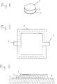
- Figure 1 is a perspective view of the ceramic condenser illustrating one embodiment of this invention.
- Figure 2 is a top plan view of the thick-film condenser illustrating one embodiment of this invention.
- Figure 3 is a side cross-sectional view of the thick-film condenser illustrating one embodiment of this invention.
- a Pb(Mg 1/3 Nb 2/3 )Cu a O 3+a (hereinafter referred to as PMN) powder is prepared by pre-baking the combination of the prescribed amounts of MgO and Nb2O5 at 950°C for 5 hours in the atmosphere to obtain MgNb2O6, grinding the MgNb2O6 by a ball mill, then pre-baking the combination of the prescribed amounts of the ground MgNb2O6, PbO and CuO at 900°C for 2 hours in the atmosphere, and grinding the combination by a ball mill.
- BTZ a solid solution of BaTiO3 and BaZrO3 (hereinafter referred to as BTZ) is prepared by pre-baking the combination of the prescribed amounts of BaCO3, TiO2 and ZrO2 at 1300°C for 2 hours in the atmosphere, and then grinding the combination by a ball mill.
- the prescribed amounts of the resulting PMN powder, and BTZ powder are wet-blended by a ball mill, and dried.
- the dried mixture is pre-baked at 800°C for 2 hours in the atmosphere, ground by a ball mill, and dried.
- PbO and CuO are added as sub-components with mixing by a mixing and grinding machine.
- 6 wt% polyvinylalcohol solution is added as a binder in the amount of 6 wt% of the mixture, and granulated by a 32 mesh sieve.
- the final mixture is molded under a pressure of 1000 kg/cm2 in the form of a disk having about 13 mm diameter, and about 5 mm thickness. Then, the molding is allowed to stand at 600°C for 1 hour in the atmosphere to remove the binder, and baked at 900°C for 10 minutes under a nitrogen atmosphere.
- the baked molding is worked into a disk having 1 mm thickness, coated with an Ag paste on both sides as electrodes, and dried at 120°C in the atmosphere to form a single-plate condenser as shown in Figure 1.
- the condenser comprises of electrodes 1, 1', and a dielectric Layer 2 as shown in Figure 1.
- Table 1 illustrates the composition of the major components and the sub-components contained in the dielectric materials of this example.
- Table 2 illustrates the dielectric characteristics of the single-plate condenser, i.e., dielectric constant, tan ⁇ (dielectric loss factor), and insulation resistance, and temperature variation percentage of the dielectric constant (a value measured at 20°C is the base value).
- the dielectric constant, and tan ⁇ (dielectric loss factor) are measured under an electric field of 1 kHz and 1 V/mm. Also, the dielectric resistance is measured one minute after a 30 V is applied. Table 2 Sample No.
- Dielectric characteristic Temperature variation percentage of the dielectric constant (%) Dielectric constant tan ⁇ (%) Insulation resistance 1012 ⁇ cm -25°C -85°C 1 # 1100 4.5 0.06 -14.2 -16.3 2 520 2.0 1.15 -8.3 -6.2 3 1680 2.1 1.02 -8.1 -5.9 4 1120 2.2 0.94 -9.1 -6.1 5 # 220 3.8 0.87 -11.0 -9.8 6 570 1.8 1.70 -7.5 -2.5 7 1900 2.1 1.53 -7.5 -6.8 8 1520 2.3 1.17 -9.3 -8.0 9 480 1.7 1.98 -8.0 -2.1 10 1850 1.9 2.04 -8.2 -2.5 11 1560 2.2 1.82 -9.6 -3.4 12 # 1200 3.1 0.07 -7.5 -12.0 13 # 1450 2.5 1.30 -5.3 -12.3 14 # 1500 7.4 0.04 -10.1 -11.5 15 420 1.6 1.14 -8.9 -5.2 16 1330 1.8 1.22
- the dielectric materials of this invention are sintered sufficiently, and have a lower temperature variation percentage, i.e., a dielectric constant varying within 10% of the base value measured at 20°C in the temperature range of -25°C to 85°C, and a high enough insulation resistance for practical uses even though it is baked at a low temperature of 900°C for a short period of time.
- the dielectric materials have improved temperature characteristics in high temperature areas because a suitable amount of Zr atom contained therein reduces its Curie point.
- control sample No. 5 is not sintered sufficiently at 900°C because of the lower amounts of PbO and CuO, i.e., the absence of PbO or CuO as the sub-component, and therefore provides an unacceptably lower dielectric constant.
- control sample No. 12 containing the excess amounts of PbO and CuO is sintered sufficiently, it has unsatisfactory temperature characteristics of dielectric constant, i.e., a higher temperature variation percentage, and increased dielectric loss which is not acceptable for practical uses.
- control sample No. 1 control sample No.
- control sample No. 21 containing a large amount of BTZ is neither sintered sufficiently, nor provides excellent characteristics derived from PMN. Also, control sample No. 20 which contains a large amount of Zr does not provide good temperature characteristics because of severely reduced Curie point. Moreover, control sample No. 14 is not acceptable because of low dielectric loss factor derived from the excess amount of Cu contained in PMN.
- Single-plate condensers are made by the same procedure as in Example 1 except that the powder mixture is prepared by adding as the sub-components the prescribed amounts of Pb3O4, PbO2 and Cu2O to the dielectric porcelain composition represented by the following formula: 0.60[Pb(Mg 1/3 Nb 2/3 )Cu 0.1 O 3.1 ] 0.40Ba(Ti 0.9 Zr 0.1 )O3
- the dielectric characteristics of the single-plate condensers i.e., dielectric constant, dielectric loss factor, insulation resistance, and temperature variation percentage of the dielectric constant (a value measured at 20°C is the base value) are also measured in the same manner.
- Table 3 illustrates the amounts added of Pb3O4, PbO2 and Cu2O.
- Table 4 illustrates the dielectric characteristics, i.e., dielectric constant, tan ⁇ (dielectric loss factor), and insulation resistance, and temperature variation percentage of the dielectric constant. Table 3 Sample No.
- the dielectric materials of this invention are sintered sufficiently, and have a lower temperature variation percentage, i.e., a dielectric constant varying within 10% of the base value measured at 20°C in the temperature range of -25°C to 85°C, and a high enough insulation resistance for practical uses even though it is baked at a low temperature of 900°C for a short period of time.
- Example 2 To the dielectric composition of major components which is pre-baked and dried by the same procedure as in Example 1, there are added the prescribed amounts of PbO and CuO with wet-blending by a ball mill, and then dried. Then, a vehicle of a resin which contains ethyl cellulose as a major component dissolved in a solvent is added to the mixture of major component and sub-component, and kneaded by a three-stage roll to prepare a dielectric paste.
- a vehicle of a resin which contains ethyl cellulose as a major component dissolved in a solvent is added to the mixture of major component and sub-component, and kneaded by a three-stage roll to prepare a dielectric paste.
- copper paste is coated as a lower electrode 3 on an alumina base plate 4 having 96% purity, and dried as shown in Figures 2 and 3. Then, the aforementioned dielectric paste is coated in a 50-60 ⁇ m thickness on the lower electrode 3, and dried to form a dielectric layer 2. Moreover, the same copper paste as used for the lower electrode 3, is coated as an upper electrode 1 on the dielectric layer 2 and dried to form a thick film having a laminated structure of three layers, i.e., electrode - dielectric layer - electrode. The thick film is baked in a belt furnace at 800-1000°C for 5-30 minutes under a nitrogen atmosphere to form a thick-film condenser.
- the dielectric characteristics of the thick-film condenser i.e., dielectric constant, tan ⁇ (dielectric loss factor), and insulation resistance, and temperature variation percentage of the dielectric constant are measured.
- the dielectric constant, and tan ⁇ (dielectric loss factor) are measured under electric field of 1 kHz and 1 V/mm. Also, the dielectric resistance is measured one minute after 30 V is applied.
- Table 5 illustrates the composition of the major components and the sub-components used in the dielectric materials.
- Table 6 illustrates the dielectric characteristics, i.e., dielectric constant, tan ⁇ (dielectric loss factor), and insulation resistance, and temperature variation percentage of the dielectric constant (a value measured at 20°C is the base value) of the thick-film condenser prepared by baking at 900°C for 10 minutes under a nitrogen atmosphere.
- the dielectric materials of this invention is sintered sufficiently, and have a lower temperature variation percentage, i.e., a dielectric constant varying within 10% of the value measured at 20°C in the temperature range of -25°C to 85°C, and a high enough insulation resistance, enough for practical uses even though it is baked at a low temperature of 900°C for a short period of time.
- the dielectric material has improved temperature characteristics in high temperature areas because of the suitable amount of Zr atoms contained therein reduces its Curie point.
- control sample No. 5 is not sintered sufficiently at 900°C because of the lower amounts of PbO and CuO, i.e., the absence of PbO or CuO as the sub-component, and therefore provides an unacceptably lower dielectric constant.
- control sample No. 12 containing the excess amounts of PbO and CuO is sintered sufficiently, it has unsatisfactory temperature characteristics of dielectric constant, i.e., a higher temperature variation percentage and increased dielectric loss which is not acceptable for practical uses.
- control sample No. 1 when a small amount of BTZ is added (control sample No. 1), the dielectric constant of the resulting dielectric material has higher temperature dependence derived from PMN.
- control sample No. 1 when a small amount of BTZ is added (control sample No. 1), the dielectric constant of the resulting dielectric material has higher temperature dependence derived from PMN.
- control sample No. 1 when a small amount of BTZ is added (control sample No. 1), the dielectric constant of the resulting dielectric material has higher temperature dependence
- control sample No. 21 containing a large amount of BTZ is neither sintered sufficiently, nor provides excellent characteristics derived from PMN. Also, control sample No. 20 which contains a large amount of Zr does not provide good temperature characteristics because of a severely reduced Curie point. Moreover, control sample No. 14 is not acceptable because of a low dielectric loss factor derived from the excess amount of Cu contained in the PMN.
- Thick-film condensers are made by the same procedure as in Example 3 except that the powder mixture is prepared by adding the prescribed amounts of Pb3O4, PbO2 and Cu2O to the dielectric composition represented by the following formula: 0.60[Pb(Mg 1/3 Nb 2/3 )Cu 0.1 O 3.1 ] 0.40Ba(Ti 0.9 Zr 0.1 )O3
- the dielectric characteristics of the thick-film condensers i.e., dielectric constant tan ⁇ , dielectric loss factor, insulation resistance, and temperature variation percentage of the dielectric constant are also measured in the same manner.
- Table 7 illustrates the amounts added of Pb3O4, PbO2 and Cu2O.
- Table 8 illustrates the dielectric characteristics, i.e., dielectric constant, tan ⁇ (dielectric loss factor), and insulation resistance, and temperature variation percentage of the dielectric constant.
- the dielectric materials of this invention are sintered sufficiently, and have a lower temperature variation percentage, i.e., a dielectric constant varying within 10% of the base value measured at 20°C in the temperature range of -25°C to 85°C, and a high enough insulation resistance for practical uses even though it is baked at a low temperature of 900°C for a short period of time.
- Pb3O4 or PbO2 is used as the sub-component in the dielectric composition, better dielectric characteristics are obtained than using PbO, because Pb3O4 and PbO2 are decomposed into PbO and oxygen which aids in removing the resin components at baking temperatures.
- the electrode materials that can be used for the condenser of this invention include those available at the baking temperature of the dielectric material, i.e., 800-1000°C, for example, copper, silver, and silver-palladium alloy, and the like. The use of these electrode materials provides less expensive condensers.
- the dielectric materials are baked under a nitrogen atmosphere in these examples, they may be baked in the atmosphere.
Landscapes
- Engineering & Computer Science (AREA)
- Chemical & Material Sciences (AREA)
- Ceramic Engineering (AREA)
- Manufacturing & Machinery (AREA)
- Power Engineering (AREA)
- Organic Chemistry (AREA)
- Structural Engineering (AREA)
- Inorganic Chemistry (AREA)
- Materials Engineering (AREA)
- Microelectronics & Electronic Packaging (AREA)
- Composite Materials (AREA)
- Inorganic Insulating Materials (AREA)
- Compositions Of Oxide Ceramics (AREA)
- Ceramic Capacitors (AREA)
Applications Claiming Priority (2)
| Application Number | Priority Date | Filing Date | Title |
|---|---|---|---|
| JP2317341A JPH04188504A (ja) | 1990-11-20 | 1990-11-20 | 誘電体磁器組成物 |
| JP317341/90 | 1990-11-20 |
Publications (3)
| Publication Number | Publication Date |
|---|---|
| EP0486827A2 true EP0486827A2 (fr) | 1992-05-27 |
| EP0486827A3 EP0486827A3 (en) | 1992-12-09 |
| EP0486827B1 EP0486827B1 (fr) | 1995-05-31 |
Family
ID=18087141
Family Applications (1)
| Application Number | Title | Priority Date | Filing Date |
|---|---|---|---|
| EP91117979A Expired - Lifetime EP0486827B1 (fr) | 1990-11-20 | 1991-10-22 | Matériau diélectrique et condensateur formé à partir de celui-ci |
Country Status (4)
| Country | Link |
|---|---|
| US (1) | US5183786A (fr) |
| EP (1) | EP0486827B1 (fr) |
| JP (1) | JPH04188504A (fr) |
| DE (1) | DE69110108T2 (fr) |
Cited By (2)
| Publication number | Priority date | Publication date | Assignee | Title |
|---|---|---|---|---|
| GB2353994A (en) * | 1999-09-11 | 2001-03-14 | Univ Cranfield | Sintering aid for ceramics |
| EP1135783A4 (fr) * | 1998-10-02 | 2004-05-12 | Sarnoff Corp | Condensateurs noyes a constante dielectrique elevee a capacite couplee |
Families Citing this family (3)
| Publication number | Priority date | Publication date | Assignee | Title |
|---|---|---|---|---|
| US5461014A (en) * | 1994-01-13 | 1995-10-24 | Tam Ceramics, Inc. | Lead perovskite based ceramic compositions without any free lead oxide |
| KR100333498B1 (ko) * | 1999-11-01 | 2002-04-25 | 박호군 | 저온 소성용 초미립 유전체 세라믹 조성물 |
| RU2167842C1 (ru) * | 2000-07-25 | 2001-05-27 | Ненашева Елизавета Аркадьевна | Керамический материал на основе цинкзамещенного ниобата висмута |
Family Cites Families (6)
| Publication number | Priority date | Publication date | Assignee | Title |
|---|---|---|---|---|
| JPS5143630B2 (fr) * | 1972-04-27 | 1976-11-24 | ||
| GB2107300B (en) * | 1981-07-03 | 1985-04-24 | Standard Telephones Cables Ltd | Ceramic capacitors and dielectric compositions |
| US4812426A (en) * | 1984-08-21 | 1989-03-14 | Denki Kagaku Kogyo Kabushiki Kaisha | Lead-containing oxide powder |
| JPS63156062A (ja) * | 1986-08-28 | 1988-06-29 | 株式会社東芝 | 高誘電率磁器組成物及びその製造方法 |
| US4712156A (en) * | 1987-02-11 | 1987-12-08 | Corning Glass Works | Stabilized ferroelectrics |
| JPS6465070A (en) * | 1987-09-03 | 1989-03-10 | Toto Ltd | Ferroelectric, piezoelectric porcelain composition |
-
1990
- 1990-11-20 JP JP2317341A patent/JPH04188504A/ja active Pending
-
1991
- 1991-10-18 US US07/779,439 patent/US5183786A/en not_active Expired - Fee Related
- 1991-10-22 EP EP91117979A patent/EP0486827B1/fr not_active Expired - Lifetime
- 1991-10-22 DE DE69110108T patent/DE69110108T2/de not_active Expired - Fee Related
Cited By (3)
| Publication number | Priority date | Publication date | Assignee | Title |
|---|---|---|---|---|
| EP1135783A4 (fr) * | 1998-10-02 | 2004-05-12 | Sarnoff Corp | Condensateurs noyes a constante dielectrique elevee a capacite couplee |
| GB2353994A (en) * | 1999-09-11 | 2001-03-14 | Univ Cranfield | Sintering aid for ceramics |
| GB2353994B (en) * | 1999-09-11 | 2003-12-31 | Univ Cranfield | Manufacture of ceramics |
Also Published As
| Publication number | Publication date |
|---|---|
| DE69110108T2 (de) | 1995-10-19 |
| JPH04188504A (ja) | 1992-07-07 |
| EP0486827A3 (en) | 1992-12-09 |
| EP0486827B1 (fr) | 1995-05-31 |
| US5183786A (en) | 1993-02-02 |
| DE69110108D1 (de) | 1995-07-06 |
Similar Documents
| Publication | Publication Date | Title |
|---|---|---|
| EP2000445B1 (fr) | Methode pour produire une porcelaine dielectrique | |
| EP0814486B1 (fr) | Composition diélectrique céramique et son utilisation dans un condensateur monolithique céramique | |
| EP0794542A2 (fr) | Céramique diélectrique et composant électronique céramique monolithique utilisant celui-ci | |
| EP0780349B1 (fr) | Composition céramique diélectrique et son utilisation comme condensateur monolithique | |
| EP0360008B1 (fr) | Composition céramique diélectrique | |
| US6734127B2 (en) | Ceramic materials for capacitors with a high dielectric constant and a low capacitance change with temperature | |
| US5006956A (en) | Dielectric ceramic composition | |
| JP3471839B2 (ja) | 誘電体磁器組成物 | |
| EP0385340A2 (fr) | Condensateur à diélectrique solide et procédé de sa production | |
| EP0486827B1 (fr) | Matériau diélectrique et condensateur formé à partir de celui-ci | |
| US4809131A (en) | Low temperature sintered ceramic capacitor having a high resistivity and bending strength, and method of manufacture | |
| US4809130A (en) | Low temperature sintered ceramic capacitor having a high resistivity and bending strength, and method of manufacture | |
| EP0385339A2 (fr) | Condensateur à diélectrique solide et son procédé de fabrication | |
| EP0385363A2 (fr) | Condensateur à diélectrique solide et procédé pour la production de celui-ci | |
| US5093757A (en) | Dielectric ceramic composition | |
| EP0385364A2 (fr) | Condensateur à diélectrique solide et procédé de sa production | |
| EP0385338A2 (fr) | Condensateur à diélectrique solide et procédé de sa production | |
| JPH05190376A (ja) | セラミックコンデンサ | |
| EP0385365A2 (fr) | Condensateur à diélectrique solide et procédé de sa production | |
| JP3454065B2 (ja) | 誘電体ペーストおよびそれを用いた厚膜コンデンサ | |
| KR900005443B1 (ko) | 후막 커패시터 | |
| JP3389947B2 (ja) | 誘電体磁器組成物及びそれを用いた厚膜コンデンサ | |
| JP2630111B2 (ja) | 誘電体磁器組成物およびそれを用いたセラミックコンデンサと厚膜コンデンサ | |
| JP2797370B2 (ja) | 高誘電率系誘電体磁器組成物 | |
| JP2616220B2 (ja) | 磁器組成物 |
Legal Events
| Date | Code | Title | Description |
|---|---|---|---|
| PUAI | Public reference made under article 153(3) epc to a published international application that has entered the european phase |
Free format text: ORIGINAL CODE: 0009012 |
|
| 17P | Request for examination filed |
Effective date: 19911022 |
|
| AK | Designated contracting states |
Kind code of ref document: A2 Designated state(s): DE GB |
|
| PUAL | Search report despatched |
Free format text: ORIGINAL CODE: 0009013 |
|
| AK | Designated contracting states |
Kind code of ref document: A3 Designated state(s): DE GB |
|
| 17Q | First examination report despatched |
Effective date: 19931109 |
|
| GRAA | (expected) grant |
Free format text: ORIGINAL CODE: 0009210 |
|
| AK | Designated contracting states |
Kind code of ref document: B1 Designated state(s): DE GB |
|
| REF | Corresponds to: |
Ref document number: 69110108 Country of ref document: DE Date of ref document: 19950706 |
|
| PLBE | No opposition filed within time limit |
Free format text: ORIGINAL CODE: 0009261 |
|
| STAA | Information on the status of an ep patent application or granted ep patent |
Free format text: STATUS: NO OPPOSITION FILED WITHIN TIME LIMIT |
|
| 26N | No opposition filed | ||
| REG | Reference to a national code |
Ref country code: GB Ref legal event code: 746 Effective date: 19970901 |
|
| REG | Reference to a national code |
Ref country code: GB Ref legal event code: IF02 |
|
| PGFP | Annual fee paid to national office [announced via postgrant information from national office to epo] |
Ref country code: DE Payment date: 20071018 Year of fee payment: 17 |
|
| PGFP | Annual fee paid to national office [announced via postgrant information from national office to epo] |
Ref country code: GB Payment date: 20071017 Year of fee payment: 17 |
|
| GBPC | Gb: european patent ceased through non-payment of renewal fee |
Effective date: 20081022 |
|
| PG25 | Lapsed in a contracting state [announced via postgrant information from national office to epo] |
Ref country code: DE Free format text: LAPSE BECAUSE OF NON-PAYMENT OF DUE FEES Effective date: 20090501 |
|
| PG25 | Lapsed in a contracting state [announced via postgrant information from national office to epo] |
Ref country code: GB Free format text: LAPSE BECAUSE OF NON-PAYMENT OF DUE FEES Effective date: 20081022 |