EP0486873A1 - Méthode électrochimique pour gravure anisotropique de silicium - Google Patents
Méthode électrochimique pour gravure anisotropique de silicium Download PDFInfo
- Publication number
- EP0486873A1 EP0486873A1 EP91118871A EP91118871A EP0486873A1 EP 0486873 A1 EP0486873 A1 EP 0486873A1 EP 91118871 A EP91118871 A EP 91118871A EP 91118871 A EP91118871 A EP 91118871A EP 0486873 A1 EP0486873 A1 EP 0486873A1
- Authority
- EP
- European Patent Office
- Prior art keywords
- light
- etching
- silicon
- etching stop
- stop potential
- Prior art date
- Legal status (The legal status is an assumption and is not a legal conclusion. Google has not performed a legal analysis and makes no representation as to the accuracy of the status listed.)
- Granted
Links
Images


Classifications
-
- H—ELECTRICITY
- H10—SEMICONDUCTOR DEVICES; ELECTRIC SOLID-STATE DEVICES NOT OTHERWISE PROVIDED FOR
- H10P—GENERIC PROCESSES OR APPARATUS FOR THE MANUFACTURE OR TREATMENT OF DEVICES COVERED BY CLASS H10
- H10P50/00—Etching of wafers, substrates or parts of devices
- H10P50/60—Wet etching
- H10P50/61—Electrolytic etching
- H10P50/613—Electrolytic etching of Group IV materials
Definitions
- the invention relates to an electrochemical method for anisotropically etching silicon in accordance with the preamble of claim 1.
- wet-chemical anisotropic silicon etching is a known and predominantly used technology for producing three-dimensional microstructures and microcomponents from single-crystalline silicon. This meaning results from the possibility of specifically controlling the etching process by the dependence of the etching speed on the crystal direction, on the doping and on an external voltage applied to the semiconductor substrate. This process is known as "electrochemical anisotropic etching".
- electrochemical anisotropic etching The decisive effect of anisotropy is the approximately two orders of magnitude lower etch rate of the crystal planes (111) compared to all other main crystals.
- micromechanical components such as e.g. Manufactured sensors for pressure, acceleration and flow or micro valves, micropumps and connectors for optical fibers.
- crystalline structure of the silicon given by nature, cannot be changed, so that the anisotropy of the etching process must always be designed precisely to the crystallographic conditions of the substrate.
- the present invention is based on the object of demonstrating a method with which the aforementioned disadvantages can be eliminated and in particular new degrees of freedom in the sense of an anisotropy between the fast vertical and the slow lateral etching direction can be achieved largely independently of the crystallography.
- etching is restarted.
- the light-induced etching rates are in the order of magnitude of the voltage-free etching.
- the etching process can also be triggered locally selectively by selective irradiation of the substrate with the aid of a mask or with the aid of a focused laser beam. Etching is induced in illuminated areas, whereas the material remains passivated in shaded regions.
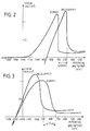
- FIG. 1 shows a basic electrochemical structure of an etching apparatus.
- This consists of an etching vessel 12 in which there is a reference electrode 15 - for example made of Hg / HgO -, a counter electrode 16 - for example made of Pt -, a silicon sample 13 as working electrode and the electrolyte 18 - for example KOH.
- the electrodes 13, 15, 16 mentioned are controlled via a potentiostat 17.
- An optical structure serves as the light source 11, which ensures largely uniform, parallel irradiation of the silicon substrate.
- the selectivity of the illumination is generated by a shadow mask 14, which is located directly on the silicon wafer, for example in the form of a metallic thin film coating.
- a focusable laser beam can also be used as the radiation source, which computer-controlled scans the pane with the desired pattern (FIGS. 4 to 7).
- the requirement for the radiation source is that, according to the band gap of the silicon, it has a light wavelength of less than 1.1 ⁇ m. So normal visible light can be used.
- This light-controlled, selective etching has created a diversity, particularly in the field of micromechanics as well as in microelectronics, for the production of microstructures and components, for which the following exemplary embodiments are intended to testify.
- Structures with vertical (100) planes as side boundaries or walls can be produced on silicon wafers with crystal orientation (100) using high-proof KOH solutions.
- the lateral undercut effect is the same size as the vertical one, so that high aspect ratios cannot be achieved in a reproducible manner.
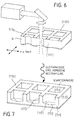
- the vertical etching rate can be significantly increased compared to the lateral one. Cuboid column structures - as illustrated for example in FIG. 4 - can now be produced with well-defined, vertical side walls.
- FIG. 5 shows an analogous application.
- cooling channels for laser mirrors, solar cells or similarly fine-structured components are shown, which are produced according to the proposed method.
- trench trenches with a width of approx. 1 ⁇ m for the arrangement of isolation trenches for high-performance components. So far, these have been produced using customary known dry etching methods, it being very difficult to achieve trenches with high aspect ratios and good slope steepness.
- FIG. 8a When generating micromechanical mesa structures, the problem of undercutting at convex corners generally arises, as illustrated in FIG. 8a. This is the case, for example, when structuring the seismic mass of a micromechanical acceleration sensor.
- an opaque shadow mask - for example a metallic thin film - and the lighting with simultaneous dark passivation potential bring a very significant improvement (Fig. 8b).
- the thickness of a membrane can be controlled by the depth of penetration of light into the material, as illustrated in FIG. 9.
- the previously complex and expensive epitaxy for membrane production is now a thing of the past.
Landscapes
- Weting (AREA)
Applications Claiming Priority (2)
| Application Number | Priority Date | Filing Date | Title |
|---|---|---|---|
| DE4036895A DE4036895A1 (de) | 1990-11-20 | 1990-11-20 | Elektrochemisches verfahren zum anisotropen aetzen von silizium |
| DE4036895 | 1990-11-20 |
Publications (2)
| Publication Number | Publication Date |
|---|---|
| EP0486873A1 true EP0486873A1 (fr) | 1992-05-27 |
| EP0486873B1 EP0486873B1 (fr) | 1997-05-14 |
Family
ID=6418584
Family Applications (1)
| Application Number | Title | Priority Date | Filing Date |
|---|---|---|---|
| EP91118871A Expired - Lifetime EP0486873B1 (fr) | 1990-11-20 | 1991-11-06 | Méthode électrochimique pour gravure anisotropique de silicium |
Country Status (3)
| Country | Link |
|---|---|
| EP (1) | EP0486873B1 (fr) |
| JP (1) | JP3187885B2 (fr) |
| DE (1) | DE4036895A1 (fr) |
Cited By (1)
| Publication number | Priority date | Publication date | Assignee | Title |
|---|---|---|---|---|
| US5338415A (en) * | 1992-06-22 | 1994-08-16 | The Regents Of The University Of California | Method for detection of chemicals by reversible quenching of silicon photoluminescence |
Families Citing this family (8)
| Publication number | Priority date | Publication date | Assignee | Title |
|---|---|---|---|---|
| EP0630058A3 (fr) * | 1993-05-19 | 1995-03-15 | Siemens Ag | Procédé de fabrication d'un arrangement de pyrodétecteurs par gravure électrochimique d'un substrat de silicium. |
| DE4328628A1 (de) * | 1993-08-20 | 1994-01-20 | Ulrich Prof Dr Mohr | Verfahren zur Herstellung einer geometrischen strukturierten Oxidschicht auf einem Siliziumkörper |
| DE19710375C2 (de) * | 1997-03-13 | 2002-11-07 | Micronas Semiconductor Holding | Verfahren zum Herstellen von räumlich strukturierten Bauteilen |
| DE102004037128A1 (de) * | 2004-07-30 | 2006-03-23 | Robert Bosch Gmbh | Laserbearbeitung von mikromechanischen Strukturen |
| US7494936B2 (en) * | 2005-05-16 | 2009-02-24 | Technion Research & Development Foundation Ltd. | Method for electrochemical etching of semiconductor material using positive potential dissolution (PPD) in solutions free from hydrogen fluoride (HF) |
| US20070256937A1 (en) * | 2006-05-04 | 2007-11-08 | International Business Machines Corporation | Apparatus and method for electrochemical processing of thin films on resistive substrates |
| CN113930846A (zh) * | 2021-12-15 | 2022-01-14 | 南京日托光伏新能源有限公司 | 匹配氢氧化钠单晶制绒方法 |
| EP4653077A1 (fr) * | 2024-05-24 | 2025-11-26 | Stichting IMEC Nederland | Procédé de fabrication d'une membrane à trous traversants |
Citations (4)
| Publication number | Priority date | Publication date | Assignee | Title |
|---|---|---|---|---|
| FR2070873A1 (fr) * | 1969-12-16 | 1971-09-17 | Western Electric Co | |
| EP0037876A2 (fr) * | 1980-03-27 | 1981-10-21 | International Business Machines Corporation | Procédé pour l'attaque électrochimique de semiconducteurs |
| US4369099A (en) * | 1981-01-08 | 1983-01-18 | Bell Telephone Laboratories, Incorporated | Photoelectrochemical etching of semiconductors |
| US4482443A (en) * | 1983-12-30 | 1984-11-13 | At&T Technologies | Photoelectrochemical etching of n-type silicon |
Family Cites Families (1)
| Publication number | Priority date | Publication date | Assignee | Title |
|---|---|---|---|---|
| US4414066A (en) * | 1982-09-10 | 1983-11-08 | Bell Telephone Laboratories, Incorporated | Electrochemical photoetching of compound semiconductors |
-
1990
- 1990-11-20 DE DE4036895A patent/DE4036895A1/de active Granted
-
1991
- 1991-11-06 EP EP91118871A patent/EP0486873B1/fr not_active Expired - Lifetime
- 1991-11-14 JP JP29910191A patent/JP3187885B2/ja not_active Expired - Fee Related
Patent Citations (4)
| Publication number | Priority date | Publication date | Assignee | Title |
|---|---|---|---|---|
| FR2070873A1 (fr) * | 1969-12-16 | 1971-09-17 | Western Electric Co | |
| EP0037876A2 (fr) * | 1980-03-27 | 1981-10-21 | International Business Machines Corporation | Procédé pour l'attaque électrochimique de semiconducteurs |
| US4369099A (en) * | 1981-01-08 | 1983-01-18 | Bell Telephone Laboratories, Incorporated | Photoelectrochemical etching of semiconductors |
| US4482443A (en) * | 1983-12-30 | 1984-11-13 | At&T Technologies | Photoelectrochemical etching of n-type silicon |
Non-Patent Citations (4)
| Title |
|---|
| IEEE TRANSACTIONS ON ELECTRON DEVICES Bd. 36, Nr. 4, April 1989, NEW YORK US Seiten 663 - 669; BEN KLOECK ET AL.: 'Study of electrochemical etch-stop for high-precision thickness control of Silicon membranes' * |
| JOURNAL OF THE ELECTROCHEMICAL SOCIETY. Bd. 131, Nr. 1, Januar 1984, MANCHESTER, NEW HAMPSHIRE US Seiten 27 - 34; EDOUARD HAROUTIOUNIAN ET AL.: 'Electrochemical and photoelectrochemical behavior and selective etching of III-V semiconductors in H2O2 as redox system' * |
| JOURNAL OF VACUUM SCIENCE AND TECHNOLOGY: PART B. Bd. 1, Nr. 1, Januar 1983, NEW YORK US Seiten 48 - 53; S. MENEZES ET AL.: 'Electrodissolution and passivation phenomena in III-V semiconducting compounds' * |
| PATENT ABSTRACTS OF JAPAN vol. 9, no. 31 (E-295)9. Februar 1985 & JP-A-59 175 127 ( DAINIPPON INSATSU K.K. ) 3. Oktober 1984 * |
Cited By (1)
| Publication number | Priority date | Publication date | Assignee | Title |
|---|---|---|---|---|
| US5338415A (en) * | 1992-06-22 | 1994-08-16 | The Regents Of The University Of California | Method for detection of chemicals by reversible quenching of silicon photoluminescence |
Also Published As
| Publication number | Publication date |
|---|---|
| DE4036895C2 (fr) | 1993-03-11 |
| DE4036895A1 (de) | 1992-05-21 |
| JPH04267524A (ja) | 1992-09-24 |
| JP3187885B2 (ja) | 2001-07-16 |
| EP0486873B1 (fr) | 1997-05-14 |
Similar Documents
| Publication | Publication Date | Title |
|---|---|---|
| DE69305955T2 (de) | Beschleunigungssensor und seine herstellung | |
| DE69433361T2 (de) | Herstellungsmethode von selbstmontierenden Mikrostrukturen | |
| DE4341271B4 (de) | Beschleunigungssensor aus kristallinem Material und Verfahren zur Herstellung dieses Beschleunigungssensors | |
| DE69839042T2 (de) | Vergrabene schicht mit hoher leitfähigkeit in einem optischen wellenleiter | |
| DE602004012590T2 (de) | Verfahren und systeme zum versehen von mems-vorrichtungen mit einer oberkappe und oberen erfassungsplatte | |
| DE4331798B4 (de) | Verfahren zur Herstellung von mikromechanischen Bauelementen | |
| DE19921241A1 (de) | Verfahren zur Herstellung eines Halbleitersensors für eine dynamische Größe | |
| WO2002036484A1 (fr) | Composant micromecanique et procede de production correspondant | |
| DE4016472C2 (fr) | ||
| EP0539393A1 (fr) | Detecteur de vitesse de rotation micromecanique. | |
| EP0486873B1 (fr) | Méthode électrochimique pour gravure anisotropique de silicium | |
| DE4030466C2 (de) | Piezo-Widerstandsvorrichtung | |
| EP1345842A2 (fr) | Procede de production d'un composant semi-conducteur et composant semi-conducteur produit selon ce procede et ayant notamment une masse mobile | |
| DE4000496A1 (de) | Verfahren zur strukturierung eines halbleiterkoerpers | |
| EP1373129A2 (fr) | Procede de production de detecteurs micromecaniques, et detecteurs ainsi obtenus | |
| DE4318466A1 (de) | Mikromechanischer Sensor und Verfahren zu dessen Herstellung | |
| DE4106287A1 (de) | Verfahren zum anisotropen aetzen von monokristallinen, scheibenfoermigen traegern | |
| DE4106933B4 (de) | Strukturierungsverfahren | |
| DE19527314A1 (de) | Siliziummembran und Verfahren zur Herstellung einer Siliziummembran | |
| DE102008026886B4 (de) | Verfahren zur Strukturierung einer Nutzschicht eines Substrats | |
| US4999083A (en) | Method of etching crystalline material with etchant injection inlet | |
| DE102016200499B4 (de) | Mikromechanisches Bauelement mit Diffusionsstoppkanal | |
| WO2004016547A1 (fr) | Procede pour fabriquer un dispositif micromecanique, notamment un miroir oscillant micromecanique | |
| DE19603829A1 (de) | Verfahren zur Herstellung von mikromechanischen Strukturen aus Silizium | |
| DE3900526C2 (fr) |
Legal Events
| Date | Code | Title | Description |
|---|---|---|---|
| PUAI | Public reference made under article 153(3) epc to a published international application that has entered the european phase |
Free format text: ORIGINAL CODE: 0009012 |
|
| AK | Designated contracting states |
Kind code of ref document: A1 Designated state(s): FR GB IT |
|
| 17P | Request for examination filed |
Effective date: 19920617 |
|
| 17Q | First examination report despatched |
Effective date: 19921026 |
|
| RAP1 | Party data changed (applicant data changed or rights of an application transferred) |
Owner name: DEUTSCHE AEROSPACE AKTIENGESELLSCHAFT |
|
| RAP1 | Party data changed (applicant data changed or rights of an application transferred) |
Owner name: DAIMLER-BENZ AEROSPACE AKTIENGESELLSCHAFT |
|
| GRAG | Despatch of communication of intention to grant |
Free format text: ORIGINAL CODE: EPIDOS AGRA |
|
| GRAH | Despatch of communication of intention to grant a patent |
Free format text: ORIGINAL CODE: EPIDOS IGRA |
|
| GRAH | Despatch of communication of intention to grant a patent |
Free format text: ORIGINAL CODE: EPIDOS IGRA |
|
| RAP1 | Party data changed (applicant data changed or rights of an application transferred) |
Owner name: DAIMLER-BENZ AKTIENGESELLSCHAFT |
|
| GRAA | (expected) grant |
Free format text: ORIGINAL CODE: 0009210 |
|
| AK | Designated contracting states |
Kind code of ref document: B1 Designated state(s): FR GB IT |
|
| GBT | Gb: translation of ep patent filed (gb section 77(6)(a)/1977) |
Effective date: 19970515 |
|
| ET | Fr: translation filed | ||
| PLBE | No opposition filed within time limit |
Free format text: ORIGINAL CODE: 0009261 |
|
| STAA | Information on the status of an ep patent application or granted ep patent |
Free format text: STATUS: NO OPPOSITION FILED WITHIN TIME LIMIT |
|
| 26N | No opposition filed | ||
| REG | Reference to a national code |
Ref country code: GB Ref legal event code: 732E |
|
| REG | Reference to a national code |
Ref country code: FR Ref legal event code: TP |
|
| PGFP | Annual fee paid to national office [announced via postgrant information from national office to epo] |
Ref country code: GB Payment date: 20011012 Year of fee payment: 11 |
|
| PGFP | Annual fee paid to national office [announced via postgrant information from national office to epo] |
Ref country code: FR Payment date: 20011106 Year of fee payment: 11 |
|
| REG | Reference to a national code |
Ref country code: GB Ref legal event code: IF02 |
|
| PG25 | Lapsed in a contracting state [announced via postgrant information from national office to epo] |
Ref country code: GB Free format text: LAPSE BECAUSE OF NON-PAYMENT OF DUE FEES Effective date: 20021106 |
|
| GBPC | Gb: european patent ceased through non-payment of renewal fee | ||
| PG25 | Lapsed in a contracting state [announced via postgrant information from national office to epo] |
Ref country code: FR Free format text: LAPSE BECAUSE OF NON-PAYMENT OF DUE FEES Effective date: 20030731 |
|
| REG | Reference to a national code |
Ref country code: FR Ref legal event code: ST |
|
| PG25 | Lapsed in a contracting state [announced via postgrant information from national office to epo] |
Ref country code: IT Free format text: LAPSE BECAUSE OF NON-PAYMENT OF DUE FEES;WARNING: LAPSES OF ITALIAN PATENTS WITH EFFECTIVE DATE BEFORE 2007 MAY HAVE OCCURRED AT ANY TIME BEFORE 2007. THE CORRECT EFFECTIVE DATE MAY BE DIFFERENT FROM THE ONE RECORDED. Effective date: 20051106 |