EP0486985B1 - Komparator - Google Patents
Komparator Download PDFInfo
- Publication number
- EP0486985B1 EP0486985B1 EP91119630A EP91119630A EP0486985B1 EP 0486985 B1 EP0486985 B1 EP 0486985B1 EP 91119630 A EP91119630 A EP 91119630A EP 91119630 A EP91119630 A EP 91119630A EP 0486985 B1 EP0486985 B1 EP 0486985B1
- Authority
- EP
- European Patent Office
- Prior art keywords
- transistor
- transistors
- current mirror
- constant current
- comparator
- Prior art date
- Legal status (The legal status is an assumption and is not a legal conclusion. Google has not performed a legal analysis and makes no representation as to the accuracy of the status listed.)
- Expired - Lifetime
Links
- 238000010586 diagram Methods 0.000 description 5
- 230000008878 coupling Effects 0.000 description 3
- 238000010168 coupling process Methods 0.000 description 3
- 238000005859 coupling reaction Methods 0.000 description 3
- 238000009738 saturating Methods 0.000 description 2
- 238000010276 construction Methods 0.000 description 1
- 230000007257 malfunction Effects 0.000 description 1
Images
Classifications
-
- G—PHYSICS
- G01—MEASURING; TESTING
- G01R—MEASURING ELECTRIC VARIABLES; MEASURING MAGNETIC VARIABLES
- G01R19/00—Arrangements for measuring currents or voltages or for indicating presence or sign thereof
- G01R19/0038—Circuits for comparing several input signals and for indicating the result of this comparison, e.g. equal, different, greater, smaller (comparing pulses or pulse trains according to amplitude)
Definitions
- the invention relates to a comparator.
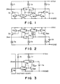
- Fig. 3 shows an example of a circuit of a conventional comparator.
- V 3 denotes a reference voltage source;
- I 7 indicates a constant current source;
- a circuit which is constructed by the constant current source I 7 and the transistors Q 21 to Q 24 is a simple comparator.
- An input terminal IN and the resistor R 2 are connected to a base of the transistor Q 21 and a base of the transistor Q 25 through wires and connectors from another electronic circuit board, respectively.
- the transistor Q 25 is turned off and the circuit operates as an ordinary comparator.
- an output of the comparator is an output in a state in which a high level signal has been applied to an input.
- the transistor Q 25 connected by the resistor R 1 is set into a saturation state by a power source V cc , thereby fixing a base potential of the transistor Q 21 to a low level and satisfying the logic.
- the conventional comparator has the following technical problems to be solved.
- a comparator for turning on/off an input terminal comprising a first constant current source; a differential amplifier connected to said first constant current source; a first current mirror circuit connected to said differential amplifier; second and third current mirror circuits connected to both sides of said differential amplifier and said first current mirror circuit, respectively; said first, second and third current mirror circuits comprising transistors; and second and third constant current sources connected to both sides of said second and third current mirror circuits, respectively; said second current mirror circuit and said second constant current source constituting a control circuit to enable the transistor of said second current mirror circuit connected to said differential amplifier in a high impedance input state.
- the high impedance input state can be detected by the above construction without additionally providing any wire and connector.
- Fig. 1 is a circuit constructional diagram showing most preferably a feature of the invention.
- V 1 denotes a reference voltage source
- I 1 to I 3 indicate constant current sources
- Q 1 to Q 10 indicate transistors.
- a circuit which is constructed by the constant current source I 2 and the transistors Q 4 to Q 7 is a comparator.
- Current mirror circuits are constructed by the transistors Q 2 and Q 3 and the transistors Q 8 and Q 9 .
- the constant current source I 1 and the transistor Q 1 supply a constant current to the current mirror circuit.
- the constant current source I 3 and the transistor Q 10 supply a constant current to the current mirror circuit.
- a collector of the transistor Q 3 pulls in a current which is equivalent to a base current of the transistor Q 1 from the base of the transistor Q 4 and the terminal IN.
- the circuit operates as an ordinary comparator.
- Fig. 2 is a circuit constructional diagram showing another embodiment of the invention.
- V 2 denotes a reference voltage source; I 4 to I 6 constant current sources; and Q 11 to Q 20 transistors.
- a circuit which is constructed by the constant current source I 5 and the transistors Q 14 to Q 17 is a comparator.
- Current mirror circuits are constructed by the transistors Q 12 and Q 13 and the transistors Q 18 and Q 19 .
- the constant current source I 4 and the transistor Q 11 function as a constant current source which is supplied to the current mirror circuit.
- the constant current source I 6 and the transistor Q 20 function as a constant current source which is supplied to the current mirror circuit.
- a collector of the transistor Q 13 supplies a current which is equivalent to a base current of the transistor Q 11 to the base of the transistor Q 14 and the terminal IN.
- the circuit operates as an ordinary comparator.
- the input disconnection state can be certainly known without increasing the costs.
Landscapes
- Physics & Mathematics (AREA)
- General Physics & Mathematics (AREA)
- Manipulation Of Pulses (AREA)
- Measurement Of Current Or Voltage (AREA)
- Electronic Switches (AREA)
- Amplifiers (AREA)
Claims (3)
- Komparator zum Ein-/Ausschalten eines Eingangsanschlusses (IN) miteiner ersten Konstantstromquelle (I2; I5),einem an die erste Konstantstromquelle (I2; I5) angeschlossenen Differenzverstärker (Q4, Q5; Q14, Q15),einer an den Differenzverstärker (Q4, Q5; Q14, Q15) angeschlossenen ersten Stromspiegelschaltung (Q6, Q7; Q16, Q11),jeweils an beide Seiten des Differenzverstärkers (Q4, Q5; Q14, Q15) und der ersten Stromspiegelschaltung (Q6, Q7; Q16, Q17) angeschlossenen zweiten und dritten Stromspiegelschaltungen (Q2, Q3, Q8, Q9; Q12, Q13, Q18, Q19),wobei die ersten, zweiten und dritten Stromspiegelschaltungen (Q6, Q7, Q2, Q3, Q8, Q9; Q16, Q17, Q12, Q13, Q18, Q19) Transistoren umfassen sowiejeweils an beide Seiten der zweiten und dritten Stromspiegelschaltungen (Q2, Q3, Q8, Q9; Q12, Q13, Q18, Q19) angeschlossenen zweiten und dritten Konstantstromquellen (I1, Q2, I3, Q10; I4, Q11, I6, Q20),wobei die zweite Stromspiegelschaltung (Q1, Q3; Q12, Q13) und die zweite Konstantstromquelle (I1, Q1; I4, Q11) eine Steuerschaltung (Q1, Q2, Q3, I1; Q11, Q12, Q13, I4) bilden, damit der Transistor der an den Differenzverstärker (Q4, Q5; Q14, Q15) angeschlossenen zweiten Stromspiegelschaltung (Q2, Q3; Q12, Q13) in einem hochohmigen Eingangszustand eingeschaltet werden kann.
- Komparator nach Anspruch 1, wobeider Differenzverstärker (Q4, Q5; Q14, Q15) ein Paar von Transistoren (Q4, Q5; Q14, Q15) aufweist, die an den Eingangsanschluß (IN), dem ein Eingangssignal zugeführt wird, und zur Zufuhr eines Ausgangssignals an einen Ausgangsanschluß (OUT) angeschlossen sind, wobei die Basis eines (Q4; Q14) des Paars von Transistoren (Q4, Q5; Q14, Q15) an den Eingangsanschluß (IN) und der Kollektor des anderen (Q5; Q15) des Paars von Transistoren (Q4, Q5; Q14, Q15) an den Ausgangsanschluß (OUT) angeschlossen ist unddie Steuerschaltung (Q1, Q2, Q3, I1; Q11, Q12, Q13, I4) zur Steuerung eines auf den hochohmigen Zustand des Eingangsanschlusses (IN) ansprechenden Potentials des Eingangsanschlusses (IN) mit dem Eingangsanschluß (IN) verbunden ist,wobei die dritte Stromspiegelschaltung (Q8, Q9; Q18, Q19) und die dritte Konstantstromspannungsquelle (I3, Q10; I6, Q20) eine mit der Steuerschaltung (Q1, Q2, Q3, I1; Q11, Q12, Q13, I4) identische und an den anderen (Q5; Q15) des an den Ausgangsanschluß (OUT) angeschlossen Paars von Transistoren (Q4, Q5; Q14, Q15) angeschlossene weitere Steuerschaltung (Q8, Q9, Q10, I3; Q18, Q19, Q20, I6) bilden.
- Komparator nach Anspruch 1 oder 2, wobei jede der zweiten und dritten Konstantstromquellen (I1, Q1, I3, Q10; I4, Q11, I6, Q20) jeweils eine Stromquelle ((I1, I3, I4, I6) und einen weiteren Transistor (Q1, Q10; Q11, Q20) zur Zufuhr eines Stroms zu den zweiten und dritten Stromspiegelschaltungen (Q2, Q3, Q8, Q9; Q12, Q13, Q18, 19) umfaßt.
Applications Claiming Priority (2)
| Application Number | Priority Date | Filing Date | Title |
|---|---|---|---|
| JP311278/90 | 1990-11-19 | ||
| JP2311278A JP2921968B2 (ja) | 1990-11-19 | 1990-11-19 | 比較器 |
Publications (3)
| Publication Number | Publication Date |
|---|---|
| EP0486985A2 EP0486985A2 (de) | 1992-05-27 |
| EP0486985A3 EP0486985A3 (en) | 1992-09-09 |
| EP0486985B1 true EP0486985B1 (de) | 1997-03-05 |
Family
ID=18015210
Family Applications (1)
| Application Number | Title | Priority Date | Filing Date |
|---|---|---|---|
| EP91119630A Expired - Lifetime EP0486985B1 (de) | 1990-11-19 | 1991-11-18 | Komparator |
Country Status (4)
| Country | Link |
|---|---|
| US (1) | US5313115A (de) |
| EP (1) | EP0486985B1 (de) |
| JP (1) | JP2921968B2 (de) |
| DE (1) | DE69124926T2 (de) |
Families Citing this family (1)
| Publication number | Priority date | Publication date | Assignee | Title |
|---|---|---|---|---|
| JP7523904B2 (ja) | 2019-12-27 | 2024-07-29 | キヤノン株式会社 | 検査装置および半導体装置の製造方法 |
Family Cites Families (8)
| Publication number | Priority date | Publication date | Assignee | Title |
|---|---|---|---|---|
| US3942044A (en) * | 1974-03-08 | 1976-03-02 | U.S. Philips Corporation | Interface receiver |
| JPS50156348A (de) * | 1974-06-04 | 1975-12-17 | ||
| UST957008I4 (en) * | 1976-04-12 | 1977-04-05 | Rca Corporation | Switching circuit with accurate current threshold |
| DE2944657C2 (de) * | 1979-11-06 | 1985-02-14 | Robert Bosch Gmbh, 7000 Stuttgart | Komparatorschaltung |
| DE3582620D1 (de) * | 1984-07-27 | 1991-05-29 | Omron Tateisi Electronics Co | Einschalt-ruecksetzschaltung fuer einen beruehrungslosen schalter. |
| JPH0720205B2 (ja) * | 1985-02-28 | 1995-03-06 | キヤノン株式会社 | 同期分離回路 |
| JP2779411B2 (ja) * | 1985-03-01 | 1998-07-23 | キヤノン株式会社 | スイツチング装置 |
| US4871926A (en) * | 1988-09-06 | 1989-10-03 | Motorola, Inc. | Low power, three state power up circuit |
-
1990
- 1990-11-19 JP JP2311278A patent/JP2921968B2/ja not_active Expired - Lifetime
-
1991
- 1991-11-18 US US07/793,521 patent/US5313115A/en not_active Expired - Lifetime
- 1991-11-18 DE DE69124926T patent/DE69124926T2/de not_active Expired - Lifetime
- 1991-11-18 EP EP91119630A patent/EP0486985B1/de not_active Expired - Lifetime
Non-Patent Citations (1)
| Title |
|---|
| U. Tietze, Ch. Schenk "Halbleiter-Schaltungstechnik", 10th. edition, Springer-Verlag, pages 66-67 * |
Also Published As
| Publication number | Publication date |
|---|---|
| EP0486985A2 (de) | 1992-05-27 |
| US5313115A (en) | 1994-05-17 |
| JPH04183018A (ja) | 1992-06-30 |
| DE69124926D1 (de) | 1997-04-10 |
| DE69124926T2 (de) | 1997-07-03 |
| JP2921968B2 (ja) | 1999-07-19 |
| EP0486985A3 (en) | 1992-09-09 |
Similar Documents
| Publication | Publication Date | Title |
|---|---|---|
| US4748426A (en) | Active termination circuit for computer interface use | |
| US4453092A (en) | Comparator circuit having reduced input bias current | |
| EP0238803B1 (de) | Stabilisierte Konstantstromversorgung | |
| KR970003720B1 (ko) | 전기신호 증폭기 장치 | |
| EP0486985B1 (de) | Komparator | |
| EP0391055A2 (de) | Ausgangsstufe für einen Operationsverstärker | |
| US4525637A (en) | Integrated circuit having an input voltage-clamping function and an input current-detecting function | |
| JPS6364084B2 (de) | ||
| US4801825A (en) | Three level state logic circuit having improved high voltage to high output impedance transition | |
| US5027016A (en) | Low power transient suppressor circuit | |
| JP3466717B2 (ja) | ラインドライバ‐スイッチング段 | |
| US5317470A (en) | Control system including a switching circuit for ensuring proper operation when operating power is removed from a portion of the control system | |
| EP0868688B1 (de) | Rücksetzstellungsschaltung zur sicherstellung der korrekten rücksetzstellung für den fall zusammenbrechender stromversorgung | |
| US4970416A (en) | Emitter coupled logic circuit having rapid output voltage | |
| US6553499B1 (en) | Low power circuit for waking from a sleep mode by using a remote power-on signal | |
| US5936389A (en) | Terminating resistance circuit | |
| US7107465B1 (en) | PCI bus interface circuit for supplying either a main supply voltage or an auxiliary voltage to a PCI plug-in-card | |
| US5764105A (en) | Push-pull output circuit method | |
| JP2615890B2 (ja) | 制御機器の入力装置 | |
| US5825160A (en) | Power control circuit in wireless mobile communication system | |
| US5397935A (en) | Bias current supplying circuit | |
| JPS6319097A (ja) | 線路異常監視装置 | |
| US6204702B1 (en) | Arrangement for supplying circuits with direct currents | |
| US4345216A (en) | Compensation of base-current-related error in current mirror amplifier circuitry | |
| US5434517A (en) | ECL output buffer with a MOS transistor used for tristate enable |
Legal Events
| Date | Code | Title | Description |
|---|---|---|---|
| PUAI | Public reference made under article 153(3) epc to a published international application that has entered the european phase |
Free format text: ORIGINAL CODE: 0009012 |
|
| AK | Designated contracting states |
Kind code of ref document: A2 Designated state(s): DE FR GB IT NL |
|
| PUAL | Search report despatched |
Free format text: ORIGINAL CODE: 0009013 |
|
| AK | Designated contracting states |
Kind code of ref document: A3 Designated state(s): DE FR GB IT NL |
|
| 17P | Request for examination filed |
Effective date: 19930122 |
|
| 17Q | First examination report despatched |
Effective date: 19950119 |
|
| GRAG | Despatch of communication of intention to grant |
Free format text: ORIGINAL CODE: EPIDOS AGRA |
|
| GRAH | Despatch of communication of intention to grant a patent |
Free format text: ORIGINAL CODE: EPIDOS IGRA |
|
| GRAH | Despatch of communication of intention to grant a patent |
Free format text: ORIGINAL CODE: EPIDOS IGRA |
|
| GRAA | (expected) grant |
Free format text: ORIGINAL CODE: 0009210 |
|
| AK | Designated contracting states |
Kind code of ref document: B1 Designated state(s): DE FR GB IT NL |
|
| REF | Corresponds to: |
Ref document number: 69124926 Country of ref document: DE Date of ref document: 19970410 |
|
| ET | Fr: translation filed | ||
| ITF | It: translation for a ep patent filed | ||
| PLBE | No opposition filed within time limit |
Free format text: ORIGINAL CODE: 0009261 |
|
| STAA | Information on the status of an ep patent application or granted ep patent |
Free format text: STATUS: NO OPPOSITION FILED WITHIN TIME LIMIT |
|
| 26N | No opposition filed | ||
| REG | Reference to a national code |
Ref country code: GB Ref legal event code: IF02 |
|
| PGFP | Annual fee paid to national office [announced via postgrant information from national office to epo] |
Ref country code: NL Payment date: 20081118 Year of fee payment: 18 |
|
| PGFP | Annual fee paid to national office [announced via postgrant information from national office to epo] |
Ref country code: IT Payment date: 20081119 Year of fee payment: 18 |
|
| PGFP | Annual fee paid to national office [announced via postgrant information from national office to epo] |
Ref country code: FR Payment date: 20081124 Year of fee payment: 18 |
|
| PGFP | Annual fee paid to national office [announced via postgrant information from national office to epo] |
Ref country code: GB Payment date: 20091204 Year of fee payment: 19 |
|
| REG | Reference to a national code |
Ref country code: NL Ref legal event code: V1 Effective date: 20100601 |
|
| PGFP | Annual fee paid to national office [announced via postgrant information from national office to epo] |
Ref country code: DE Payment date: 20091130 Year of fee payment: 19 |
|
| REG | Reference to a national code |
Ref country code: FR Ref legal event code: ST Effective date: 20100730 |
|
| PG25 | Lapsed in a contracting state [announced via postgrant information from national office to epo] |
Ref country code: FR Free format text: LAPSE BECAUSE OF NON-PAYMENT OF DUE FEES Effective date: 20091130 Ref country code: NL Free format text: LAPSE BECAUSE OF NON-PAYMENT OF DUE FEES Effective date: 20100601 |
|
| PG25 | Lapsed in a contracting state [announced via postgrant information from national office to epo] |
Ref country code: IT Free format text: LAPSE BECAUSE OF NON-PAYMENT OF DUE FEES Effective date: 20091118 |
|
| GBPC | Gb: european patent ceased through non-payment of renewal fee |
Effective date: 20101118 |
|
| REG | Reference to a national code |
Ref country code: DE Ref legal event code: R119 Ref document number: 69124926 Country of ref document: DE Effective date: 20110601 Ref country code: DE Ref legal event code: R119 Ref document number: 69124926 Country of ref document: DE Effective date: 20110531 |
|
| PG25 | Lapsed in a contracting state [announced via postgrant information from national office to epo] |
Ref country code: DE Free format text: LAPSE BECAUSE OF NON-PAYMENT OF DUE FEES Effective date: 20110531 |
|
| PG25 | Lapsed in a contracting state [announced via postgrant information from national office to epo] |
Ref country code: GB Free format text: LAPSE BECAUSE OF NON-PAYMENT OF DUE FEES Effective date: 20101118 |