EP0486986A1 - Pufferschaltung - Google Patents
Pufferschaltung Download PDFInfo
- Publication number
- EP0486986A1 EP0486986A1 EP91119631A EP91119631A EP0486986A1 EP 0486986 A1 EP0486986 A1 EP 0486986A1 EP 91119631 A EP91119631 A EP 91119631A EP 91119631 A EP91119631 A EP 91119631A EP 0486986 A1 EP0486986 A1 EP 0486986A1
- Authority
- EP
- European Patent Office
- Prior art keywords
- input
- transistor
- buffer circuit
- transistors
- voltage
- Prior art date
- Legal status (The legal status is an assumption and is not a legal conclusion. Google has not performed a legal analysis and makes no representation as to the accuracy of the status listed.)
- Granted
Links
- 239000004065 semiconductor Substances 0.000 claims description 3
- 238000010586 diagram Methods 0.000 description 3
- 230000003503 early effect Effects 0.000 description 2
- 230000015572 biosynthetic process Effects 0.000 description 1
- 238000006243 chemical reaction Methods 0.000 description 1
- 230000007257 malfunction Effects 0.000 description 1
- 239000000758 substrate Substances 0.000 description 1
Images

Classifications
-
- H—ELECTRICITY
- H03—ELECTRONIC CIRCUITRY
- H03F—AMPLIFIERS
- H03F3/00—Amplifiers with only discharge tubes or only semiconductor devices as amplifying elements
- H03F3/30—Single-ended push-pull [SEPP] amplifiers; Phase-splitters therefor
- H03F3/3069—Single-ended push-pull [SEPP] amplifiers; Phase-splitters therefor the emitters of complementary power transistors being connected to the output
- H03F3/3076—Single-ended push-pull [SEPP] amplifiers; Phase-splitters therefor the emitters of complementary power transistors being connected to the output with symmetrical driving of the end stage
-
- H—ELECTRICITY
- H03—ELECTRONIC CIRCUITRY
- H03F—AMPLIFIERS
- H03F1/00—Details of amplifiers with only discharge tubes, only semiconductor devices or only unspecified devices as amplifying elements
- H03F1/30—Modifications of amplifiers to reduce influence of variations of temperature or supply voltage or other physical parameters
- H03F1/307—Modifications of amplifiers to reduce influence of variations of temperature or supply voltage or other physical parameters in push-pull amplifiers
-
- H—ELECTRICITY
- H03—ELECTRONIC CIRCUITRY
- H03F—AMPLIFIERS
- H03F3/00—Amplifiers with only discharge tubes or only semiconductor devices as amplifying elements
- H03F3/34—DC amplifiers in which all stages are DC-coupled
- H03F3/343—DC amplifiers in which all stages are DC-coupled with semiconductor devices only
Definitions
- This invention relates to a buffer circuit for use in, for example, impedance conversion, an input unit for current feedback type operational amplifiers and the like.
- the buffer circuit is composed of diode-connected transistors 15 and 16 which are opposite to each other in polarity, transistors 17 and 18 matching those transistors 15 and 16 respectively, and constant-current sources 19 and 20 for feeding constant current to the transistors 15 and 16 as shown in Fig. 1.
- the transistors 15 and 17, and the transistors 16 and 18, for which matching is required respectively are operated by a different C-E (Collector-Emitter) voltage. Therefore, an offset appears between input (IN) and output (OUT) due to the Early's effect of transistors, possibly causing a malfunction.
- C-E collector-emitter
- the offset between the input and output terminals can be reduced for correct operations by the provision of a transistor which keeps constant the difference in the collector-emitter (C-E) voltage between transistors for which matching is required.
- FIG. 2 A preferred embodiment of the present invention is best shown in Fig. 2.
- numeral 1 is an input terminal
- numeral 2 is an output terminal.
- Transistors 3 and 4 which are opposite to each other in polarity, are connected with the input terminal 1, and are biased by constant-current sources 11 and 12 respectively.
- Transistors 5 and 6 are connected with the output terminal 2, and are diode-connected with a short between the base and the collector, requiring matching with those transistors 3 and 4 respectively.
- Transistors 7 and 8, and transistors 9 and 10 are used to keep constant the C-E voltage of the transistors 3 and 4, and the transistors 7 and 8 are biased by constant-current sources 13 and 14 respectively.
- the C-B voltage of the transistor 4 is kept down at 0 (V) by means of Vbe of the transistors 9 and 10, and the C-E voltage of the transistor 4 at 1 x Vbe (V). Since the transistors 3 and 5, and the transistors 4 and 6 are operating at the same C-E voltage 1 x Vbe (V), there is no difference in operating current between the two due to the Early's effect, but an offset between the input and output terminals is very small.
- the circuit described above is integrated on a semiconductor substrate for formation.
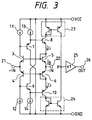
- Fig. 3 shows an example in which the above embodiment has been used as an input buffer for a current feedback type operational amplifier.
- numeral 21 is a forward input terminal
- numeral 22 is a reverse input terminal
- numerals 23 and 24 are current mirror circuits
- numeral 25 is an output buffer
- numeral 26 is an output terminal.
- An input current IN flows through the reverse input terminal 22 by an input voltage applied to between the forward and reverse input terminals, and becomes a differential current between a current I1 above and a current I2 below the reverse input terminal 22.
- This differential current flows to the output stage through current mirror circuits 23 and 24, is converted into a voltage at a point P, and is output at the output terminal 26 through an output buffer 25.
- An offset between forward 21 and reverse 22 input terminals at this time is increased by the gain times and becomes an offset at the output terminal 26.
- a buffer circuit according to the present invention is used as an input buffer, the offset between the forward 21 and reverse 22 input terminals becomes very small, and as a result, the offset at the output terminal 26 is also reduced.
- This operational amplifier consists of a semiconductor integrated circuit.
- an offset between an input and output can be reduced by keeping down at a very small value a C-E voltage difference between transistors for which matching is required to each other for operation.
- a buffer circuit provided with a transistor each on the input and output terminal sides, in which the transistor has been provided in order to keep constant a difference between a collector-emitter voltage of the input terminal side transistor and that of the output terminal side transistor.
Landscapes
- Engineering & Computer Science (AREA)
- Power Engineering (AREA)
- Amplifiers (AREA)
Applications Claiming Priority (2)
| Application Number | Priority Date | Filing Date | Title |
|---|---|---|---|
| JP02311277A JP3103104B2 (ja) | 1990-11-19 | 1990-11-19 | バッファ回路 |
| JP311277/90 | 1990-11-19 |
Publications (2)
| Publication Number | Publication Date |
|---|---|
| EP0486986A1 true EP0486986A1 (de) | 1992-05-27 |
| EP0486986B1 EP0486986B1 (de) | 1997-06-04 |
Family
ID=18015199
Family Applications (1)
| Application Number | Title | Priority Date | Filing Date |
|---|---|---|---|
| EP91119631A Expired - Lifetime EP0486986B1 (de) | 1990-11-19 | 1991-11-18 | Pufferschaltung |
Country Status (3)
| Country | Link |
|---|---|
| EP (1) | EP0486986B1 (de) |
| JP (1) | JP3103104B2 (de) |
| DE (1) | DE69126401T2 (de) |
Cited By (1)
| Publication number | Priority date | Publication date | Assignee | Title |
|---|---|---|---|---|
| US5511799A (en) * | 1993-06-07 | 1996-04-30 | Applied Materials, Inc. | Sealing device useful in semiconductor processing apparatus for bridging materials having a thermal expansion differential |
Families Citing this family (1)
| Publication number | Priority date | Publication date | Assignee | Title |
|---|---|---|---|---|
| JP5445515B2 (ja) * | 2011-05-31 | 2014-03-19 | オンキヨー株式会社 | 増幅回路 |
-
1990
- 1990-11-19 JP JP02311277A patent/JP3103104B2/ja not_active Expired - Fee Related
-
1991
- 1991-11-18 DE DE1991626401 patent/DE69126401T2/de not_active Expired - Fee Related
- 1991-11-18 EP EP91119631A patent/EP0486986B1/de not_active Expired - Lifetime
Non-Patent Citations (3)
| Title |
|---|
| ELECTRONIC DESIGN. vol. 35, no. 5, 5 March 1987, HASBROUCK HEIGHTS, NEW JERSEY pages 71 - 74; F. GOODENOUGH: 'Electronic Design Report ISSCC: ANALOG' * |
| INTERNATIONAL JOURNAL OF ELECTRONICS. vol. 57, no. 5, November 1984, LONDON GB pages 713 - 717; A. FABRE: 'An integrable multiple output translinear current convertor' * |
| INTERNATIONAL JOURNAL OF ELECTRONICS. vol. 59, no. 6, December 1985, LONDON GB pages 771 - 777; G. NORMAND: 'Translinear current conveyors' * |
Cited By (1)
| Publication number | Priority date | Publication date | Assignee | Title |
|---|---|---|---|---|
| US5511799A (en) * | 1993-06-07 | 1996-04-30 | Applied Materials, Inc. | Sealing device useful in semiconductor processing apparatus for bridging materials having a thermal expansion differential |
Also Published As
| Publication number | Publication date |
|---|---|
| JPH04183007A (ja) | 1992-06-30 |
| EP0486986B1 (de) | 1997-06-04 |
| DE69126401D1 (de) | 1997-07-10 |
| JP3103104B2 (ja) | 2000-10-23 |
| DE69126401T2 (de) | 1998-01-22 |
Similar Documents
| Publication | Publication Date | Title |
|---|---|---|
| EP0403195B1 (de) | Stromspiegelschaltung | |
| US6429700B1 (en) | Driver circuit with output common mode voltage control | |
| US5734296A (en) | Low voltage operational amplifier input stage and method | |
| US5699015A (en) | Low voltage operational amplifier and method | |
| EP0037406B1 (de) | Cmos - operationsverstärker mit verminderter verlustleistung | |
| US4152663A (en) | Amplifier arrangement | |
| EP0616421A1 (de) | Gegengekoppelter Verstärker zur Verstärkungsregelung in einer Kaskadenschaltung | |
| US5798673A (en) | Low voltage operational amplifier bias circuit and method | |
| US4855618A (en) | MOS current mirror with high output impedance and compliance | |
| EP0209987B1 (de) | Pufferverstärker mit Verstärkungsfaktor Eins | |
| EP0419819B1 (de) | Stromspiegel | |
| JPH02162812A (ja) | 相補形カレント・ミラー回路を用いたダイアモンド・フォロワ回路及びゼロ・オフセットの増幅器 | |
| EP0173370A1 (de) | Verstärkereinrichtung | |
| EP0181017B1 (de) | Transistor oder Diode simulierende Schaltungsanordnung | |
| US4779059A (en) | Current mirror circuit | |
| EP0409448A2 (de) | Operationsverstärker mit auswählbaren Eingängen | |
| EP0486986A1 (de) | Pufferschaltung | |
| EP0448169B1 (de) | Verstärkerschaltung | |
| EP0528659B1 (de) | Impedanzvervielfacher | |
| US5278516A (en) | Buffer circuit | |
| US5446414A (en) | Simple high speed precision transconductance amplifier circuits | |
| JPH09105763A (ja) | コンパレータ回路 | |
| EP0841746A2 (de) | Schnelle Pufferschaltung | |
| JPH06169225A (ja) | 電圧電流変換回路 | |
| EP0339481B1 (de) | Breitbandverstärker |
Legal Events
| Date | Code | Title | Description |
|---|---|---|---|
| PUAI | Public reference made under article 153(3) epc to a published international application that has entered the european phase |
Free format text: ORIGINAL CODE: 0009012 |
|
| AK | Designated contracting states |
Kind code of ref document: A1 Designated state(s): DE FR GB IT NL |
|
| 17P | Request for examination filed |
Effective date: 19921013 |
|
| 17Q | First examination report despatched |
Effective date: 19941027 |
|
| GRAG | Despatch of communication of intention to grant |
Free format text: ORIGINAL CODE: EPIDOS AGRA |
|
| GRAH | Despatch of communication of intention to grant a patent |
Free format text: ORIGINAL CODE: EPIDOS IGRA |
|
| GRAH | Despatch of communication of intention to grant a patent |
Free format text: ORIGINAL CODE: EPIDOS IGRA |
|
| GRAA | (expected) grant |
Free format text: ORIGINAL CODE: 0009210 |
|
| AK | Designated contracting states |
Kind code of ref document: B1 Designated state(s): DE FR GB IT NL |
|
| PG25 | Lapsed in a contracting state [announced via postgrant information from national office to epo] |
Ref country code: IT Free format text: LAPSE BECAUSE OF FAILURE TO SUBMIT A TRANSLATION OF THE DESCRIPTION OR TO PAY THE FEE WITHIN THE PRE;WARNING: LAPSES OF ITALIAN PATENTS WITH EFFECTIVE DATE BEFORE 2007 MAY HAVE OCCURRED AT ANY TIME BEFORE 2007. THE CORRECT EFFECTIVE DATE MAY BE DIFFERENT FROM THE ONE RECORDED.SCRIBED TIME-LIMIT Effective date: 19970604 Ref country code: NL Free format text: LAPSE BECAUSE OF FAILURE TO SUBMIT A TRANSLATION OF THE DESCRIPTION OR TO PAY THE FEE WITHIN THE PRESCRIBED TIME-LIMIT Effective date: 19970604 |
|
| REF | Corresponds to: |
Ref document number: 69126401 Country of ref document: DE Date of ref document: 19970710 |
|
| ET | Fr: translation filed | ||
| NLV1 | Nl: lapsed or annulled due to failure to fulfill the requirements of art. 29p and 29m of the patents act | ||
| PLBE | No opposition filed within time limit |
Free format text: ORIGINAL CODE: 0009261 |
|
| STAA | Information on the status of an ep patent application or granted ep patent |
Free format text: STATUS: NO OPPOSITION FILED WITHIN TIME LIMIT |
|
| 26N | No opposition filed | ||
| REG | Reference to a national code |
Ref country code: GB Ref legal event code: IF02 |
|
| PGFP | Annual fee paid to national office [announced via postgrant information from national office to epo] |
Ref country code: FR Payment date: 20051108 Year of fee payment: 15 |
|
| PGFP | Annual fee paid to national office [announced via postgrant information from national office to epo] |
Ref country code: DE Payment date: 20051110 Year of fee payment: 15 |
|
| PGFP | Annual fee paid to national office [announced via postgrant information from national office to epo] |
Ref country code: GB Payment date: 20051116 Year of fee payment: 15 |
|
| PG25 | Lapsed in a contracting state [announced via postgrant information from national office to epo] |
Ref country code: DE Free format text: LAPSE BECAUSE OF NON-PAYMENT OF DUE FEES Effective date: 20070601 |
|
| GBPC | Gb: european patent ceased through non-payment of renewal fee |
Effective date: 20061118 |
|
| REG | Reference to a national code |
Ref country code: FR Ref legal event code: ST Effective date: 20070731 |
|
| PG25 | Lapsed in a contracting state [announced via postgrant information from national office to epo] |
Ref country code: GB Free format text: LAPSE BECAUSE OF NON-PAYMENT OF DUE FEES Effective date: 20061118 |
|
| PG25 | Lapsed in a contracting state [announced via postgrant information from national office to epo] |
Ref country code: FR Free format text: LAPSE BECAUSE OF NON-PAYMENT OF DUE FEES Effective date: 20061130 |