EP0487548B1 - Funkrufempfänger mit synthesizer mit veränderbaren eigenschaften - Google Patents
Funkrufempfänger mit synthesizer mit veränderbaren eigenschaften Download PDFInfo
- Publication number
- EP0487548B1 EP0487548B1 EP90911065A EP90911065A EP0487548B1 EP 0487548 B1 EP0487548 B1 EP 0487548B1 EP 90911065 A EP90911065 A EP 90911065A EP 90911065 A EP90911065 A EP 90911065A EP 0487548 B1 EP0487548 B1 EP 0487548B1
- Authority
- EP
- European Patent Office
- Prior art keywords
- signal
- frequency
- selective call
- call receiver
- response
- Prior art date
- Legal status (The legal status is an assumption and is not a legal conclusion. Google has not performed a legal analysis and makes no representation as to the accuracy of the status listed.)
- Expired - Lifetime
Links
- 230000004044 response Effects 0.000 claims abstract description 19
- 238000000034 method Methods 0.000 claims description 10
- 230000035945 sensitivity Effects 0.000 claims description 2
- 230000000977 initiatory effect Effects 0.000 claims 2
- 230000005236 sound signal Effects 0.000 abstract description 4
- 238000002347 injection Methods 0.000 description 4
- 239000007924 injection Substances 0.000 description 4
- 230000006870 function Effects 0.000 description 2
Images
Classifications
-
- H—ELECTRICITY
- H03—ELECTRONIC CIRCUITRY
- H03J—TUNING RESONANT CIRCUITS; SELECTING RESONANT CIRCUITS
- H03J5/00—Discontinuous tuning; Selecting predetermined frequencies; Selecting frequency bands with or without continuous tuning in one or more of the bands, e.g. push-button tuning, turret tuner
- H03J5/02—Discontinuous tuning; Selecting predetermined frequencies; Selecting frequency bands with or without continuous tuning in one or more of the bands, e.g. push-button tuning, turret tuner with variable tuning element having a number of predetermined settings and adjustable to a desired one of these settings
- H03J5/0245—Discontinuous tuning using an electrical variable impedance element, e.g. a voltage variable reactive diode, in which no corresponding analogue value either exists or is preset, i.e. the tuning information is only available in a digital form
- H03J5/0272—Discontinuous tuning using an electrical variable impedance element, e.g. a voltage variable reactive diode, in which no corresponding analogue value either exists or is preset, i.e. the tuning information is only available in a digital form the digital values being used to preset a counter or a frequency divider in a phase locked loop, e.g. frequency synthesizer
- H03J5/0281—Discontinuous tuning using an electrical variable impedance element, e.g. a voltage variable reactive diode, in which no corresponding analogue value either exists or is preset, i.e. the tuning information is only available in a digital form the digital values being used to preset a counter or a frequency divider in a phase locked loop, e.g. frequency synthesizer the digital values being held in an auxiliary non erasable memory
Definitions
- This invention relates in general to a selective call receiver having a frequency synthesizer for changing receive frequencies in order to receive a paging signal. This invention more specifically relates to varying characteristics of the receiver in response to the receive frequency.
- the lock time of a frequency synthesizer having a phase lock loop (PLL) may vary depending upon the differences in frequency between two channels. It is desirable to provide a constant lock time when switching channels regardless of the differences in frequency. Furthermore, it is desirable to lock to another channel very rapidly in one instance while the lock time may not be critical in another instance. Thus it is desirable to vary the characteristics of a selective call receiver in order to provide for a desired lock time.
- the loop filter of the PLL also effects the noise level of the synthesized frequency used within a superheterodyne receiver, the noise level effects the selectivity of the receiver.
- Different applications of paging receivers or different channels upon which paging receivers receive paging signals may require differing selectivity performance.
- a demodulated signal has a DC component and an AC component upon which the paging signal is included.
- the DC component is removed in order to digitize the AC component.
- a complex circuit is used to determine and extract the DC component, such a circuit is shown in U.S. patent 4,631,737 to Davis et al. It is desirable to disable this circuit while the PLL is acquiring lock.
- U.S. patent 4,247,952 describes a signal receiving apparatus having a storage device for storing preset channel identity signals representing particular channels to which the apparatus is tuned. Furthermore, the storage device stores preset control signals which are associated with the particular channels identified by the stored preset channel identity signals, which control signals are used to establish desired operating conditions of the signal receiving apparatus for each channel.
- a selective call receiver comprising decoding means coupled to a synthesizer having a programmable phase lock loop that is arranged to demodulate a received signal of first frequency
- the selective call receiver comprising : determining means for determining a difference between the first frequency and an initial frequency of the synthesizer, the determining means generating a difference signal in response thereto; and memory means for storing a plurality of delta bandwidth signals, each corresponding to a respective difference signal, used in selecting among a plurality of selectable characteristics for the selective call receiver; wherein the PLL contains a loop filter having a multiplicity of selectable bandwidths from amongst which one is selectable in response to a particular delta bandwidth signal, and wherein the decoding means is arranged to select one of the delta bandwidth signals stored in the memory means, corresponding to the difference signal generated by the determining means.
- a method of controlling a selective call receiver comprising a synthesizer having a programmable phase lock loop that is arranged to demodulate a received signal of first frequency, the phase lock loop including a loop filter, the method comprising the steps of: determining a difference between the first frequency and an initial frequency of the synthesizer and generating a difference signal in response thereto; storing a plurality of variables representing selectable characteristics for the selective call receiver in memory, the variables comprising a plurality of delta bandwidth signals each corresponding to a respective difference signal, and a multiplicity of selectable bandwidths for controlling the sensitivity of the loop filter; selecting one of the plurality of selectable characteristics in response to said generated difference signal such that the selective call receiver demodulates the received signal.
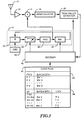
- FIG 1 shows a paging receiver operating in accordance with the present invention.
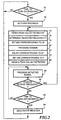
- FIG 2 shows a flow chart of a decoder operating in accordance with the present invention.
- FIG. 1 shows a paging receiver operating in accordance with the present invention.
- RF modulated paging signals are received on antenna 10, amplified by amplifier 12 mixed by mixer 14 with an injection frequency from synthesizer 16 in order to create an intermediate frequency signal.
- Demodulator 18 generates an audio signal from the intermediate frequency signal.
- the audio signal is digitized by the peak and valley detector 20 which generates a digital signal from the audio signal. Peak and valley detector 20 is described in U.S. patent 4,631,737 to Davis et al.
- Synthesizer 16 comprises a phase lock loop (PLL) and is driven by a reference frequency from oscillator 22.
- the reference frequency is compared by phase comparator 24.
- the output of the phase comparator is filtered by a programmable loop filter 26 which is described in U.S. patent US-A-4 901 033 and assigned to the assignee of the present invention which provides for a variable filter characteristic.
- the output of the loop filter is coupled to voltage controlled oscillator 28 which generates the injection frequency.
- the injection frequency is further coupled to programmable divider 30 the output of which is coupled to phase comparator 24, thus closing the loop of the PLL.
- Decoder 40 receives and processes the digitized signal from peak and valley detector 20 and also enables and disables the peak and valley detector. Programmable filter 26 and programmable divider 30 are also programmed by decoder 40. Decoder 40 includes a microcomputer for performing its functions. Use of a microcomputer or control functions of a paging receiver is known in the art. A preferred microcomputer is the MC68HC05C4 microcomputer manufactured by Motorola Inc. Some elements of the invention described herein are implemented in software operating within the microcomputer.
- Codeplug 50 includes several variables used to vary the characteristics of the receiver in response to the receive frequency.
- a first portion 52 contains frequency information and corresponding loop bandwidth information.
- a second portion contains the change in frequency information, AF and corresponding bandwidth and lock time information.
- table 52 for the paging receiver of this example could read:
- Table 54 governs the loop bandwidth during lock acquisition and table 54 further governs the lock time provided by the decoder. A relationship exists between the loop bandwidth and the lock time. The relationship is characterized and stored in the codeplug for use by the decoder. The following example uses the above frequencies for table 54.
- a 330 Hz bandwidth is used for the loop filter.
- the fourth and fifth rows show changing the bandwidth in order to provide for faster or slower lock times respectively. These rows may be used in response to commands within the paging signal causing the pager to switch from F1 to F2.
- the final three rows show starting from a starting frequency FS and bandwidth required to lock on to F1 through F3 respectively in 10 mS.
- the starting frequency, FS is indicative of the free running frequency of the VCO when it is initially powered on. Thus these rows are used when power is initially applied to the receiver which corresponds to the pager being brought out of the battery saving state.
- FIG. 2 shows a flowchart of a decoder operating in accordance with the present invention.
- the flowchart begins in step 70 with the receiver in the battery save state, thereby disabled.
- Step 70 is executed until it is time to turn the receiver on.
- step 72 the receiver is activated or turned on, thereby exiting the battery saving state.
- step 74 the peak valley detector is reset.
- Step 76 determines the receiver frequency which may be made by one of several known algorithms. One such algorithm is shown in U.S. patent 4,644,347 Feb. 17, 1987 to Lucas et al.
- Step 78 determines the loop bandwidth with which to program loop filter 30.
- the decoder selects the bandwidth corresponding to FS-F3 from the table above (570 Hz).
- the divider 30 is then programmed in order to receive frequency F3.
- a delay is executed by the software as determined by the FS-F3 lock time entry in the codeplug (10mS from the above table).
- the bandwidth of the loop filter 26 is changed to correspond to the desired bandwidth of frequency F3 (120 Hz from the table above).
- the peak and valley detector 20 is enabled.
- step 88 the decoder processes the detected signal.
- Step 90 checks if the frequency is to be changed, which could be in response to a signal received by the receiver. If the frequency is not to be changed, step 92 checks if it is time to turn off the receiver, a decision which may be made after completing reception of a paging signal. If it is not time to turn the receiver off, step 80 is returned to and signal processing continues. If it is time to turn the receiver off, step 94 deactivates the receiver thereby entering the battery save mode and step 70 is executed.
- step 74 would be executed.
- the peak and valley detector would be reset and the next frequency would be determined. If for example, the pager was in the scanning mode, currently receiving F3, and F1 was the next frequency to be scanned, information from the F3-F1 row of the above table would be used in steps 78-86. If for example, the receiver was receiving F1 and detected a paging signal directing the pager to rapidly switch to F2, the receiver would use the 5mS lock time setting from the F1-F2 row of the table above in steps 78-86.
- the programmable loop filter draws higher current when operating in the wider bandwidth, so it is generally desirable to use narrower bandwidths when possible. Furthermore, narrower bandwidths provides for reduced phase noise which may be desirable.
Landscapes
- Engineering & Computer Science (AREA)
- Computer Hardware Design (AREA)
- Microelectronics & Electronic Packaging (AREA)
- Mobile Radio Communication Systems (AREA)
- Superheterodyne Receivers (AREA)
- Circuits Of Receivers In General (AREA)
- Input Circuits Of Receivers And Coupling Of Receivers And Audio Equipment (AREA)
- Stabilization Of Oscillater, Synchronisation, Frequency Synthesizers (AREA)
Claims (7)
- Ein Funkrufempfänger (10-50), der einen Dekodierer (40) umfaßt, der mit einem Synthesizer (16) gekoppelt ist, der einen programmierbaren Phasenregelkreis (22-30) aufweist, der angeordnet ist, ein empfangenes Signal einer ersten Frequenz zu demodulieren, wobei der Funkrufempfänger umfaßt:eine Bestimmungseinrichtung zum Bestimmen einer Differenz zwischen der ersten Frequenz und einer Anfangsfrequenz des Synthesizers (16), wobei die Bestimmungseinrichtung ein Differenzsignal in Reaktion darauf erzeugt; undeine Speichereinrichtung (50) zum Speichern einer Mehrzahl von Delta-Bandbreitensignalen (52), von denen jedes einem jeweiligen Differenzsignal entspricht und verwendet wird, unter einer Mehrzahl von auswählbaren Eigenschaften für den Funkrufempfänger auszuwählen;worin der Phasenregelkreis PLL (22-30) ein Schleifenfilter (26) enthält, das eine Mehrzahl von auswählbaren Bandbreiten (BB) aufweist, unter denen eine in Reaktion auf ein bestimmtes Delta-Bandbreitensignal auswählbar ist, und worin der Dekodierer (40) angeordnet ist, eines der Delta-Bandbreitensignale (52), die in der Speichereinrichtung (50) gespeichert sind, entsprechend dem Differenzsignal auszuwählen, das durch die Bestimmungseinrichtung erzeugt wird.
- Der Funkrufempfänger des Anspruchs 1, worin die Speichereinrichtung (50) des weiteren mindestens ein Sperrzeitverzögerungssignal (54) speichert, und der Funkrufempfänger des weiteren umfaßt:
eine Verzögerungseinrichtung (54) zum Initiieren einer zeitlich festlegten Verzögerung in Reaktion auf den Dekodierer (40), der eine der Mehrzahl auswählbarer Eigenschaften auswählt, worin die zeitlich festgelegte Verzögerung eine Zeitdauer hat, die einem des wenigstens einen Sperrzeitverzögerungssignal entspricht, das mit dem Differenzsignal verbunden ist. - Der Funkrufempfänger des Anspruchs 2, des weiteren umfassend:
eine Einrichtung zum Erzeugen eines Vollendungssignals in Reaktion auf den Abschluß der zeitlich festgelegten Verzögerung, worin der Dekodierer (40) in Reaktion auf das Vollendungssignal eine der Mehrzahl von auswählbaren Eigenschaften auswählt, die eine Bandbreite des Schleifenfilters hat, die für das empfangene Signal der ersten Frequenz geeignet ist. - Der Funkrufempfänger des Anspruchs 3, worin das demodulierte, empfangene Signal Gleichstrom- und Wechselstromkomponenten hat, und worin der Funkrufempfänger des weiteren umfaßt:
eine Einrichtung (20) zum Bestimmen und Entfernen der Gleichstromkomponente und zum Digitalisieren der Wechselstromkomponente zur Verarbeitung durch den Dekodierer (40), worin die Einrichtung (20) zum Bestimmen, Entfernen und Digitalisieren in Reaktion auf das Vollendungssignal freigegeben wird. - Ein Verfahren zur Steuerung eines Funkrufempfänger (10-50), der Synthesizer (16) umfaßt, der einen programmierbaren Phasenregelkreis (22-30) aufweist, der angeordnet ist, ein empfangenes Signal einer ersten Frequenz zu demodulieren, wobei der Phasenregelkreis ein Schleifenfilter (26) einschließt, wobei das Verfahren die Schritte umfaßt:Bestimmen einer Differenz zwischen der ersten Frequenz und einer Anfangsfrequenz des Synthesizers (16), und Erzeugen eines Differenzsignals in Reaktion darauf;Speichern einer Mehrzahl von Variablen in einem Speicher, die auswählbare Eigenschaften des Funkrufempfängers darstellen, wobei die Variablen eine Mehrzahl von Delta-Bandbreitensignalen (52) umfassen, von denen jedes einem jeweiligen Differenzsignal entspricht, und einer Mehrzahl von auswählbaren Bandbreiten (BB) zum Steuern der Empfindlichkeit des Schleifenfilters (26);Auswählen einer der Mehrzahl von auswählbaren Eigenschaften in Reaktion auf das genannte erzeugte Differenzsignal, so daß der Funkrufempfänger das empfangene Signal demoduliert.
- Das Verfahren gemäß Anspruch 6, das ferner die Schritte umfaßt:Speichern eines Sperrzeitverzögerungssignals, das mit dem Differenzsignal verbunden ist;Initiieren einer zeitlich festgelegten Verzögerung, die eine Zeitdauer hat, die dem Sperrzeitverzögerungssignal entspricht;Erzeugen eines Vollendungssignals in Reaktion auf den Ab-schluß der zeitlich festgelegten Verzögerung; undAuswählen einer der Mehrzahl von auswählbaren Eigenschaften mit einer Bandbreite für das Schleifenfilter, die für das empfangene Signal der ersten Frequenz geeignet ist.
- Das Verfahren gemäß Anspruch 5 oder 6, worin das empfangene Signal eine Wechselstromkomponente hat, und das Verfahren ferner die Schritte umfaßt:
Digitalisieren der Wechselstromkomponente, um ein digitales Signal zu erzeugen, wobei das digitale Signal die HF-modulierten Informationen umfaßt.
Applications Claiming Priority (3)
| Application Number | Priority Date | Filing Date | Title |
|---|---|---|---|
| US38845989A | 1989-08-02 | 1989-08-02 | |
| US388459 | 1989-08-02 | ||
| PCT/US1990/003791 WO1991002418A1 (en) | 1989-08-02 | 1990-07-09 | Synthesized selective call receiver having variable characteristics |
Publications (3)
| Publication Number | Publication Date |
|---|---|
| EP0487548A1 EP0487548A1 (de) | 1992-06-03 |
| EP0487548A4 EP0487548A4 (en) | 1992-12-16 |
| EP0487548B1 true EP0487548B1 (de) | 1997-03-05 |
Family
ID=23534199
Family Applications (1)
| Application Number | Title | Priority Date | Filing Date |
|---|---|---|---|
| EP90911065A Expired - Lifetime EP0487548B1 (de) | 1989-08-02 | 1990-07-09 | Funkrufempfänger mit synthesizer mit veränderbaren eigenschaften |
Country Status (8)
| Country | Link |
|---|---|
| EP (1) | EP0487548B1 (de) |
| JP (1) | JP2557284B2 (de) |
| KR (1) | KR950013308B1 (de) |
| AT (1) | ATE149764T1 (de) |
| CA (1) | CA2057013C (de) |
| DE (1) | DE69030091T2 (de) |
| SG (1) | SG44534A1 (de) |
| WO (1) | WO1991002418A1 (de) |
Families Citing this family (3)
| Publication number | Priority date | Publication date | Assignee | Title |
|---|---|---|---|---|
| FR2726724B1 (fr) * | 1994-11-07 | 1997-01-10 | Motorola Inc | Dispositif et procede pour le fonctionnement d'un synthetiseur en frequence de boucle a blocage de phase sensible a l'espacement de canal de frequence radio |
| FI950106L (fi) * | 1995-01-10 | 1996-07-11 | Nokia Mobile Phones Ltd | Menetelmä ja kytkentä häiriöiden suodattamiseksi radiolaitteen vastaanottimessa |
| GB2336731A (en) * | 1998-04-22 | 1999-10-27 | Thomson Multimedia Sa | A video tuner in which data representing a PLL division is used to control other circuit parameters |
Family Cites Families (2)
| Publication number | Priority date | Publication date | Assignee | Title |
|---|---|---|---|---|
| JPS5828968B2 (ja) * | 1977-08-31 | 1983-06-20 | ソニー株式会社 | Pll方式周波数シンセサイザチュ−ナ |
| US4259740A (en) * | 1979-03-07 | 1981-03-31 | Harris Corporation | Sequential detection system |
-
1990
- 1990-07-09 CA CA002057013A patent/CA2057013C/en not_active Expired - Fee Related
- 1990-07-09 SG SG1996001684A patent/SG44534A1/en unknown
- 1990-07-09 EP EP90911065A patent/EP0487548B1/de not_active Expired - Lifetime
- 1990-07-09 AT AT90911065T patent/ATE149764T1/de not_active IP Right Cessation
- 1990-07-09 JP JP2510459A patent/JP2557284B2/ja not_active Expired - Lifetime
- 1990-07-09 KR KR1019920700204A patent/KR950013308B1/ko not_active Expired - Lifetime
- 1990-07-09 DE DE69030091T patent/DE69030091T2/de not_active Expired - Fee Related
- 1990-07-09 WO PCT/US1990/003791 patent/WO1991002418A1/en not_active Ceased
Also Published As
| Publication number | Publication date |
|---|---|
| DE69030091T2 (de) | 1997-09-18 |
| DE69030091D1 (de) | 1997-04-10 |
| CA2057013A1 (en) | 1991-02-03 |
| JPH04507330A (ja) | 1992-12-17 |
| JP2557284B2 (ja) | 1996-11-27 |
| EP0487548A4 (en) | 1992-12-16 |
| EP0487548A1 (de) | 1992-06-03 |
| KR950013308B1 (ko) | 1995-11-02 |
| ATE149764T1 (de) | 1997-03-15 |
| SG44534A1 (en) | 1997-12-19 |
| WO1991002418A1 (en) | 1991-02-21 |
| CA2057013C (en) | 1995-01-17 |
Similar Documents
| Publication | Publication Date | Title |
|---|---|---|
| US5058204A (en) | Synthesized selective call receiver having variable characteristics | |
| CA1066781A (en) | Universal automotive electronic radio | |
| US4685150A (en) | Tuning of a resonant circuit in a communications receiver | |
| US4654884A (en) | Radio receiver with switching circuit for elimination of intermodulation interference | |
| EP0372430B1 (de) | Selbsttätige Antennenabstimmung | |
| US6731349B1 (en) | Tuner with at least a first and a second frequency band | |
| HK1002048B (en) | Automatic antenna tuning | |
| US5438688A (en) | Channel selecting method and highspeed scanning radio receiver which concurrently scans multiple channels | |
| KR830002629B1 (ko) | 전자식 동조장치 | |
| JP2625759B2 (ja) | オートチューニング装置 | |
| EP0487548B1 (de) | Funkrufempfänger mit synthesizer mit veränderbaren eigenschaften | |
| US20010026597A1 (en) | Synthesizer receiver | |
| US4989263A (en) | Radio receiver with automatic mode changeover circuit | |
| JP2770973B2 (ja) | ラジオ受信機のオートプリセット装置 | |
| JPH02108320A (ja) | オートスキャンチューナ | |
| US3987399A (en) | Radio receiver | |
| JP2541204B2 (ja) | オ−トチユ−ニング装置 | |
| KR900008163B1 (ko) | 소인(掃印)선국장치의 자동정지회로 | |
| JP3070987B2 (ja) | 自動選局回路 | |
| KR20010000999A (ko) | 티브이의 채널 탐색속도와 탐색레벨에 따른 자동채널 설정장치 및 방법 | |
| JPH03187612A (ja) | チューナ | |
| JP2806475B2 (ja) | ラジオ受信機 | |
| JP2561352B2 (ja) | 自動同調受信機 | |
| JP2541202B2 (ja) | オ−トチユ−ニング装置 | |
| JPS5857927B2 (ja) | 自動同調ラジオ |
Legal Events
| Date | Code | Title | Description |
|---|---|---|---|
| PUAI | Public reference made under article 153(3) epc to a published international application that has entered the european phase |
Free format text: ORIGINAL CODE: 0009012 |
|
| 17P | Request for examination filed |
Effective date: 19920218 |
|
| AK | Designated contracting states |
Kind code of ref document: A1 Designated state(s): AT BE CH DE DK ES FR GB IT LI LU NL SE |
|
| A4 | Supplementary search report drawn up and despatched |
Effective date: 19921005 |
|
| AK | Designated contracting states |
Kind code of ref document: A4 Designated state(s): AT BE CH DE DK ES FR GB IT LI LU NL SE |
|
| 17Q | First examination report despatched |
Effective date: 19940928 |
|
| GRAG | Despatch of communication of intention to grant |
Free format text: ORIGINAL CODE: EPIDOS AGRA |
|
| GRAH | Despatch of communication of intention to grant a patent |
Free format text: ORIGINAL CODE: EPIDOS IGRA |
|
| GRAH | Despatch of communication of intention to grant a patent |
Free format text: ORIGINAL CODE: EPIDOS IGRA |
|
| GRAA | (expected) grant |
Free format text: ORIGINAL CODE: 0009210 |
|
| ITF | It: translation for a ep patent filed | ||
| AK | Designated contracting states |
Kind code of ref document: B1 Designated state(s): AT BE CH DE DK ES FR GB IT LI LU NL SE |
|
| PG25 | Lapsed in a contracting state [announced via postgrant information from national office to epo] |
Ref country code: NL Free format text: LAPSE BECAUSE OF FAILURE TO SUBMIT A TRANSLATION OF THE DESCRIPTION OR TO PAY THE FEE WITHIN THE PRESCRIBED TIME-LIMIT Effective date: 19970305 Ref country code: LI Effective date: 19970305 Ref country code: ES Free format text: THE PATENT HAS BEEN ANNULLED BY A DECISION OF A NATIONAL AUTHORITY Effective date: 19970305 Ref country code: DK Effective date: 19970305 Ref country code: CH Effective date: 19970305 Ref country code: BE Effective date: 19970305 Ref country code: AT Effective date: 19970305 |
|
| REF | Corresponds to: |
Ref document number: 149764 Country of ref document: AT Date of ref document: 19970315 Kind code of ref document: T |
|
| ET | Fr: translation filed | ||
| REG | Reference to a national code |
Ref country code: CH Ref legal event code: EP |
|
| REF | Corresponds to: |
Ref document number: 69030091 Country of ref document: DE Date of ref document: 19970410 |
|
| ET | Fr: translation filed |
Free format text: CORRECTIONS |
|
| PG25 | Lapsed in a contracting state [announced via postgrant information from national office to epo] |
Ref country code: SE Effective date: 19970605 |
|
| PG25 | Lapsed in a contracting state [announced via postgrant information from national office to epo] |
Ref country code: LU Free format text: LAPSE BECAUSE OF NON-PAYMENT OF DUE FEES Effective date: 19970709 |
|
| NLV1 | Nl: lapsed or annulled due to failure to fulfill the requirements of art. 29p and 29m of the patents act | ||
| REG | Reference to a national code |
Ref country code: CH Ref legal event code: PL |
|
| PLBE | No opposition filed within time limit |
Free format text: ORIGINAL CODE: 0009261 |
|
| STAA | Information on the status of an ep patent application or granted ep patent |
Free format text: STATUS: NO OPPOSITION FILED WITHIN TIME LIMIT |
|
| 26N | No opposition filed | ||
| REG | Reference to a national code |
Ref country code: GB Ref legal event code: IF02 |
|
| PGFP | Annual fee paid to national office [announced via postgrant information from national office to epo] |
Ref country code: GB Payment date: 20030612 Year of fee payment: 14 |
|
| PGFP | Annual fee paid to national office [announced via postgrant information from national office to epo] |
Ref country code: FR Payment date: 20030702 Year of fee payment: 14 |
|
| PGFP | Annual fee paid to national office [announced via postgrant information from national office to epo] |
Ref country code: DE Payment date: 20030731 Year of fee payment: 14 |
|
| PG25 | Lapsed in a contracting state [announced via postgrant information from national office to epo] |
Ref country code: GB Free format text: LAPSE BECAUSE OF NON-PAYMENT OF DUE FEES Effective date: 20040709 |
|
| PG25 | Lapsed in a contracting state [announced via postgrant information from national office to epo] |
Ref country code: DE Free format text: LAPSE BECAUSE OF NON-PAYMENT OF DUE FEES Effective date: 20050201 |
|
| GBPC | Gb: european patent ceased through non-payment of renewal fee |
Effective date: 20040709 |
|
| PG25 | Lapsed in a contracting state [announced via postgrant information from national office to epo] |
Ref country code: FR Free format text: LAPSE BECAUSE OF NON-PAYMENT OF DUE FEES Effective date: 20050331 |
|
| REG | Reference to a national code |
Ref country code: FR Ref legal event code: ST |
|
| PG25 | Lapsed in a contracting state [announced via postgrant information from national office to epo] |
Ref country code: IT Free format text: LAPSE BECAUSE OF NON-PAYMENT OF DUE FEES;WARNING: LAPSES OF ITALIAN PATENTS WITH EFFECTIVE DATE BEFORE 2007 MAY HAVE OCCURRED AT ANY TIME BEFORE 2007. THE CORRECT EFFECTIVE DATE MAY BE DIFFERENT FROM THE ONE RECORDED. Effective date: 20050709 |
|
| P01 | Opt-out of the competence of the unified patent court (upc) registered |
Effective date: 20230522 |