EP0488211A2 - Dispositif optique independent de la polarisation - Google Patents
Dispositif optique independent de la polarisation Download PDFInfo
- Publication number
- EP0488211A2 EP0488211A2 EP91120270A EP91120270A EP0488211A2 EP 0488211 A2 EP0488211 A2 EP 0488211A2 EP 91120270 A EP91120270 A EP 91120270A EP 91120270 A EP91120270 A EP 91120270A EP 0488211 A2 EP0488211 A2 EP 0488211A2
- Authority
- EP
- European Patent Office
- Prior art keywords
- layer film
- dielectric multi
- beam splitter
- tapered
- optical device
- Prior art date
- Legal status (The legal status is an assumption and is not a legal conclusion. Google has not performed a legal analysis and makes no representation as to the accuracy of the status listed.)
- Granted
Links
Images



Classifications
-
- G—PHYSICS
- G02—OPTICS
- G02B—OPTICAL ELEMENTS, SYSTEMS OR APPARATUS
- G02B6/00—Light guides; Structural details of arrangements comprising light guides and other optical elements, e.g. couplings
- G02B6/24—Coupling light guides
- G02B6/26—Optical coupling means
- G02B6/27—Optical coupling means with polarisation selective and adjusting means
- G02B6/2746—Optical coupling means with polarisation selective and adjusting means comprising non-reciprocal devices, e.g. isolators, FRM, circulators, quasi-isolators
-
- G—PHYSICS
- G02—OPTICS
- G02B—OPTICAL ELEMENTS, SYSTEMS OR APPARATUS
- G02B1/00—Optical elements characterised by the material of which they are made; Optical coatings for optical elements
- G02B1/10—Optical coatings produced by application to, or surface treatment of, optical elements
-
- G—PHYSICS
- G02—OPTICS
- G02B—OPTICAL ELEMENTS, SYSTEMS OR APPARATUS
- G02B27/00—Optical systems or apparatus not provided for by any of the groups G02B1/00 - G02B26/00, G02B30/00
- G02B27/28—Optical systems or apparatus not provided for by any of the groups G02B1/00 - G02B26/00, G02B30/00 for polarising
- G02B27/283—Optical systems or apparatus not provided for by any of the groups G02B1/00 - G02B26/00, G02B30/00 for polarising used for beam splitting or combining
-
- G—PHYSICS
- G02—OPTICS
- G02B—OPTICAL ELEMENTS, SYSTEMS OR APPARATUS
- G02B5/00—Optical elements other than lenses
- G02B5/30—Polarising elements
- G02B5/3083—Birefringent or phase retarding elements
Definitions
- the present invention relates to a polarization independent optical device such as, for example, an optical coupler or an optical multiplexer/demultiplexer.
- an optical device for an optical communication system e.g. an optical multiplexer/demultiplexer or an optical coupler, constituted by a prism having a dielectric multi-layer film
- the angle of incidence of light beam on the dielectric multi-layer film is as large as 20° to 45°
- the polarization dependence of the dielectric multi-layer film is high and so the characteristics of the optical multiplexer/demultiplexer or the optical coupler are unstable.
- Such polarization dependence of the dielectric multi-layer film restricts the design of an optical path in the optical device because a semiconductor laser having polarizability is used mainly as a light source for the optical communication system, and for eliminating this inconvenience, the development of an optical device with a polarization independent dielectric multi-layer film has been pursued.
- Fig. 1 is a plan view of a conventional optical coupler assembly.
- Four fiber lens assemblies 4a, 4b, 4c and 4d are mounted to a housing 2.
- a glass substrate 6 Within the housing 2 is disposed a glass substrate 6.
- a coupler film 8 constituted by a dielectric multi-layer film and a non-reflective film 10 are stuck on the glass substrate 6.
- the angle of incidence, ⁇ , on the coupler film 8 from each of the fiber lens assemblies 4a - 4d is set at a value not larger than 15° at which the polarization dependence of the coupler film 8 is not so high.
- light beam emitted from the fiber lens assembly 4a is splitted at a predetermined split ratio by the coupler film 8 and then coupled to the fiber lens assemblies 4b and 4c.
- Light beam from the fiber lens assembly 4b is splitted at a predetermined split ratio by the coupler film 8 and then the coupled to the fiber lens assemblies 4a and 4d. In this way, light beam from the fiber lens assembly 4c or 4d is also splitted and coupled.
- the angle of incidence of light beam on the same film has been kept to a value not larger than about 15° in constituting an optical device.
- a polarization independent optical device comprising a tapered double-refractive crystal disposed so that an optic axis thereof is perpendicular to an incident optical path, and a dielectric multi-layer film disposed on an exit side of light beam with respect to the tapered double-refractive crystal.
- said optical device includes a 1/2 wavelength plate having an optic axis inclined 22.5° relative to a vibrating direction of P- or S-wave of the dielectric multi-layer film, provided on the light beam exit side with respect to the dielectric multi-layer film.
- a polarization independent optical device comprising a cubic beam splitter including first and second rectangular prisms each having a slant face, and a dielectric multi-layer film formed in an interface between the first and second rectangular prisms which are stuck together at the respective slant faces, an incidence-side surface of the cubic beam splitter being inclined at a predetermined angle relative to an incident optical path; and a tapered double-refractive crystal stuck on the incidence-side surface of the cubic beam splitter and having an optic axis perpendicular to the incident optical path.
- a polarization independent optical device comprising a beam splitter having a dielectric multi-layer film; and an optical isolator disposed on a light beam incidence side with respect to the said beam splitter and including a polarizer, an optical rotator and an analyzer, the analyzer of the optical isolator having a transmitting polarization plane inclined 45° from vibrating directions of P- and S-waves of the dielectric multi-layer film.
- incident light beam can be brought into a non-polarized state by passing it through the tapered double-refractive crystal and hence the polarization dependence of the dielectric multi-layer film can be eliminated on the surface.
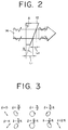
- the reference numeral 12 denotes a double-refractive crystal, e.g. quartz, having a taper angle ⁇ of approximately 2° or smaller, which crystal is disposed in such a manner that an optic axis A thereof is perpendicular to an optical path of a light beam 14.
- the mark L2 in Fig. 2 represents a phase difference generating optical path length for a single light of ordinary or extraordinary light because of a finite diameter of the light beam 14.
- Fig. 3 shows variations of polarization according to phase difference ⁇ .
- phase difference ⁇ When the phase difference is 0, a linearly polarized light beam is obtained. The light beam changes into an eliptically polarized light beam and then a circularly polarized light beam as the phase difference increases. And when the phase difference ⁇ becomes 2 ⁇ , the polarization reverts to the original linear polarization.
- Fig. 4 is a plan view of an optical coupler according to a first embodiment of the present invention.
- a tapered glass plate 20 and a tapered quartz plate 22 having an optic axis perpendicular to an incident optic path are stuck together to form a parallel flat substrate 26, and a coupler film 24 formed of a dielectric multi-layer film is vapor-deposited on the back of the tapered quartz plate 22.
- Incident light is brought into a non-polarized state by passing through the tapered quartz plate 22 of the substrate 26, and then impinges on the coupler film 24. Therefore, even if the angle of incidence is set at a large value of 45° or so, there does not occur a polarization dependence of the coupler film 24.
- the beam diameter is 1 mm and the taper angle of the tapered quartz plate 22 is 0.5°
- a phase difference of at least 5 ⁇ relative to a linearly polarized light is obtained between both ends of beam.
- the optic axis of the tapered quartz plate 22 is set perpendicularly to the incident optical path and is inclined 45° relative to the vibrating direction of P- or S- wave of the coupler film 24, whereby P- and S-wave components for the coupler film 24 of the light emitted from the tapered quartz plate 22 can be made equal in ratio, and hence it is possible to eliminate the apparent polarization dependence of the coupler film 24 completely.
- Fig. 5 is a plan view of an optical coupler according to a second embodiment of the present invention.
- the parallel flat substrates 26 each with the coupler film 24 vapor-deposited thereon, shown in Fig. 4 are disposed in two stages to split light beam in two stages.
- a tapered quartz plate 22 In front of each coupler film 24 there is disposed a tapered quartz plate 22. This is because even if a non-polarized state is once obtained by the tapered quartz plate 22 of the first stage, a slight polarization is induced in reflected light and transmitted light due to the polarization dependence of the coupler film 24, so it is necessary to attain a non-polarized state in each stage.
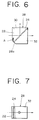
- Fig. 6 is a plan view of a third embodiment of the present invention and Fig. 7 is a side view thereof.
- a coupler film 24 formed of a dielectric multi-layer film is sandwiched between two rectangular prisms 30 and 32 to form a cubic beam splitter 28.
- the beam splitter 28 has an incidence-side surface inclined by a predetermined angle, and a tapered quartz plate 22 having an optic axis A perpendicular to an incident optical path is stuck on the incidence-side surface.
- the beam splitter 28 is constructed so that its incidence-and exit-side surfaces are parallel to each other to prevent deflection of the optical path. Further, for ease of production, a cutout portion 28a is formed at one corner of the beam splitter 28.
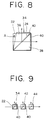
- Fig. 8 is a plan view of a fourth embodiment of the present invention.
- a coupler film 24 formed of a dielectric multi-layer film is sandwiched between two rectangular prisms 36 and 40 to form a cubic beam splitter 34.
- a tapered quartz plate 22 having an optic axis A perpendicular to an incident optical path is stuck on an incidence-side surface of the cubic beam splitter 34, while 1/2 wavelength plates 40 each having an optic axis inclined 22.5° relative to a vibrating direction of P- or S-wave of the coupler film 24 are stuck on exit-side surfaces of the beam splitter 34.
- Fig. 9 is a plan view of a fifth embodiment of the present invention in which light beam is splitted in three stages.
- a beam splitter 34 with both a tapered quartz plate 22 and a 1/2 wavelength plate 40 stuck thereon, a beam splitter 42 with only a 1/2 wavelength plate stuck thereon, and an ordinary beam splitter 44, are arranged in series in an optical path of light beam, whereby the polarization dependence can be eliminated with respect to all of coupler films.
- Fig. 10 is a construction diagram of a sixth embodiment of the present invention, in which the reference numeral 50 denotes an optical isolator comprising a polarized beam splitter (polarizer) 52, a YIG crystal 54, a 1/2 wavelength plate 56 and a polarized beam splitter (analyzer) 58.
- polarizer polarized beam splitter
- YIG crystal 54 a YIG crystal 54
- 1/2 wavelength plate 56 a polarized beam splitter
- analyzer polarized beam splitter
- P- and S-wave components for the coupler film 62 of the light emitted from the optical isolator 50 can be made equal in ratio, so that the apparent polarization dependence of the coupler film 62 can be eliminated.
Landscapes
- Physics & Mathematics (AREA)
- General Physics & Mathematics (AREA)
- Optics & Photonics (AREA)
- Polarising Elements (AREA)
Applications Claiming Priority (2)
| Application Number | Priority Date | Filing Date | Title |
|---|---|---|---|
| JP2320769A JPH04191703A (ja) | 1990-11-27 | 1990-11-27 | 偏光無依存性光学部品 |
| JP320769/90 | 1990-11-27 |
Publications (3)
| Publication Number | Publication Date |
|---|---|
| EP0488211A2 true EP0488211A2 (fr) | 1992-06-03 |
| EP0488211A3 EP0488211A3 (en) | 1993-05-26 |
| EP0488211B1 EP0488211B1 (fr) | 1998-02-04 |
Family
ID=18125054
Family Applications (1)
| Application Number | Title | Priority Date | Filing Date |
|---|---|---|---|
| EP91120270A Expired - Lifetime EP0488211B1 (fr) | 1990-11-27 | 1991-11-27 | Dispositif optique independent de la polarisation |
Country Status (5)
| Country | Link |
|---|---|
| US (2) | US5377040A (fr) |
| EP (1) | EP0488211B1 (fr) |
| JP (1) | JPH04191703A (fr) |
| CA (1) | CA2056130A1 (fr) |
| DE (1) | DE69128872T2 (fr) |
Cited By (2)
| Publication number | Priority date | Publication date | Assignee | Title |
|---|---|---|---|---|
| EP1059543A1 (fr) * | 1999-05-12 | 2000-12-13 | Hewlett-Packard Company | Appareil de mesure avec une interface optique ayant des faibles pertes dépendant de la polarisation |
| WO2004063777A1 (fr) * | 2003-01-16 | 2004-07-29 | Carl Zeiss Smt Ag | Lame de retard |
Families Citing this family (11)
| Publication number | Priority date | Publication date | Assignee | Title |
|---|---|---|---|---|
| JPH04191703A (ja) * | 1990-11-27 | 1992-07-10 | Fujitsu Ltd | 偏光無依存性光学部品 |
| US5400179A (en) * | 1992-02-18 | 1995-03-21 | Asahi Kogaku Kogyo Kabushiki Kaisha | Optical multilayer thin film and beam splitter |
| US5539574A (en) * | 1994-12-21 | 1996-07-23 | At&T Corp. | Optical isolator with fabry-perot ripple reduction |
| US5808798A (en) * | 1996-03-27 | 1998-09-15 | Minnesota Mining And Manufacturing Co. | Nonpolarizing beamsplitter |
| JP3884857B2 (ja) * | 1998-03-12 | 2007-02-21 | 富士通株式会社 | 偏光合成装置および偏光分離装置 |
| JP2003015085A (ja) * | 2001-06-28 | 2003-01-15 | Ando Electric Co Ltd | 偏光解消板および分光器 |
| GB2442650A (en) * | 2005-07-12 | 2008-04-09 | Gsi Group Corp | System and method for high power laser processing |
| DE102007055567A1 (de) | 2007-11-20 | 2009-05-28 | Carl Zeiss Smt Ag | Optisches System |
| US7876496B2 (en) * | 2008-05-23 | 2011-01-25 | Photop Technologies, Inc. | Free-space optical module for optical amplification |
| DE102010033427A1 (de) * | 2010-08-04 | 2012-02-09 | Karl Storz Gmbh & Co. Kg | Endoskop mit einstellbarer Blickrichtung |
| JP5751328B2 (ja) * | 2011-06-29 | 2015-07-22 | 株式会社ニコン | 構造化照明光学系および構造化照明顕微鏡装置 |
Family Cites Families (24)
| Publication number | Priority date | Publication date | Assignee | Title |
|---|---|---|---|---|
| US1926716A (en) * | 1930-11-03 | 1933-09-12 | Firm R Winkel G M B H | Double refraction device |
| US3511556A (en) * | 1967-11-30 | 1970-05-12 | Sylvania Electric Prod | Optical polarizing prism |
| GB1330836A (en) * | 1969-11-24 | 1973-09-19 | Vickers Ltd | Optical field-flattening devices |
| SE7502770L (fr) * | 1974-03-12 | 1975-09-15 | Comp Generale Electricite | |
| US3744876A (en) * | 1971-07-02 | 1973-07-10 | R Kay | Optical device for transformation of polarization |
| US4103260A (en) * | 1977-01-03 | 1978-07-25 | Hughes Aircraft Company | Spatial polarization coding electro-optical transmitter |
| US4198123A (en) * | 1977-03-23 | 1980-04-15 | Baxter Travenol Laboratories, Inc. | Optical scrambler for depolarizing light |
| JPS5588009A (en) * | 1978-12-26 | 1980-07-03 | Nippon Telegr & Teleph Corp <Ntt> | Double refractive polarizing prism |
| JPS56137307A (en) * | 1980-03-31 | 1981-10-27 | Mitsubishi Electric Corp | Optical branching filter |
| JPS5754906A (en) * | 1980-09-19 | 1982-04-01 | Ito Koken Kk | Polarization prism |
| DE3149615A1 (de) * | 1981-12-15 | 1983-07-21 | Licentia Patent-Verwaltungs-Gmbh, 6000 Frankfurt | Optisches signaluebertragungsverfahren und anordnung zur durchfuehrung des verfahrens |
| JPS58202409A (ja) * | 1982-02-04 | 1983-11-25 | Toyo Commun Equip Co Ltd | ビ−ム・パタ−ン整形機能を備へた偏光ビ−ム・スプリツタ |
| US4492436A (en) * | 1983-01-03 | 1985-01-08 | At&T Bell Laboratories | Polarization independent beam splitter |
| JPS59140420A (ja) * | 1983-02-01 | 1984-08-11 | Canon Inc | 半導体レ−ザ−を用いた光源装置 |
| US4565426A (en) * | 1983-05-02 | 1986-01-21 | Cullen Ralph A W | Beam splitter |
| JPS59228610A (ja) * | 1983-06-10 | 1984-12-22 | Fuji Elelctrochem Co Ltd | 偏光プリズム |
| US4595261A (en) * | 1983-10-13 | 1986-06-17 | International Business Machines Corporation | Phase retardation element and prism for use in an optical data storage system |
| JPS60159821A (ja) * | 1984-01-31 | 1985-08-21 | Hoya Corp | 光分岐結合器 |
| US4671613A (en) * | 1985-11-12 | 1987-06-09 | Gte Laboratories Inc. | Optical beam splitter prism |
| US4682340A (en) * | 1985-12-30 | 1987-07-21 | Gte Government Systems Corporation | Apparatus for and method of extracting an output beam from a laser system |
| JPH01241502A (ja) * | 1988-03-23 | 1989-09-26 | Namiki Precision Jewel Co Ltd | 光アイソレータ用偏光素子 |
| JPH0264917A (ja) * | 1988-08-30 | 1990-03-05 | Nhk Spring Co Ltd | 光磁気記録装置用光学ヘッド構造 |
| US5223975A (en) * | 1988-11-11 | 1993-06-29 | Fujitsu Limited | Polarization beam coupler including a splitter for producing an output monitor beam |
| JPH04191703A (ja) * | 1990-11-27 | 1992-07-10 | Fujitsu Ltd | 偏光無依存性光学部品 |
-
1990
- 1990-11-27 JP JP2320769A patent/JPH04191703A/ja active Pending
-
1991
- 1991-11-25 CA CA002056130A patent/CA2056130A1/fr not_active Abandoned
- 1991-11-27 EP EP91120270A patent/EP0488211B1/fr not_active Expired - Lifetime
- 1991-11-27 DE DE69128872T patent/DE69128872T2/de not_active Expired - Fee Related
- 1991-11-27 US US07/799,159 patent/US5377040A/en not_active Expired - Fee Related
-
1997
- 1997-03-14 US US08/818,033 patent/US5739951A/en not_active Expired - Fee Related
Cited By (3)
| Publication number | Priority date | Publication date | Assignee | Title |
|---|---|---|---|---|
| EP1059543A1 (fr) * | 1999-05-12 | 2000-12-13 | Hewlett-Packard Company | Appareil de mesure avec une interface optique ayant des faibles pertes dépendant de la polarisation |
| US6430338B1 (en) | 1999-05-12 | 2002-08-06 | Agilent Technologies, Inc. | Measuring device with an optical interface with low polarization dependent loss (PDL) |
| WO2004063777A1 (fr) * | 2003-01-16 | 2004-07-29 | Carl Zeiss Smt Ag | Lame de retard |
Also Published As
| Publication number | Publication date |
|---|---|
| DE69128872D1 (de) | 1998-03-12 |
| JPH04191703A (ja) | 1992-07-10 |
| CA2056130A1 (fr) | 1992-05-28 |
| EP0488211A3 (en) | 1993-05-26 |
| EP0488211B1 (fr) | 1998-02-04 |
| DE69128872T2 (de) | 1998-06-18 |
| US5739951A (en) | 1998-04-14 |
| US5377040A (en) | 1994-12-27 |
Similar Documents
| Publication | Publication Date | Title |
|---|---|---|
| US5682446A (en) | Polarization mode dispersion-free circulator | |
| EP0100178B1 (fr) | Elément de polarisation | |
| US5377040A (en) | Polarization independent optical device | |
| JPH02239219A (ja) | 液晶表示システム用照明系 | |
| GB2038022A (en) | Optical circulator | |
| GB2264181A (en) | Optical isolator | |
| EP0040033B1 (fr) | Prisme polariseur | |
| US5999313A (en) | Optical device having function of optical circulator | |
| US3463571A (en) | Total internal reflection deflector | |
| JP3161885B2 (ja) | 光アイソレーター | |
| JP2516463B2 (ja) | 偏光無依存型光アイソレ―タ | |
| JPS63262602A (ja) | 回折格子型光偏光板 | |
| JPH085977A (ja) | 可変波長液晶光フィルタ | |
| JPS6365419A (ja) | 光アイソレ−タ付半導体レ−ザ装置 | |
| JP3038942B2 (ja) | 複屈折回折格子型偏光子および光アイソレータ | |
| JPH0894969A (ja) | 光サーキュレータおよび光の制御方法 | |
| JPH06100732B2 (ja) | フアイバ形アイソレ−タ | |
| JPS6257012B2 (fr) | ||
| JPH06160775A (ja) | 光アイソレータ | |
| JP3492736B2 (ja) | 光アイソレータ | |
| JPH10186278A (ja) | 光サーキュレータ | |
| JP2977926B2 (ja) | 光サ−キュレ−タ | |
| JP2686453B2 (ja) | 光アイソレータ | |
| CN119596567A (zh) | 具有偏振选择功能的偏振分束装置 | |
| JPH0454929B2 (fr) |
Legal Events
| Date | Code | Title | Description |
|---|---|---|---|
| PUAI | Public reference made under article 153(3) epc to a published international application that has entered the european phase |
Free format text: ORIGINAL CODE: 0009012 |
|
| AK | Designated contracting states |
Kind code of ref document: A2 Designated state(s): DE FR GB |
|
| PUAL | Search report despatched |
Free format text: ORIGINAL CODE: 0009013 |
|
| AK | Designated contracting states |
Kind code of ref document: A3 Designated state(s): DE FR GB |
|
| 17P | Request for examination filed |
Effective date: 19930714 |
|
| 17Q | First examination report despatched |
Effective date: 19950621 |
|
| GRAG | Despatch of communication of intention to grant |
Free format text: ORIGINAL CODE: EPIDOS AGRA |
|
| GRAG | Despatch of communication of intention to grant |
Free format text: ORIGINAL CODE: EPIDOS AGRA |
|
| GRAH | Despatch of communication of intention to grant a patent |
Free format text: ORIGINAL CODE: EPIDOS IGRA |
|
| GRAH | Despatch of communication of intention to grant a patent |
Free format text: ORIGINAL CODE: EPIDOS IGRA |
|
| GRAA | (expected) grant |
Free format text: ORIGINAL CODE: 0009210 |
|
| AK | Designated contracting states |
Kind code of ref document: B1 Designated state(s): DE FR GB |
|
| REF | Corresponds to: |
Ref document number: 69128872 Country of ref document: DE Date of ref document: 19980312 |
|
| ET | Fr: translation filed | ||
| PLBE | No opposition filed within time limit |
Free format text: ORIGINAL CODE: 0009261 |
|
| STAA | Information on the status of an ep patent application or granted ep patent |
Free format text: STATUS: NO OPPOSITION FILED WITHIN TIME LIMIT |
|
| 26N | No opposition filed | ||
| PGFP | Annual fee paid to national office [announced via postgrant information from national office to epo] |
Ref country code: FR Payment date: 19991109 Year of fee payment: 9 |
|
| PGFP | Annual fee paid to national office [announced via postgrant information from national office to epo] |
Ref country code: GB Payment date: 19991124 Year of fee payment: 9 |
|
| PGFP | Annual fee paid to national office [announced via postgrant information from national office to epo] |
Ref country code: DE Payment date: 19991129 Year of fee payment: 9 |
|
| PG25 | Lapsed in a contracting state [announced via postgrant information from national office to epo] |
Ref country code: GB Free format text: LAPSE BECAUSE OF NON-PAYMENT OF DUE FEES Effective date: 20001127 |
|
| GBPC | Gb: european patent ceased through non-payment of renewal fee |
Effective date: 20001127 |
|
| PG25 | Lapsed in a contracting state [announced via postgrant information from national office to epo] |
Ref country code: FR Free format text: LAPSE BECAUSE OF NON-PAYMENT OF DUE FEES Effective date: 20010731 |
|
| PG25 | Lapsed in a contracting state [announced via postgrant information from national office to epo] |
Ref country code: DE Free format text: LAPSE BECAUSE OF NON-PAYMENT OF DUE FEES Effective date: 20010801 |
|
| REG | Reference to a national code |
Ref country code: FR Ref legal event code: ST |