EP0488326A2 - Méthode de commande pour un panneau d'affichage à plasma - Google Patents
Méthode de commande pour un panneau d'affichage à plasma Download PDFInfo
- Publication number
- EP0488326A2 EP0488326A2 EP91120450A EP91120450A EP0488326A2 EP 0488326 A2 EP0488326 A2 EP 0488326A2 EP 91120450 A EP91120450 A EP 91120450A EP 91120450 A EP91120450 A EP 91120450A EP 0488326 A2 EP0488326 A2 EP 0488326A2
- Authority
- EP
- European Patent Office
- Prior art keywords
- field
- sub
- time
- scanning
- display panel
- Prior art date
- Legal status (The legal status is an assumption and is not a legal conclusion. Google has not performed a legal analysis and makes no representation as to the accuracy of the status listed.)
- Granted
Links
Images



Classifications
-
- G—PHYSICS
- G09—EDUCATION; CRYPTOGRAPHY; DISPLAY; ADVERTISING; SEALS
- G09G—ARRANGEMENTS OR CIRCUITS FOR CONTROL OF INDICATING DEVICES USING STATIC MEANS TO PRESENT VARIABLE INFORMATION
- G09G3/00—Control arrangements or circuits, of interest only in connection with visual indicators other than cathode-ray tubes
- G09G3/20—Control arrangements or circuits, of interest only in connection with visual indicators other than cathode-ray tubes for presentation of an assembly of a number of characters, e.g. a page, by composing the assembly by combination of individual elements arranged in a matrix no fixed position being assigned to or needed to be assigned to the individual characters or partial characters
- G09G3/2007—Display of intermediate tones
- G09G3/2018—Display of intermediate tones by time modulation using two or more time intervals
- G09G3/2022—Display of intermediate tones by time modulation using two or more time intervals using sub-frames
-
- G—PHYSICS
- G09—EDUCATION; CRYPTOGRAPHY; DISPLAY; ADVERTISING; SEALS
- G09G—ARRANGEMENTS OR CIRCUITS FOR CONTROL OF INDICATING DEVICES USING STATIC MEANS TO PRESENT VARIABLE INFORMATION
- G09G3/00—Control arrangements or circuits, of interest only in connection with visual indicators other than cathode-ray tubes
- G09G3/20—Control arrangements or circuits, of interest only in connection with visual indicators other than cathode-ray tubes for presentation of an assembly of a number of characters, e.g. a page, by composing the assembly by combination of individual elements arranged in a matrix no fixed position being assigned to or needed to be assigned to the individual characters or partial characters
- G09G3/22—Control arrangements or circuits, of interest only in connection with visual indicators other than cathode-ray tubes for presentation of an assembly of a number of characters, e.g. a page, by composing the assembly by combination of individual elements arranged in a matrix no fixed position being assigned to or needed to be assigned to the individual characters or partial characters using controlled light sources
- G09G3/28—Control arrangements or circuits, of interest only in connection with visual indicators other than cathode-ray tubes for presentation of an assembly of a number of characters, e.g. a page, by composing the assembly by combination of individual elements arranged in a matrix no fixed position being assigned to or needed to be assigned to the individual characters or partial characters using controlled light sources using luminous gas-discharge panels, e.g. plasma panels
- G09G3/288—Control arrangements or circuits, of interest only in connection with visual indicators other than cathode-ray tubes for presentation of an assembly of a number of characters, e.g. a page, by composing the assembly by combination of individual elements arranged in a matrix no fixed position being assigned to or needed to be assigned to the individual characters or partial characters using controlled light sources using luminous gas-discharge panels, e.g. plasma panels using AC panels
- G09G3/291—Control arrangements or circuits, of interest only in connection with visual indicators other than cathode-ray tubes for presentation of an assembly of a number of characters, e.g. a page, by composing the assembly by combination of individual elements arranged in a matrix no fixed position being assigned to or needed to be assigned to the individual characters or partial characters using controlled light sources using luminous gas-discharge panels, e.g. plasma panels using AC panels controlling the gas discharge to control a cell condition, e.g. by means of specific pulse shapes
- G09G3/294—Control arrangements or circuits, of interest only in connection with visual indicators other than cathode-ray tubes for presentation of an assembly of a number of characters, e.g. a page, by composing the assembly by combination of individual elements arranged in a matrix no fixed position being assigned to or needed to be assigned to the individual characters or partial characters using controlled light sources using luminous gas-discharge panels, e.g. plasma panels using AC panels controlling the gas discharge to control a cell condition, e.g. by means of specific pulse shapes for lighting or sustain discharge
- G09G3/2944—Control arrangements or circuits, of interest only in connection with visual indicators other than cathode-ray tubes for presentation of an assembly of a number of characters, e.g. a page, by composing the assembly by combination of individual elements arranged in a matrix no fixed position being assigned to or needed to be assigned to the individual characters or partial characters using controlled light sources using luminous gas-discharge panels, e.g. plasma panels using AC panels controlling the gas discharge to control a cell condition, e.g. by means of specific pulse shapes for lighting or sustain discharge by varying the frequency of sustain pulses or the number of sustain pulses proportionally in each subfield of the whole frame
-
- H—ELECTRICITY
- H04—ELECTRIC COMMUNICATION TECHNIQUE
- H04N—PICTORIAL COMMUNICATION, e.g. TELEVISION
- H04N3/00—Scanning details of television systems; Combination thereof with generation of supply voltages
- H04N3/10—Scanning details of television systems; Combination thereof with generation of supply voltages by means not exclusively optical-mechanical
- H04N3/12—Scanning details of television systems; Combination thereof with generation of supply voltages by means not exclusively optical-mechanical by switched stationary formation of lamps, photocells or light relays
- H04N3/125—Scanning details of television systems; Combination thereof with generation of supply voltages by means not exclusively optical-mechanical by switched stationary formation of lamps, photocells or light relays using gas discharges, e.g. plasma
-
- G—PHYSICS
- G09—EDUCATION; CRYPTOGRAPHY; DISPLAY; ADVERTISING; SEALS
- G09G—ARRANGEMENTS OR CIRCUITS FOR CONTROL OF INDICATING DEVICES USING STATIC MEANS TO PRESENT VARIABLE INFORMATION
- G09G3/00—Control arrangements or circuits, of interest only in connection with visual indicators other than cathode-ray tubes
- G09G3/20—Control arrangements or circuits, of interest only in connection with visual indicators other than cathode-ray tubes for presentation of an assembly of a number of characters, e.g. a page, by composing the assembly by combination of individual elements arranged in a matrix no fixed position being assigned to or needed to be assigned to the individual characters or partial characters
- G09G3/22—Control arrangements or circuits, of interest only in connection with visual indicators other than cathode-ray tubes for presentation of an assembly of a number of characters, e.g. a page, by composing the assembly by combination of individual elements arranged in a matrix no fixed position being assigned to or needed to be assigned to the individual characters or partial characters using controlled light sources
- G09G3/28—Control arrangements or circuits, of interest only in connection with visual indicators other than cathode-ray tubes for presentation of an assembly of a number of characters, e.g. a page, by composing the assembly by combination of individual elements arranged in a matrix no fixed position being assigned to or needed to be assigned to the individual characters or partial characters using controlled light sources using luminous gas-discharge panels, e.g. plasma panels
- G09G3/288—Control arrangements or circuits, of interest only in connection with visual indicators other than cathode-ray tubes for presentation of an assembly of a number of characters, e.g. a page, by composing the assembly by combination of individual elements arranged in a matrix no fixed position being assigned to or needed to be assigned to the individual characters or partial characters using controlled light sources using luminous gas-discharge panels, e.g. plasma panels using AC panels
- G09G3/291—Control arrangements or circuits, of interest only in connection with visual indicators other than cathode-ray tubes for presentation of an assembly of a number of characters, e.g. a page, by composing the assembly by combination of individual elements arranged in a matrix no fixed position being assigned to or needed to be assigned to the individual characters or partial characters using controlled light sources using luminous gas-discharge panels, e.g. plasma panels using AC panels controlling the gas discharge to control a cell condition, e.g. by means of specific pulse shapes
- G09G3/292—Control arrangements or circuits, of interest only in connection with visual indicators other than cathode-ray tubes for presentation of an assembly of a number of characters, e.g. a page, by composing the assembly by combination of individual elements arranged in a matrix no fixed position being assigned to or needed to be assigned to the individual characters or partial characters using controlled light sources using luminous gas-discharge panels, e.g. plasma panels using AC panels controlling the gas discharge to control a cell condition, e.g. by means of specific pulse shapes for reset discharge, priming discharge or erase discharge occurring in a phase other than addressing
- G09G3/2922—Details of erasing
-
- G—PHYSICS
- G09—EDUCATION; CRYPTOGRAPHY; DISPLAY; ADVERTISING; SEALS
- G09G—ARRANGEMENTS OR CIRCUITS FOR CONTROL OF INDICATING DEVICES USING STATIC MEANS TO PRESENT VARIABLE INFORMATION
- G09G3/00—Control arrangements or circuits, of interest only in connection with visual indicators other than cathode-ray tubes
- G09G3/20—Control arrangements or circuits, of interest only in connection with visual indicators other than cathode-ray tubes for presentation of an assembly of a number of characters, e.g. a page, by composing the assembly by combination of individual elements arranged in a matrix no fixed position being assigned to or needed to be assigned to the individual characters or partial characters
- G09G3/22—Control arrangements or circuits, of interest only in connection with visual indicators other than cathode-ray tubes for presentation of an assembly of a number of characters, e.g. a page, by composing the assembly by combination of individual elements arranged in a matrix no fixed position being assigned to or needed to be assigned to the individual characters or partial characters using controlled light sources
- G09G3/28—Control arrangements or circuits, of interest only in connection with visual indicators other than cathode-ray tubes for presentation of an assembly of a number of characters, e.g. a page, by composing the assembly by combination of individual elements arranged in a matrix no fixed position being assigned to or needed to be assigned to the individual characters or partial characters using controlled light sources using luminous gas-discharge panels, e.g. plasma panels
- G09G3/288—Control arrangements or circuits, of interest only in connection with visual indicators other than cathode-ray tubes for presentation of an assembly of a number of characters, e.g. a page, by composing the assembly by combination of individual elements arranged in a matrix no fixed position being assigned to or needed to be assigned to the individual characters or partial characters using controlled light sources using luminous gas-discharge panels, e.g. plasma panels using AC panels
- G09G3/291—Control arrangements or circuits, of interest only in connection with visual indicators other than cathode-ray tubes for presentation of an assembly of a number of characters, e.g. a page, by composing the assembly by combination of individual elements arranged in a matrix no fixed position being assigned to or needed to be assigned to the individual characters or partial characters using controlled light sources using luminous gas-discharge panels, e.g. plasma panels using AC panels controlling the gas discharge to control a cell condition, e.g. by means of specific pulse shapes
- G09G3/293—Control arrangements or circuits, of interest only in connection with visual indicators other than cathode-ray tubes for presentation of an assembly of a number of characters, e.g. a page, by composing the assembly by combination of individual elements arranged in a matrix no fixed position being assigned to or needed to be assigned to the individual characters or partial characters using controlled light sources using luminous gas-discharge panels, e.g. plasma panels using AC panels controlling the gas discharge to control a cell condition, e.g. by means of specific pulse shapes for address discharge
-
- G—PHYSICS
- G09—EDUCATION; CRYPTOGRAPHY; DISPLAY; ADVERTISING; SEALS
- G09G—ARRANGEMENTS OR CIRCUITS FOR CONTROL OF INDICATING DEVICES USING STATIC MEANS TO PRESENT VARIABLE INFORMATION
- G09G3/00—Control arrangements or circuits, of interest only in connection with visual indicators other than cathode-ray tubes
- G09G3/20—Control arrangements or circuits, of interest only in connection with visual indicators other than cathode-ray tubes for presentation of an assembly of a number of characters, e.g. a page, by composing the assembly by combination of individual elements arranged in a matrix no fixed position being assigned to or needed to be assigned to the individual characters or partial characters
- G09G3/22—Control arrangements or circuits, of interest only in connection with visual indicators other than cathode-ray tubes for presentation of an assembly of a number of characters, e.g. a page, by composing the assembly by combination of individual elements arranged in a matrix no fixed position being assigned to or needed to be assigned to the individual characters or partial characters using controlled light sources
- G09G3/28—Control arrangements or circuits, of interest only in connection with visual indicators other than cathode-ray tubes for presentation of an assembly of a number of characters, e.g. a page, by composing the assembly by combination of individual elements arranged in a matrix no fixed position being assigned to or needed to be assigned to the individual characters or partial characters using controlled light sources using luminous gas-discharge panels, e.g. plasma panels
- G09G3/288—Control arrangements or circuits, of interest only in connection with visual indicators other than cathode-ray tubes for presentation of an assembly of a number of characters, e.g. a page, by composing the assembly by combination of individual elements arranged in a matrix no fixed position being assigned to or needed to be assigned to the individual characters or partial characters using controlled light sources using luminous gas-discharge panels, e.g. plasma panels using AC panels
- G09G3/298—Control arrangements or circuits, of interest only in connection with visual indicators other than cathode-ray tubes for presentation of an assembly of a number of characters, e.g. a page, by composing the assembly by combination of individual elements arranged in a matrix no fixed position being assigned to or needed to be assigned to the individual characters or partial characters using controlled light sources using luminous gas-discharge panels, e.g. plasma panels using AC panels using surface discharge panels
- G09G3/299—Control arrangements or circuits, of interest only in connection with visual indicators other than cathode-ray tubes for presentation of an assembly of a number of characters, e.g. a page, by composing the assembly by combination of individual elements arranged in a matrix no fixed position being assigned to or needed to be assigned to the individual characters or partial characters using controlled light sources using luminous gas-discharge panels, e.g. plasma panels using AC panels using surface discharge panels using alternate lighting of surface-type panels
Definitions
- This invention relates to a method for driving a plasma display panel, and more particularly to, a method for driving an AD plasma display panel of dot matrix type used for personal computers, workstations, wall hanging type televisions which are under development, etc.
- An AC plasma display panel of dot matrix type includes a plurality of row electrodes disposed in parallel each other and a plurality of column electrodes disposed in parallel each other to form a matrix with the row electrodes.
- a plurality of discharge spaces each corresponding to a pixel are formed.
- a plurality of the row and column electrodes cross each other in a right angle. Each crossing point forms a pixel.
- the row electrodes are composed of two groups, one is that of scanning electrodes and the other is that of common electrodes.
- the common electrodes are supplied with maintaining pulses periodically for maintaining discharge in the pixels, respectively.
- the scanning electrodes are supplied with maintaining pulses periodically in the same timing but different timing with the maintaining pulses, respectively.
- Each of the scanning electrodes is also supplied with a scanning pulse and an extinguishing pulse in some timing which comes in turn.
- the column electrodes are supplied with data pulses of positive in accordance with light emission data in the same timing as the scanning pulses supplied to the scanning electrodes.
- the gradation of 64 grades in each pixel can be realized by selecting one state from light emission and non-light emission in each sub-field. This conventional method is discribed on pages 13 to 18 of "The technical report of the television institute" published on November 22, 1984.
- a method for driving a plasma display panel comprises the steps of: dividing a field time to a plurality of sub-field times each having a different light emitting time from others, at least one of the sub-field times being longer than others to have a light emitting time longer than the others; selecting a condition from light emitting and non-light emitting conditions at each light emitting time of each sub-field time to provide a predetermined gradation to an image to be displayed; and scanning one field by supplying scanning pulses to a plurality of scanning electrodes in accordance with the condition selected by the predetermined gradation.
- Figs. 1 and 2 show a conventional AC plasma display panel of dot matrix type.
- the plasma display panel includes first and second insulating substrates 1 and 2 supported in parallel by a spacer 10 with a predetermined distance, a plurality of row electrodes 3 disposed in parallel each other on the first insulating substrate 1, a plurality of column electrodes 4 disposed in parallel each other to form a matrix with the row electrodes 3, insulating layers 5 and 6 respectively covering the row and column electrodes 3 and 4 of the first and second insulating substrates 1 and 2, a protecting layer 5 covering the insulating layer 5 of the first insulating substrate 1, and a fluorescent layer 9 provided on the insulating layer 6 of the second insulating substrate 2.
- a plurality of discharge spaces 8 each corresponding to a pixel 10 are formed.
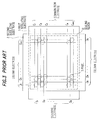
- Fig. 3 shows arrangement of electrodes of the plasma display panel.
- a plurality of the row and column electrodes cross each other in a right angle. Each crossing point forms a pixel 11.
- the row electrodes 3 are composed of two groups, one is that of scanning electrodes S 1 to S m and the other is that of common electrodes C 1 to C m+ 1 .
- the matrix region is sealed by a sealing region 12.
- Fig. 4 shows a timing chart of signals in a conventional method for driving a plasma display panel.
- the common electrodes C1 to C m+ 1 are supplied with maintaining pulses A periodically for maintaining discharge in the pixels 11, respectively.
- the scanning electrodes S 1 to S m are supplied with maintaining pulses B periodically in the same timing but different timing of the maintaining pulses A supplied to the common electrodes C 1 to C m+ 1 , respectively.
- Each of the scanning electrodes S 1 to S m is also supplied with a scanning pulse and an extinguishing pulse in different timings which comes in turn.
- the column electrodes D1 to D n are supplied with data pulses of positive in accordance with light emission data in the same timing as the scanning pulses supplied to the scanning electrodes S1 to S m .
- a data pulse of positive is supplied to the column electrode D1 synchronized with a scanning pulse supplied to the scanning electrode S 1. shown as (e) of Fig. 4. Accordingly, a discharge occurs in the pixel (S 1. D1) to make a light emission, shown as (f) of Fig. 4.
- This light emission is maintained by supplying the maintaining pulses A and B periodically to the scanning and column electrodes S 1 and D 1. however, the light emission terminates when an extinguishing pulse having a narrow width and a low voltage is supplied to the scanning electrode S 1. In the same manner, light emission operations of every pixels of the plasma display panel are carried out.
- Fig. 5 shows timing of light emission in the conventional method for driving a plasma display panel.
- One field for displaying one frame is divided to a plurality of sub-fields, and light emission time of each sub-field is controlled to display an image with gradation of brightness.
- the sub-fields have different light emission times of T, T/2, T/4, T/8, T/16 and T/32, respectively.
- the gradation of 64 grades can be realized by selecting one state from light emission and non-light emission in each sub-field.
- a method for driving a plasma display panel in a first preferred embodiment will be explained.
- the number of scanning electrodes is 480
- one field time is 1/60 sec.
- the sub-fields have different light emission times of T', T'/2, T'/4, T'/8, T'/16 and T'/32.
- a method for driving a plasma display panel in a second preferred embodiment will be explained.
- the sub-fields have different light emission times of T'', T''/2, T''/4, T''/8, T''/16 and T''/32, respectively.
- the scanning time during which all of the scanning electrodes are scanned becomes relatively short. If one field time is 1/60 sec., the scanning time which is approximately equal to T '' s becomes 1. 67 ms, compared with 2. 78 ms in the conventional method shown in Fig. 5. Therefore, the intervals of the scanning pulses as well as those of the maintaining pulses should be short. However, if the intervals of the maintaining pulses become short and the frequency thereof becomes high, the light emission efficiency may decrease, or power consumption having no contribution to light emission may increase, because currents for charging and discharging electrostatic capacity of the panel increase in proportion to the frequency of the maintaining pulses. Further, the pulse width of the scanning and maintaining pulses becomes narrow to cause instability of the discharge if the frequency of the maintaining pulses increases.
- Fig. 8 shows timing of signals in a method for driving a plasma display panel in a third preferred embodiment according to the invention.
- scanning electrodes S 1 to S m are divided to a plurality of groups.
- Bach group includes several scanning electrodes, though Fig. 8 shows a case of three electrodes.
- Each of the scanning electrodes S 1 to S 3 is supplied with a scanning pulse in turn at a different timing with the two others between the same interval of two maintaining pulses, then is supplied with an extinguishing pulse at the same timing with the two others.
- Each of the scanning electrodes S 4 to S 6 is also supplied with a scanning pulse and an extinguishing pulse, as shown in Fig. 8.
- the frequency of the maintaining pulses is sufficient to be one third of that in case of the conventional method.
- the pulse width of the maintaining and scanning pulses can be large. In Fig. 8, the pulse width of the maintaining pulses A and B is 1.5 micro seconds, and the pulse width of the scanning pulse is 2.5 micro seconds.
- Data pulses are supplied to a column electrode D j synchronized with each scanning pulse supplied to each scanning electrode.
- Table 1 shows frequencies of the pulses, the time using ratio, and the relative brightness in the conventional method and the methods in the first and second preferred embodiments, respectively.
- EXEMPLIFIED METHOD 1 represents the first preferred embodiment
- EXEMPLIFIED METHOD 2 represents combination of the first and third preferred embodiments in which the scanning electrodes are divided to pairs each of which is supplied with two scanning pulses in turn in the same interval between two maintaining pulses
- EXEMPLIFIED METHOD 3 represents combination of the second and third preferred embodiments in which the scanning electrodes are divided to pairs each of which is supplied with three scanning pulses in turn in the same interval between two maintaining pulses
- EXEMPLIFIED METHOD 4" represents combination of the second and third preferred embodiments in which the scanning electrodes are divided to pairs each of which is supplied with two scanning pulses in turn in the same interval between two maintaining pulses.
- the driving frequency becomes 1.17 times of that in the conventional method and the brightness becomes twice thereof in EXEMPLIFIED METHOD 1.
- EXEMPLIFIED METHOD 2 the brightness remains equal to that in the conventional method, however, the frequency of the maintaining pulses becomes half of that in the conventional method, so that the power consumption required for charging and discharging of electrostatic capacity of the panel becomes half thereof.
- EXEMPLIFIED METHOD 3 the frequency of the maintaining pulses becomes half of that in the conventional method, and moreover, the brightness is improved as compared with that in the conventional method.
- the frequency of the maintaining pulses becomes 0.8 times of that in the conventional method, and the brightness becomes twice thereof.
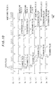
- the method can be used for driving a plasma display panel as shown in Figs. 1 to 3, however, the method can be also used for driving a plasma display panel of opposite electrode type in which row electrodes have only scanning electrodes as shown in Fig. 9.
- Fig. 10 shows timing of signals in the plasma display panel of opposite electrode type. The timings of the signals are the same as those in Fig. 8.
- This method may be adopted in a so called dividing driving method in which scanning electrodes are divided to two groups such that the scanning electrodes are alternately led out from opposed ends of the panel and column electrodes are divided to two groups such that all column electrodes are separated at central region of the panel so as to be led out from opposed ends of the panel, respectively.
- this method may be adopted in a so called interlace method in which one frame consists of two fields.
Landscapes
- Engineering & Computer Science (AREA)
- Physics & Mathematics (AREA)
- Computer Hardware Design (AREA)
- General Physics & Mathematics (AREA)
- Theoretical Computer Science (AREA)
- Plasma & Fusion (AREA)
- Power Engineering (AREA)
- Multimedia (AREA)
- Signal Processing (AREA)
- Control Of Indicators Other Than Cathode Ray Tubes (AREA)
- Control Of Gas Discharge Display Tubes (AREA)
- Transforming Electric Information Into Light Information (AREA)
Applications Claiming Priority (2)
| Application Number | Priority Date | Filing Date | Title |
|---|---|---|---|
| JP327066/90 | 1990-11-28 | ||
| JP2327066A JP2932686B2 (ja) | 1990-11-28 | 1990-11-28 | プラズマディスプレイパネルの駆動方法 |
Publications (3)
| Publication Number | Publication Date |
|---|---|
| EP0488326A2 true EP0488326A2 (fr) | 1992-06-03 |
| EP0488326A3 EP0488326A3 (en) | 1992-10-14 |
| EP0488326B1 EP0488326B1 (fr) | 1996-03-06 |
Family
ID=18194917
Family Applications (1)
| Application Number | Title | Priority Date | Filing Date |
|---|---|---|---|
| EP91120450A Expired - Lifetime EP0488326B1 (fr) | 1990-11-28 | 1991-11-28 | Méthode de commande pour un panneau d'affichage à plasma |
Country Status (4)
| Country | Link |
|---|---|
| US (1) | US5317334A (fr) |
| EP (1) | EP0488326B1 (fr) |
| JP (1) | JP2932686B2 (fr) |
| DE (1) | DE69117675T2 (fr) |
Cited By (23)
| Publication number | Priority date | Publication date | Assignee | Title |
|---|---|---|---|---|
| FR2709365A1 (fr) * | 1993-08-23 | 1995-03-03 | Samsung Display Devices Co Ltd | Procédé de pilotage d'un tableau d'affichage à plasma. |
| WO1996041326A1 (fr) * | 1995-06-07 | 1996-12-19 | Silicon Light Machines | Modulation de temps binaire a periodes mortes pour systemes d'affichage matriciels |
| FR2738655A1 (fr) * | 1995-09-12 | 1997-03-14 | Samsung Display Devices Co Ltd | Procede pour commander un dispositif d'affichage a plasma |
| WO1997040487A1 (fr) * | 1996-04-22 | 1997-10-30 | Silicon Light Machines, Inc. | Systeme d'affichage numerique a modulation d'impulsions en largeur et plan de memoire d'image a multiprogrammation autonome |
| EP0807919A1 (fr) * | 1996-05-13 | 1997-11-19 | Hitachi, Ltd. | Dispositif et procédé d'affichage |
| EP0834856A1 (fr) * | 1996-10-01 | 1998-04-08 | Lg Electronics Inc. | Méthode de commande d'un panneau d'affichage à plasma à courant alternatif |
| FR2755281A1 (fr) * | 1996-10-12 | 1998-04-30 | Soosan Heavy Ind Co Ltd | Dispositif et procede pour regler l'echelle des gris d'un systeme d'affichage moyennant l'utilisation d'un adressage irregulier |
| EP0890941A1 (fr) * | 1997-07-07 | 1999-01-13 | Matsushita Electric Industrial Co., Ltd. | Méthode pour l'affichage de niveaux de gris dans un panneau d'affichage à plasma |
| EP0899708A1 (fr) * | 1997-09-01 | 1999-03-03 | Samsung Display Devices Co., Ltd. | Dispositif d'affichage d'image par plasma et son procédé de commande |
| EP0964383A1 (fr) | 1998-06-11 | 1999-12-15 | Fujitsu Limited | Procédé et circuit de commande pour un panneau à plasma |
| US6064404A (en) * | 1996-11-05 | 2000-05-16 | Silicon Light Machines | Bandwidth and frame buffer size reduction in a digital pulse-width-modulated display system |
| EP1014331A1 (fr) * | 1998-12-08 | 2000-06-28 | Deutsche Thomson-Brandt Gmbh | Méthode de commande d'un panneau d'affichage à plasma |
| EP0938073A3 (fr) * | 1998-02-24 | 2000-08-02 | Lg Electronics Inc. | Circuit et dispositif de commande d'un panneau d'affichage à plasma |
| FR2791801A1 (fr) * | 1999-03-31 | 2000-10-06 | Nec Corp | Procede de commande et circuit de commande d'un panneau d4affichage a plasma |
| US6373451B1 (en) * | 1999-03-02 | 2002-04-16 | Samsung Sdi Co., Ltd. | Method for driving AC plasma display panel |
| US6492776B2 (en) | 2000-04-20 | 2002-12-10 | James C. Rutherford | Method for driving a plasma display panel |
| US6587084B1 (en) | 1998-07-10 | 2003-07-01 | Orion Electric Co., Ltd. | Driving method of a plasma display panel of alternating current for creation of gray level gradations |
| EP1197941A3 (fr) * | 2000-10-13 | 2003-12-10 | Samsung SDI Co. Ltd. | Méthode d'attaque d'un dispositif d'affichage à plasma |
| US6785001B2 (en) | 2001-08-21 | 2004-08-31 | Silicon Light Machines, Inc. | Method and apparatus for measuring wavelength jitter of light signal |
| US6839479B2 (en) | 2002-05-29 | 2005-01-04 | Silicon Light Machines Corporation | Optical switch |
| US7046420B1 (en) | 2003-02-28 | 2006-05-16 | Silicon Light Machines Corporation | MEM micro-structures and methods of making the same |
| EP1262945A3 (fr) * | 1995-08-03 | 2007-02-07 | Hitachi, Ltd. | Panneau d'affichage au plasma, procédé de commande pour le même et dispositif d'affichage au plasma avec impulsions d'entretien en opposition de phase pour lignes contigües |
| US9641826B1 (en) | 2011-10-06 | 2017-05-02 | Evans & Sutherland Computer Corporation | System and method for displaying distant 3-D stereo on a dome surface |
Families Citing this family (77)
| Publication number | Priority date | Publication date | Assignee | Title |
|---|---|---|---|---|
| US6535187B1 (en) * | 1998-04-21 | 2003-03-18 | Lawson A. Wood | Method for using a spatial light modulator |
| US6787995B1 (en) * | 1992-01-28 | 2004-09-07 | Fujitsu Limited | Full color surface discharge type plasma display device |
| US5731796A (en) * | 1992-10-15 | 1998-03-24 | Hitachi, Ltd. | Liquid crystal display driving method/driving circuit capable of being driven with equal voltages |
| WO1995013601A1 (fr) * | 1993-11-09 | 1995-05-18 | Honeywell Inc. | Appareil d'affichage cloisonne |
| US5943032A (en) * | 1993-11-17 | 1999-08-24 | Fujitsu Limited | Method and apparatus for controlling the gray scale of plasma display device |
| USRE40769E1 (en) * | 1993-11-17 | 2009-06-23 | Hitachi, Ltd. | Method and apparatus for controlling the gray scale of plasma display device |
| US6362835B1 (en) * | 1993-11-23 | 2002-03-26 | Texas Instruments Incorporated | Brightness and contrast control for a digital pulse-width modulated display system |
| US5684499A (en) * | 1993-11-29 | 1997-11-04 | Nec Corporation | Method of driving plasma display panel having improved operational margin |
| JP3309593B2 (ja) * | 1994-10-28 | 2002-07-29 | 松下電器産業株式会社 | プラズマディスプレイ |
| JP3499058B2 (ja) * | 1995-09-13 | 2004-02-23 | 富士通株式会社 | プラズマディスプレイの駆動方法及びプラズマディスプレイ装置 |
| CA2185592A1 (fr) | 1995-09-20 | 1997-03-21 | Masaji Ishigaki | Methode et dispositif d'affichage des teintes incorporees aux signaux de television |
| JP3322809B2 (ja) | 1995-10-24 | 2002-09-09 | 富士通株式会社 | ディスプレイ駆動方法及び装置 |
| JP3617206B2 (ja) * | 1996-08-16 | 2005-02-02 | セイコーエプソン株式会社 | 表示装置、電子機器及び駆動方法 |
| TW366512B (en) * | 1996-09-18 | 1999-08-11 | Matsushita Electric Industrial Co Ltd | Plasma display device and the brightness control method |
| JP3179036B2 (ja) * | 1996-10-14 | 2001-06-25 | 三菱電機株式会社 | ディスプレイ装置 |
| JP3672697B2 (ja) * | 1996-11-27 | 2005-07-20 | 富士通株式会社 | プラズマディスプレイ装置 |
| US6288693B1 (en) * | 1996-11-30 | 2001-09-11 | Lg Electronics Inc. | Plasma display panel driving method |
| TW371386B (en) | 1996-12-06 | 1999-10-01 | Matsushita Electric Industrial Co Ltd | Video display monitor using subfield method |
| US6215469B1 (en) | 1997-06-25 | 2001-04-10 | Matsushita Electric Industrial Co., Ltd. | Image display method |
| JP3596846B2 (ja) * | 1997-07-22 | 2004-12-02 | パイオニア株式会社 | プラズマディスプレイパネルの駆動方法 |
| US6872984B1 (en) | 1998-07-29 | 2005-03-29 | Silicon Light Machines Corporation | Method of sealing a hermetic lid to a semiconductor die at an angle |
| US6567059B1 (en) | 1998-11-20 | 2003-05-20 | Pioneer Corporation | Plasma display panel driving apparatus |
| TW516014B (en) * | 1999-01-22 | 2003-01-01 | Matsushita Electric Industrial Co Ltd | Driving method for AC plasma display panel |
| US6697084B1 (en) | 1999-03-04 | 2004-02-24 | Texas Instruments Incorporated | Tone display method |
| US6271811B1 (en) | 1999-03-12 | 2001-08-07 | Nec Corporation | Method of driving plasma display panel having improved operational margin |
| JP2000322025A (ja) * | 1999-05-14 | 2000-11-24 | Nec Corp | プラズマディスプレイ装置 |
| JP3613451B2 (ja) | 1999-07-27 | 2005-01-26 | パイオニア株式会社 | 多色発光表示パネルの駆動装置及び駆動方法 |
| JP3560143B2 (ja) * | 2000-02-28 | 2004-09-02 | 日本電気株式会社 | プラズマディスプレイパネルの駆動方法及び駆動回路 |
| US7177081B2 (en) | 2001-03-08 | 2007-02-13 | Silicon Light Machines Corporation | High contrast grating light valve type device |
| US6624588B2 (en) * | 2001-06-22 | 2003-09-23 | Pioneer Corporation | Method of driving plasma display panel |
| US6782205B2 (en) | 2001-06-25 | 2004-08-24 | Silicon Light Machines | Method and apparatus for dynamic equalization in wavelength division multiplexing |
| US6829092B2 (en) | 2001-08-15 | 2004-12-07 | Silicon Light Machines, Inc. | Blazed grating light valve |
| US6930364B2 (en) | 2001-09-13 | 2005-08-16 | Silicon Light Machines Corporation | Microelectronic mechanical system and methods |
| US6956995B1 (en) | 2001-11-09 | 2005-10-18 | Silicon Light Machines Corporation | Optical communication arrangement |
| US6800238B1 (en) | 2002-01-15 | 2004-10-05 | Silicon Light Machines, Inc. | Method for domain patterning in low coercive field ferroelectrics |
| US6767751B2 (en) | 2002-05-28 | 2004-07-27 | Silicon Light Machines, Inc. | Integrated driver process flow |
| US7054515B1 (en) | 2002-05-30 | 2006-05-30 | Silicon Light Machines Corporation | Diffractive light modulator-based dynamic equalizer with integrated spectral monitor |
| US6822797B1 (en) | 2002-05-31 | 2004-11-23 | Silicon Light Machines, Inc. | Light modulator structure for producing high-contrast operation using zero-order light |
| US6908201B2 (en) | 2002-06-28 | 2005-06-21 | Silicon Light Machines Corporation | Micro-support structures |
| US6813059B2 (en) | 2002-06-28 | 2004-11-02 | Silicon Light Machines, Inc. | Reduced formation of asperities in contact micro-structures |
| US6801354B1 (en) | 2002-08-20 | 2004-10-05 | Silicon Light Machines, Inc. | 2-D diffraction grating for substantially eliminating polarization dependent losses |
| US7057795B2 (en) | 2002-08-20 | 2006-06-06 | Silicon Light Machines Corporation | Micro-structures with individually addressable ribbon pairs |
| US6712480B1 (en) | 2002-09-27 | 2004-03-30 | Silicon Light Machines | Controlled curvature of stressed micro-structures |
| US6928207B1 (en) | 2002-12-12 | 2005-08-09 | Silicon Light Machines Corporation | Apparatus for selectively blocking WDM channels |
| US6987600B1 (en) | 2002-12-17 | 2006-01-17 | Silicon Light Machines Corporation | Arbitrary phase profile for better equalization in dynamic gain equalizer |
| US7057819B1 (en) | 2002-12-17 | 2006-06-06 | Silicon Light Machines Corporation | High contrast tilting ribbon blazed grating |
| US6934070B1 (en) | 2002-12-18 | 2005-08-23 | Silicon Light Machines Corporation | Chirped optical MEM device |
| US6927891B1 (en) | 2002-12-23 | 2005-08-09 | Silicon Light Machines Corporation | Tilt-able grating plane for improved crosstalk in 1×N blaze switches |
| US7068372B1 (en) | 2003-01-28 | 2006-06-27 | Silicon Light Machines Corporation | MEMS interferometer-based reconfigurable optical add-and-drop multiplexor |
| US7286764B1 (en) | 2003-02-03 | 2007-10-23 | Silicon Light Machines Corporation | Reconfigurable modulator-based optical add-and-drop multiplexer |
| US6947613B1 (en) | 2003-02-11 | 2005-09-20 | Silicon Light Machines Corporation | Wavelength selective switch and equalizer |
| US6922272B1 (en) | 2003-02-14 | 2005-07-26 | Silicon Light Machines Corporation | Method and apparatus for leveling thermal stress variations in multi-layer MEMS devices |
| US6806997B1 (en) | 2003-02-28 | 2004-10-19 | Silicon Light Machines, Inc. | Patterned diffractive light modulator ribbon for PDL reduction |
| US7391973B1 (en) | 2003-02-28 | 2008-06-24 | Silicon Light Machines Corporation | Two-stage gain equalizer |
| US6922273B1 (en) | 2003-02-28 | 2005-07-26 | Silicon Light Machines Corporation | PDL mitigation structure for diffractive MEMS and gratings |
| US7042611B1 (en) | 2003-03-03 | 2006-05-09 | Silicon Light Machines Corporation | Pre-deflected bias ribbons |
| US7639214B2 (en) | 2004-11-19 | 2009-12-29 | Lg Electronics Inc. | Plasma display apparatus and driving method thereof |
| EP1659558A3 (fr) * | 2004-11-19 | 2007-03-14 | LG Electronics, Inc. | Appareil d'affichage à plasma et méthode de commande pour la délivrance des implusions d'entretien |
| US7583241B2 (en) * | 2004-11-19 | 2009-09-01 | Lg Electronics Inc. | Plasma display apparatus and driving method of the same |
| CN101617354A (zh) | 2006-12-12 | 2009-12-30 | 埃文斯和萨瑟兰计算机公司 | 用于校准单个调制器投影仪中的rgb光的系统和方法 |
| US8358317B2 (en) | 2008-05-23 | 2013-01-22 | Evans & Sutherland Computer Corporation | System and method for displaying a planar image on a curved surface |
| US8702248B1 (en) | 2008-06-11 | 2014-04-22 | Evans & Sutherland Computer Corporation | Projection method for reducing interpixel gaps on a viewing surface |
| US8077378B1 (en) | 2008-11-12 | 2011-12-13 | Evans & Sutherland Computer Corporation | Calibration system and method for light modulation device |
| US9220132B2 (en) | 2013-06-22 | 2015-12-22 | Robert G. Marcotte | Breakover conduction illumination devices and operating method |
| JP2015115789A (ja) * | 2013-12-12 | 2015-06-22 | ソニー株式会社 | 撮像装置、撮像信号処理回路、及び、撮像信号処理方法、並びに、表示装置、画像信号処理回路、及び、画像信号処理方法 |
| US11030942B2 (en) | 2017-10-13 | 2021-06-08 | Jasper Display Corporation | Backplane adaptable to drive emissive pixel arrays of differing pitches |
| US10951875B2 (en) | 2018-07-03 | 2021-03-16 | Raxium, Inc. | Display processing circuitry |
| US11710445B2 (en) | 2019-01-24 | 2023-07-25 | Google Llc | Backplane configurations and operations |
| US11637219B2 (en) | 2019-04-12 | 2023-04-25 | Google Llc | Monolithic integration of different light emitting structures on a same substrate |
| US11238782B2 (en) | 2019-06-28 | 2022-02-01 | Jasper Display Corp. | Backplane for an array of emissive elements |
| US11626062B2 (en) | 2020-02-18 | 2023-04-11 | Google Llc | System and method for modulating an array of emissive elements |
| US12107072B2 (en) | 2020-04-06 | 2024-10-01 | Google Llc | Display backplane including an array of tiles |
| CN111445868B (zh) * | 2020-04-26 | 2021-11-02 | Tcl华星光电技术有限公司 | 背光单元及其控制方法、液晶显示装置 |
| US12573349B2 (en) | 2020-06-29 | 2026-03-10 | Google Llc | Efficient image data delivery for an array of pixel memory cells |
| US11538431B2 (en) | 2020-06-29 | 2022-12-27 | Google Llc | Larger backplane suitable for high speed applications |
| KR102890923B1 (ko) | 2020-12-21 | 2025-11-26 | 구글 엘엘씨 | 자동시청 3d 디스플레이용 고밀도 픽셀 어레이 |
| EP4371104A4 (fr) | 2021-07-14 | 2025-06-11 | Google LLC | Fond de panier et procédé de modulation de largeur d'impulsion |
Family Cites Families (5)
| Publication number | Priority date | Publication date | Assignee | Title |
|---|---|---|---|---|
| US4097780A (en) * | 1976-08-17 | 1978-06-27 | Bell Telephone Laboratories, Incorporated | Method and apparatus for energizing the cells of a plasma display panel to selected brightness levels |
| JP2751188B2 (ja) * | 1988-03-18 | 1998-05-18 | 富士通株式会社 | ガス放電表示パネルの駆動方法 |
| JPH02219092A (ja) * | 1989-02-20 | 1990-08-31 | Fujitsu General Ltd | 交流型プラズマディスプレイパネルの駆動方法 |
| JP2680429B2 (ja) * | 1989-06-16 | 1997-11-19 | 日本放送協会 | メモリ型表示パネルの中間調表示方式 |
| JP2720607B2 (ja) * | 1990-03-02 | 1998-03-04 | 株式会社日立製作所 | 表示装置、階調表示方法及び駆動回路 |
-
1990
- 1990-11-28 JP JP2327066A patent/JP2932686B2/ja not_active Expired - Fee Related
-
1991
- 1991-11-27 US US07/800,575 patent/US5317334A/en not_active Expired - Lifetime
- 1991-11-28 EP EP91120450A patent/EP0488326B1/fr not_active Expired - Lifetime
- 1991-11-28 DE DE69117675T patent/DE69117675T2/de not_active Expired - Fee Related
Cited By (34)
| Publication number | Priority date | Publication date | Assignee | Title |
|---|---|---|---|---|
| FR2709365A1 (fr) * | 1993-08-23 | 1995-03-03 | Samsung Display Devices Co Ltd | Procédé de pilotage d'un tableau d'affichage à plasma. |
| WO1996041326A1 (fr) * | 1995-06-07 | 1996-12-19 | Silicon Light Machines | Modulation de temps binaire a periodes mortes pour systemes d'affichage matriciels |
| US7705806B2 (en) | 1995-08-03 | 2010-04-27 | Hitachi Plasma Patent Licensing Co., Ltd | Method for driving a plasma display panel |
| EP1262945A3 (fr) * | 1995-08-03 | 2007-02-07 | Hitachi, Ltd. | Panneau d'affichage au plasma, procédé de commande pour le même et dispositif d'affichage au plasma avec impulsions d'entretien en opposition de phase pour lignes contigües |
| EP1262946A3 (fr) * | 1995-08-03 | 2007-06-20 | Hitachi Plasma Patent Licensing Co., Ltd. | Panneau d'affichage au plasma, procédé de commande pour le même et dispositif d'affichage au plasma avec décharges entre une électrode d'attaque et deux électrodes d'entretien contigües se produisant en séquence |
| FR2738655A1 (fr) * | 1995-09-12 | 1997-03-14 | Samsung Display Devices Co Ltd | Procede pour commander un dispositif d'affichage a plasma |
| US5936355A (en) * | 1995-09-12 | 1999-08-10 | Samsung Display Devices Co., Ltd. | Method for driving a plasma display to enhance brightness |
| WO1997040487A1 (fr) * | 1996-04-22 | 1997-10-30 | Silicon Light Machines, Inc. | Systeme d'affichage numerique a modulation d'impulsions en largeur et plan de memoire d'image a multiprogrammation autonome |
| EP0807919A1 (fr) * | 1996-05-13 | 1997-11-19 | Hitachi, Ltd. | Dispositif et procédé d'affichage |
| US6151000A (en) * | 1996-05-13 | 2000-11-21 | Hitachi, Ltd. | Display apparatus and display method thereof |
| EP0834856A1 (fr) * | 1996-10-01 | 1998-04-08 | Lg Electronics Inc. | Méthode de commande d'un panneau d'affichage à plasma à courant alternatif |
| FR2755281A1 (fr) * | 1996-10-12 | 1998-04-30 | Soosan Heavy Ind Co Ltd | Dispositif et procede pour regler l'echelle des gris d'un systeme d'affichage moyennant l'utilisation d'un adressage irregulier |
| US6064404A (en) * | 1996-11-05 | 2000-05-16 | Silicon Light Machines | Bandwidth and frame buffer size reduction in a digital pulse-width-modulated display system |
| EP0890941A1 (fr) * | 1997-07-07 | 1999-01-13 | Matsushita Electric Industrial Co., Ltd. | Méthode pour l'affichage de niveaux de gris dans un panneau d'affichage à plasma |
| US6236380B1 (en) | 1997-07-07 | 2001-05-22 | Matsushita Electric Industrial Co., Ltd. | Method for displaying gradation with plasma display panel |
| US6232935B1 (en) | 1997-09-01 | 2001-05-15 | Samsung Sdi Co., Ltd. | Plasma display panel and method for driving the same |
| EP0899708A1 (fr) * | 1997-09-01 | 1999-03-03 | Samsung Display Devices Co., Ltd. | Dispositif d'affichage d'image par plasma et son procédé de commande |
| CN100458896C (zh) * | 1997-09-01 | 2009-02-04 | 三星电管株式会社 | 等离子体显示板及其驱动方法 |
| EP0938073A3 (fr) * | 1998-02-24 | 2000-08-02 | Lg Electronics Inc. | Circuit et dispositif de commande d'un panneau d'affichage à plasma |
| US6256002B1 (en) | 1998-06-11 | 2001-07-03 | Fujitsu Limited | Method for driving a plasma display panel |
| EP0964383A1 (fr) | 1998-06-11 | 1999-12-15 | Fujitsu Limited | Procédé et circuit de commande pour un panneau à plasma |
| US6587084B1 (en) | 1998-07-10 | 2003-07-01 | Orion Electric Co., Ltd. | Driving method of a plasma display panel of alternating current for creation of gray level gradations |
| EP1014331A1 (fr) * | 1998-12-08 | 2000-06-28 | Deutsche Thomson-Brandt Gmbh | Méthode de commande d'un panneau d'affichage à plasma |
| US6373451B1 (en) * | 1999-03-02 | 2002-04-16 | Samsung Sdi Co., Ltd. | Method for driving AC plasma display panel |
| US6803888B1 (en) | 1999-03-31 | 2004-10-12 | Nec Corporation | Drive method and drive circuit for plasma display panel |
| FR2791801A1 (fr) * | 1999-03-31 | 2000-10-06 | Nec Corp | Procede de commande et circuit de commande d'un panneau d4affichage a plasma |
| US7319442B2 (en) | 1999-03-31 | 2008-01-15 | Pioneer Corporation | Drive method and drive circuit for plasma display panel |
| US6492776B2 (en) | 2000-04-20 | 2002-12-10 | James C. Rutherford | Method for driving a plasma display panel |
| EP1197941A3 (fr) * | 2000-10-13 | 2003-12-10 | Samsung SDI Co. Ltd. | Méthode d'attaque d'un dispositif d'affichage à plasma |
| US6785001B2 (en) | 2001-08-21 | 2004-08-31 | Silicon Light Machines, Inc. | Method and apparatus for measuring wavelength jitter of light signal |
| US6839479B2 (en) | 2002-05-29 | 2005-01-04 | Silicon Light Machines Corporation | Optical switch |
| US7046420B1 (en) | 2003-02-28 | 2006-05-16 | Silicon Light Machines Corporation | MEM micro-structures and methods of making the same |
| US9641826B1 (en) | 2011-10-06 | 2017-05-02 | Evans & Sutherland Computer Corporation | System and method for displaying distant 3-D stereo on a dome surface |
| US10110876B1 (en) | 2011-10-06 | 2018-10-23 | Evans & Sutherland Computer Corporation | System and method for displaying images in 3-D stereo |
Also Published As
| Publication number | Publication date |
|---|---|
| JP2932686B2 (ja) | 1999-08-09 |
| DE69117675T2 (de) | 1996-08-08 |
| EP0488326A3 (en) | 1992-10-14 |
| JPH04195087A (ja) | 1992-07-15 |
| US5317334A (en) | 1994-05-31 |
| EP0488326B1 (fr) | 1996-03-06 |
| DE69117675D1 (de) | 1996-04-11 |
Similar Documents
| Publication | Publication Date | Title |
|---|---|---|
| EP0488326B1 (fr) | Méthode de commande pour un panneau d'affichage à plasma | |
| US5107182A (en) | Plasma display and method of driving the same | |
| US6587084B1 (en) | Driving method of a plasma display panel of alternating current for creation of gray level gradations | |
| US6278420B1 (en) | Plasma display panel and driving method thereof | |
| US6903709B2 (en) | Plasma display panel and method of driving the same | |
| US6236380B1 (en) | Method for displaying gradation with plasma display panel | |
| US8094093B2 (en) | Plasma display apparatus | |
| US20020063701A1 (en) | Display device | |
| US6127992A (en) | Method of driving electric discharge panel | |
| US5789862A (en) | Surface discharge AC plasma display panel | |
| JP2674485B2 (ja) | 放電表示装置の駆動方法 | |
| JP3087840B2 (ja) | プラズマディスプレイの駆動方法 | |
| JP2000194319A (ja) | プラズマ・ディスプレイ、その画像表示方法 | |
| US7075243B2 (en) | Driving apparatus for plasma display panel and gray level expressing method thereof | |
| US7079090B2 (en) | Driving method for a plasma display panel and plasma display apparatus | |
| JP2907167B2 (ja) | カラープラズマディスプレイパネル | |
| KR20030044182A (ko) | 플라즈마 표시 패널의 구동방법 | |
| JPH1092323A (ja) | 表示パネル及びパネル型表示装置 | |
| US7123217B2 (en) | Method for driving plasma display panel | |
| US5155414A (en) | Driving method of plasma display panels | |
| JPH03219286A (ja) | プラズマディスプレイパネルの駆動方法 | |
| US6400342B2 (en) | Method of driving a plasma display panel before erase addressing | |
| US5162701A (en) | Plasma display and method of driving the same | |
| JP3390239B2 (ja) | プラズマディスプレイパネルの駆動方法 | |
| JP2003050561A (ja) | プラズマディスプレイパネルの駆動方法およびプラズマディスプレイパネル |
Legal Events
| Date | Code | Title | Description |
|---|---|---|---|
| PUAI | Public reference made under article 153(3) epc to a published international application that has entered the european phase |
Free format text: ORIGINAL CODE: 0009012 |
|
| 17P | Request for examination filed |
Effective date: 19911128 |
|
| AK | Designated contracting states |
Kind code of ref document: A2 Designated state(s): DE FR GB |
|
| PUAL | Search report despatched |
Free format text: ORIGINAL CODE: 0009013 |
|
| AK | Designated contracting states |
Kind code of ref document: A3 Designated state(s): DE FR GB |
|
| 17Q | First examination report despatched |
Effective date: 19940627 |
|
| GRAA | (expected) grant |
Free format text: ORIGINAL CODE: 0009210 |
|
| AK | Designated contracting states |
Kind code of ref document: B1 Designated state(s): DE FR GB |
|
| REF | Corresponds to: |
Ref document number: 69117675 Country of ref document: DE Date of ref document: 19960411 |
|
| ET | Fr: translation filed | ||
| PLBE | No opposition filed within time limit |
Free format text: ORIGINAL CODE: 0009261 |
|
| STAA | Information on the status of an ep patent application or granted ep patent |
Free format text: STATUS: NO OPPOSITION FILED WITHIN TIME LIMIT |
|
| 26N | No opposition filed | ||
| REG | Reference to a national code |
Ref country code: GB Ref legal event code: IF02 |
|
| REG | Reference to a national code |
Ref country code: GB Ref legal event code: 732E |
|
| REG | Reference to a national code |
Ref country code: FR Ref legal event code: TP |
|
| REG | Reference to a national code |
Ref country code: FR Ref legal event code: CD |
|
| REG | Reference to a national code |
Ref country code: GB Ref legal event code: 732E |
|
| REG | Reference to a national code |
Ref country code: FR Ref legal event code: TP |
|
| PGFP | Annual fee paid to national office [announced via postgrant information from national office to epo] |
Ref country code: DE Payment date: 20071122 Year of fee payment: 17 |
|
| PGFP | Annual fee paid to national office [announced via postgrant information from national office to epo] |
Ref country code: GB Payment date: 20071128 Year of fee payment: 17 Ref country code: FR Payment date: 20071108 Year of fee payment: 17 |
|
| GBPC | Gb: european patent ceased through non-payment of renewal fee |
Effective date: 20081128 |
|
| REG | Reference to a national code |
Ref country code: FR Ref legal event code: ST Effective date: 20090731 |
|
| PG25 | Lapsed in a contracting state [announced via postgrant information from national office to epo] |
Ref country code: DE Free format text: LAPSE BECAUSE OF NON-PAYMENT OF DUE FEES Effective date: 20090603 |
|
| PG25 | Lapsed in a contracting state [announced via postgrant information from national office to epo] |
Ref country code: GB Free format text: LAPSE BECAUSE OF NON-PAYMENT OF DUE FEES Effective date: 20081128 |
|
| PG25 | Lapsed in a contracting state [announced via postgrant information from national office to epo] |
Ref country code: FR Free format text: LAPSE BECAUSE OF NON-PAYMENT OF DUE FEES Effective date: 20081130 |