EP0488344A2 - Fabrication d'un corps du type SOI utilisant une croissance épitaxiale sélective - Google Patents
Fabrication d'un corps du type SOI utilisant une croissance épitaxiale sélective Download PDFInfo
- Publication number
- EP0488344A2 EP0488344A2 EP91120472A EP91120472A EP0488344A2 EP 0488344 A2 EP0488344 A2 EP 0488344A2 EP 91120472 A EP91120472 A EP 91120472A EP 91120472 A EP91120472 A EP 91120472A EP 0488344 A2 EP0488344 A2 EP 0488344A2
- Authority
- EP
- European Patent Office
- Prior art keywords
- semiconductor
- insulator
- substrate
- oxide
- semiconductor material
- Prior art date
- Legal status (The legal status is an assumption and is not a legal conclusion. Google has not performed a legal analysis and makes no representation as to the accuracy of the status listed.)
- Withdrawn
Links
Images


Classifications
-
- H—ELECTRICITY
- H10—SEMICONDUCTOR DEVICES; ELECTRIC SOLID-STATE DEVICES NOT OTHERWISE PROVIDED FOR
- H10P—GENERIC PROCESSES OR APPARATUS FOR THE MANUFACTURE OR TREATMENT OF DEVICES COVERED BY CLASS H10
- H10P90/00—Preparation of wafers not covered by a single main group of this subclass, e.g. wafer reinforcement
- H10P90/19—Preparing inhomogeneous wafers
- H10P90/1904—Preparing vertically inhomogeneous wafers
- H10P90/1906—Preparing SOI wafers
- H10P90/1912—Preparing SOI wafers using selective deposition, e.g. epitaxial lateral overgrowth [ELO] or selective deposition of single crystal silicon
-
- H—ELECTRICITY
- H10—SEMICONDUCTOR DEVICES; ELECTRIC SOLID-STATE DEVICES NOT OTHERWISE PROVIDED FOR
- H10W—GENERIC PACKAGES, INTERCONNECTIONS, CONNECTORS OR OTHER CONSTRUCTIONAL DETAILS OF DEVICES COVERED BY CLASS H10
- H10W10/00—Isolation regions in semiconductor bodies between components of integrated devices
- H10W10/01—Manufacture or treatment
- H10W10/011—Manufacture or treatment of isolation regions comprising dielectric materials
- H10W10/019—Manufacture or treatment of isolation regions comprising dielectric materials using epitaxial passivated integrated circuit [EPIC] processes
-
- H—ELECTRICITY
- H10—SEMICONDUCTOR DEVICES; ELECTRIC SOLID-STATE DEVICES NOT OTHERWISE PROVIDED FOR
- H10W—GENERIC PACKAGES, INTERCONNECTIONS, CONNECTORS OR OTHER CONSTRUCTIONAL DETAILS OF DEVICES COVERED BY CLASS H10
- H10W10/00—Isolation regions in semiconductor bodies between components of integrated devices
- H10W10/10—Isolation regions comprising dielectric materials
- H10W10/181—Semiconductor-on-insulator [SOI] isolation regions, e.g. buried oxide regions of SOI wafers
Definitions
- This invention generally relates to semiconductor fabrication methods and devices, and more specifically to semiconductor on insulator (SOI) fabrication methods and devices.
- SOI semiconductor on insulator
- SOI technologies have been investigated extensively for a number of applications including radiation resistant or radhard devices, high-performance high-speed IC's, and 3-D integrated devices.
- Various techniques have been investigated for SOI material formation. These include:
- SOS SIMOX
- SOI by wafer bonding are the most manufacturable techniques at present.
- SIMOX approach requires high-dose, high-energy O+ ion implantation.
- the optimization of the SIMOX material quality requires special attention to the implantation and subsequent annealing conditions.
- the single crystal silicon layer formed on the SIMOX wafer is rather thin (e.g. less than a few thousand ⁇ ).
- the wafer bonding techniques employ various bonding methods such as annealing, mechanical pressing and annealing, or electric-field pressing and annealing.
- Various interlayer insulators such as thermal silicon dioxide and doped oxide have been used.
- Typical wafer bonding processes are based on the Van der Walls forces which require extremely flat and defect free surfaces.
- the SOI material fabrication by ELO-SEG epipitaxial lateral overgrowth-selective epitaxial growth
- ELO-SEG epilasphide epitaxial growth
- the original oxide layer is patterned in order to provide silicon seed holes for SEG and subsequent lateral overgrowth.
- the method comprises: anisotropically etching a substrate to form trenches having walls and bottoms; anisotropically depositing oxide over a surface of the substrate and on the trench walls and bottoms; selective etching to remove trench wall oxide, but leaving oxide over the semiconductor surface and on the trench bottom, thereby creating sidewall seed holes which expose portions of the semiconductor substrate; epitaxially growing semiconductor material on the exposed portions of the semiconductor substrate to partially fill the trenches; depositing nitride; anisotropically etching the nitride to form nitride sidewalls; growing (e.g.
- thermally forming) oxide on top of the grown semiconductor material selectively removing nitride sidewalls; anisotropically etching exposed semiconductor until the buried oxide is reached, thereby leaving islands of selectively grown semiconductor material on the buried oxide layer; thermally growing oxide on areas of exposed semiconductor; anisotropically etching oxide to expose the top of the semiconductor islands; and epitaxially growing semiconductor material to merge the semiconductor islands and create a layer of single-crystal semiconductor material which is electrically insulated from the substrate.
- the method comprises: anisotropically etching a surface of the substrate to form trenches having sidewalls and bottoms; anisotropically depositing a first insulator over the substrate surface and on the trench walls and bottoms; etching to remove first insulator from the trench walls, but leaving first insulator over the semiconductor substrate surface and on the trench bottoms, thereby creating seed holes which expose portions of the semiconductor substrate; epitaxially growing semiconductor material on the exposed portions of the semiconductor substrate to partially fill the trenches; depositing sidewall forming material, the sidewall forming material being different from the first insulator; anisotropically etching the sidewall forming material to form sidewalls and to bare surfaces of the epitaxially grown semiconductor material; forming an etch mask material on the bare semiconductor material; removing the sidewalls and uncovering areas of semiconductor material; anisotropically etching the uncovered areas of semiconductor material until the first insulator on the trench bottoms is reached, thereby leaving islands of semiconductor material on the first insulator
- the first insulator and the second insulator are of the same material (most preferably oxide), the sidewall forming material is nitride, the growable etch mask is oxide, and the semiconductor is silicon.
- the wafer comprises: trenches having walls and bottoms in a single-crystal semiconductor (e.g. silicon) substrate; a first insulator (e.g. oxide) on a surface of the substrate and on the trench bottoms; a second insulator (e.g. oxide) on the trench walls; and a layer of single-crystal semiconductor material (e.g. silicon) on the surface and extending into the trenches, with the layer being electrically insulated from the substrate.
- a single-crystal semiconductor e.g. silicon
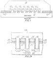
- FIG. 1 shows an example of a prior art semiconductor-on-insulator (SOI) wafer formed by a selective epitaxial growth - epitaxial lateral overgrowth (SEG-ELO) process.
- SOI semiconductor-on-insulator
- SEG-ELO selective epitaxial growth - epitaxial lateral overgrowth
- the number of seed holes 14 should be sufficiently large in order to allow for merging of the adjacent epitaxial islands, grown in the seed holes 14, in a reasonable epi process time without any defect formation at the merged interfaces.
- This condition makes the seed-to-seed spacing less than a few micrometers.
- the seed regions 14 provide an electrical link between the etched back epi layer 16 and silicon substrate 12, resulting in a degradation of epi-to-substrate electrical isolation.
- the number of seed holes 14 can be reduced, but this will increase the epi growth time in order to allow proper merging of the adjacent islands in the seed holes 14. Moreover, a longer etch back will be required to thin the epi layer 16 to the desired thickness.
- FIG. 2k A preferred embodiment of the present invention is shown in FIG. 2k.
- a method of making this preferred embodiment SOI wafer using an SEG-ELO process will be described with reference to FIGS. 2a-2k.
- a layer of masking material such as silicon dioxide (oxide) 20, approximately 5000 ⁇ thick, is formed on a silicon substrate 22 then patterned to achieve the structure shown in FIG. 2a.
- Trenches 24, approximately 2 um high and 1 um wide, are formed, as shown in FIG. 2b, using an anisotropic etch process, such as reactive ion etching (RIE).
- RIE reactive ion etching
- the trenches 24 may be formed with any appropriate masking step.
- a photoresist masking process may be used in conjunction with or in place of the oxide 20.
- a short thermal oxidation and wet etch may be performed to remove any residual surface damage from the etching process.
- the structure in FIG 2c is obtained by performing an anisotropic oxide deposition 26,28,34, approximately 1 um thick, using a plasma deposition technique such as electron cyclotron resonance (ECR) or magnetron plasma chemical vapor deposition.
- ECR electron cyclotron resonance
- a selective etch is performed to remove the sidewall oxide 28, exposing substrate sidewalls 30 in the trenches, therefore, creating sidewall seed holes for future SEG-ELO processes, as shown in FIG. 2d. Due to the different characteristics of the anisotropically deposited sidewall oxide 28 compared to the oxide films deposited on flat surfaces 26,34, it is possible to selectively strip the sidewall oxide 28 without removing a significant amount of oxide on the top and bottom surfaces 26,34.
- FIG. 2e shows the results of the first SEG process after the trenches are laterally filled preferably to the top of the silicon sidewalls 30, resulting in buried layers of oxide 34 within the silicon substrate 22.
- the resulting silicon surface 32 may have a small facet angle, resulting in an almost planar surface.
- An optional oxidation and etch may be done to remove defects before continuing with the next step.
- LPCVD low-pressure chemical vapor deposition
- anisotropic etching process such as RIE
- an optional oxidation and etch may be performed to remove any surface damage to exposed silicon 32.
- An optional second SEG process 38 may be performed vertically to completely fill the trenches, as shown in FIG. 2g.
- Oxide 40 is formed, approximately 500 ⁇ thick, on top of the exposed silicon 38.
- the nitride 36 is then selectively stripped using an etchant such as hot phosphoric acid or microwave plasma.
- An etchant such as hot phosphoric acid or microwave plasma.
- An anisotropic etch process such as RIE, is performed on the exposed silicon 42 until the buried oxide 34 is reached, leaving islands of silicon 44 on the buried oxide layers 34, as shown in FIG. 2i.
- An optional oxidation and etch may be done to remove any surface damage.
- the areas to the sides of the silicon islands 44 are filled with oxide 46 by first performing a short thermal oxidation followed by a conformal oxide deposition (e.g. TEOS).
- a conformal oxide deposition e.g. TEOS
- the oxide 40 is etched back to expose the top of the silicon islands 44, achieving the structure shown in FIG. 2j.
- an SEG-ELO process is done to merge the individual silicon islands 44.
- the epi layer 48 may then be etched back if a thinner layer is desired.
- the resultant structure is a fully isolated SOI based on SEG-ELO, as shown in FIG. 2k.
- the number of seed holes may be determined by the number needed to reduce fabrication cost, to improve material quality, and reduce the need for large epi thinning, without degrading the epi-to-substrate isolation.
- the suggested process seals all the seed holes with insulators resulting in an epitaxial layer on top of wafer which is completely insulated from the substrate. As a result, the usual trade-off between epi substrate isolation and fabrication cost/material quality is eliminated.
- the process flow is simple and uses only one mask to define the seed holes. No additional masking step is required. The sealing of the seed holes takes place using a self-aligned process.
- the substrate used is referred to as silicon, it could be any appropriate semiconductor material, such as GaAs or Ge.
- the oxide can be any insulator, and the nitride can be any material, other than the semiconductor and insulator previously used, that can be deposited and etched to achieve the desired results.
- an alternative embodiment may be used which reduces the number of epitaxial growth steps from three to two.
- the alternative emodiment is similar to the preferred embodiment up to FIG 2f.
- a thermal oxidation and subsequent selective istropic nitride etch are performed.
- a subsequent an isotropic etch froms the silicon islands 44 on the buried oxide layers 34.
- the structure is similar to FIG 2i, with the exception of the height of the silicon islands 44.
- the silicon islands 44 are shorter and recessed with respect to the top of the oxide 26 because the second SEG process was not done.
- the process continues by filling the areas to the sides of the silicon islands 44 with oxide 46 followed by a final SEG process to fill the remainder of the trenches and merge the silicon islands 44 to form an insulated epi layer 48.
- Wafers in accordance with the present invention or wafers made in accordance with the method of the present invention may be packaged into finished semi-conductor devices.
Landscapes
- Element Separation (AREA)
Applications Claiming Priority (4)
| Application Number | Priority Date | Filing Date | Title |
|---|---|---|---|
| US633647 | 1984-07-23 | ||
| US619785 | 1990-11-29 | ||
| US07/619,785 US5143862A (en) | 1990-11-29 | 1990-11-29 | SOI wafer fabrication by selective epitaxial growth |
| US07/633,647 US5102821A (en) | 1990-12-20 | 1990-12-20 | SOI/semiconductor heterostructure fabrication by wafer bonding of polysilicon to titanium |
Publications (2)
| Publication Number | Publication Date |
|---|---|
| EP0488344A2 true EP0488344A2 (fr) | 1992-06-03 |
| EP0488344A3 EP0488344A3 (en) | 1994-09-21 |
Family
ID=27088585
Family Applications (1)
| Application Number | Title | Priority Date | Filing Date |
|---|---|---|---|
| EP19910120472 Withdrawn EP0488344A3 (en) | 1990-11-29 | 1991-11-29 | Soi wafer fabrication by selective epitaxial growth |
Country Status (2)
| Country | Link |
|---|---|
| EP (1) | EP0488344A3 (fr) |
| JP (1) | JPH0697400A (fr) |
Cited By (8)
| Publication number | Priority date | Publication date | Assignee | Title |
|---|---|---|---|---|
| EP0763255A4 (fr) * | 1994-06-01 | 1999-03-17 | Litton Systems Inc | Element d'ancrage de substrat pour silicium depouille sur des microstructures d'isolateur |
| EP0929095A1 (fr) * | 1998-01-13 | 1999-07-14 | STMicroelectronics S.r.l. | Procédé pour fabriquer un substrat du type SOI |
| EP1049155A1 (fr) * | 1999-04-29 | 2000-11-02 | STMicroelectronics S.r.l. | Procédé de fabrication d'une pastille SOI avec des régions d'oxyde enterrées sans bout pointu |
| US6277703B1 (en) | 1998-05-15 | 2001-08-21 | Stmicroelectronics S.R.L. | Method for manufacturing an SOI wafer |
| US6559035B2 (en) | 1998-01-13 | 2003-05-06 | Stmicroelectronics S.R.L. | Method for manufacturing an SOI wafer |
| US6759746B1 (en) | 2000-03-17 | 2004-07-06 | Robert Bruce Davies | Die attachment and method |
| USRE41581E1 (en) | 1999-07-12 | 2010-08-24 | Robert Bruce Davies | Monolithic low dielectric constant platform for passive components and method |
| CN113937054A (zh) * | 2020-06-29 | 2022-01-14 | 长鑫存储技术有限公司 | 半导体结构及其制作方法 |
Families Citing this family (2)
| Publication number | Priority date | Publication date | Assignee | Title |
|---|---|---|---|---|
| JP5081394B2 (ja) * | 2006-05-19 | 2012-11-28 | ルネサスエレクトロニクス株式会社 | 半導体装置の製造方法 |
| US10153190B2 (en) * | 2014-02-05 | 2018-12-11 | Micron Technology, Inc. | Devices, systems and methods for electrostatic force enhanced semiconductor bonding |
Family Cites Families (4)
| Publication number | Priority date | Publication date | Assignee | Title |
|---|---|---|---|---|
| US4507158A (en) * | 1983-08-12 | 1985-03-26 | Hewlett-Packard Co. | Trench isolated transistors in semiconductor films |
| US4760036A (en) * | 1987-06-15 | 1988-07-26 | Delco Electronics Corporation | Process for growing silicon-on-insulator wafers using lateral epitaxial growth with seed window oxidation |
| US4758531A (en) * | 1987-10-23 | 1988-07-19 | International Business Machines Corporation | Method of making defect free silicon islands using SEG |
| EP0366013A3 (fr) * | 1988-10-27 | 1990-06-27 | Texas Instruments Incorporated | Déposition sélective d'un diélectrique sur des structures horizontales d'une partie d'un circuit intégré |
-
1991
- 1991-11-28 JP JP3314476A patent/JPH0697400A/ja active Pending
- 1991-11-29 EP EP19910120472 patent/EP0488344A3/en not_active Withdrawn
Cited By (9)
| Publication number | Priority date | Publication date | Assignee | Title |
|---|---|---|---|---|
| EP0763255A4 (fr) * | 1994-06-01 | 1999-03-17 | Litton Systems Inc | Element d'ancrage de substrat pour silicium depouille sur des microstructures d'isolateur |
| EP0929095A1 (fr) * | 1998-01-13 | 1999-07-14 | STMicroelectronics S.r.l. | Procédé pour fabriquer un substrat du type SOI |
| US6559035B2 (en) | 1998-01-13 | 2003-05-06 | Stmicroelectronics S.R.L. | Method for manufacturing an SOI wafer |
| US6277703B1 (en) | 1998-05-15 | 2001-08-21 | Stmicroelectronics S.R.L. | Method for manufacturing an SOI wafer |
| EP1049155A1 (fr) * | 1999-04-29 | 2000-11-02 | STMicroelectronics S.r.l. | Procédé de fabrication d'une pastille SOI avec des régions d'oxyde enterrées sans bout pointu |
| US6362070B1 (en) | 1999-04-29 | 2002-03-26 | Stmicroelectronics S.R.L. | Process for manufacturing a SOI wafer with buried oxide regions without cusps |
| USRE41581E1 (en) | 1999-07-12 | 2010-08-24 | Robert Bruce Davies | Monolithic low dielectric constant platform for passive components and method |
| US6759746B1 (en) | 2000-03-17 | 2004-07-06 | Robert Bruce Davies | Die attachment and method |
| CN113937054A (zh) * | 2020-06-29 | 2022-01-14 | 长鑫存储技术有限公司 | 半导体结构及其制作方法 |
Also Published As
| Publication number | Publication date |
|---|---|
| JPH0697400A (ja) | 1994-04-08 |
| EP0488344A3 (en) | 1994-09-21 |
Similar Documents
| Publication | Publication Date | Title |
|---|---|---|
| US5321298A (en) | Soi wafer fabrication by selective epitaxial growth | |
| US4948456A (en) | Confined lateral selective epitaxial growth | |
| US6319333B1 (en) | Silicon-on-insulator islands | |
| US4507158A (en) | Trench isolated transistors in semiconductor films | |
| US4509249A (en) | Method for fabricating isolation region in semiconductor devices | |
| EP0570043B1 (fr) | Puce SOI pour BICMOS comportant des régions SOI en silicium épaisses et minces | |
| US7947566B2 (en) | Method and apparatus for making coplanar isolated regions of different semiconductor materials on a substrate | |
| US6747333B1 (en) | Method and apparatus for STI using passivation material for trench bottom liner | |
| US4929566A (en) | Method of making dielectrically isolated integrated circuits using oxygen implantation and expitaxial growth | |
| GB2156149A (en) | Dielectrically-isolated integrated circuit manufacture | |
| US4891092A (en) | Method for making a silicon-on-insulator substrate | |
| US5882981A (en) | Mesa isolation Refill Process for Silicon on Insulator Technology Using Flowage Oxides as the Refill Material | |
| US6521510B1 (en) | Method for shallow trench isolation with removal of strained island edges | |
| US5185286A (en) | Process for producing laminated semiconductor substrate | |
| EP0488344A2 (fr) | Fabrication d'un corps du type SOI utilisant une croissance épitaxiale sélective | |
| US6534379B1 (en) | Linerless shallow trench isolation method | |
| US4704186A (en) | Recessed oxide method for making a silicon-on-insulator substrate | |
| KR100353174B1 (ko) | 절연체 상 실리콘 기판 제조 방법 | |
| US5909626A (en) | SOI substrate and fabrication process therefor | |
| KR100428526B1 (ko) | 절연체상실리콘기술을위한분리산화물을형성하는방법 | |
| US5686343A (en) | Process for isolating a semiconductor layer on an insulator | |
| JP3153632B2 (ja) | Soi構造の製造方法 | |
| KR20000073114A (ko) | 선택적 에피택셜 성장을 이용한 트렌치 소자 분리 방법 | |
| KR100456705B1 (ko) | 반도체 장치의 제조 공정 | |
| US7060596B2 (en) | Process for fabricating a single-crystal substrate and integrated circuit comprising such a substrate |
Legal Events
| Date | Code | Title | Description |
|---|---|---|---|
| PUAI | Public reference made under article 153(3) epc to a published international application that has entered the european phase |
Free format text: ORIGINAL CODE: 0009012 |
|
| AK | Designated contracting states |
Kind code of ref document: A2 Designated state(s): DE FR GB IT NL |
|
| PUAL | Search report despatched |
Free format text: ORIGINAL CODE: 0009013 |
|
| AK | Designated contracting states |
Kind code of ref document: A3 Designated state(s): DE FR GB IT NL |
|
| 17P | Request for examination filed |
Effective date: 19950302 |
|
| 17Q | First examination report despatched |
Effective date: 19950327 |
|
| STAA | Information on the status of an ep patent application or granted ep patent |
Free format text: STATUS: THE APPLICATION IS DEEMED TO BE WITHDRAWN |
|
| 18D | Application deemed to be withdrawn |
Effective date: 19980714 |