EP0489276B1 - Dispositif de modulation pour un amplificateur de puissance haute fréquence - Google Patents
Dispositif de modulation pour un amplificateur de puissance haute fréquence Download PDFInfo
- Publication number
- EP0489276B1 EP0489276B1 EP91119268A EP91119268A EP0489276B1 EP 0489276 B1 EP0489276 B1 EP 0489276B1 EP 91119268 A EP91119268 A EP 91119268A EP 91119268 A EP91119268 A EP 91119268A EP 0489276 B1 EP0489276 B1 EP 0489276B1
- Authority
- EP
- European Patent Office
- Prior art keywords
- pulse
- modulation
- control
- amplifier
- modulation device
- Prior art date
- Legal status (The legal status is an assumption and is not a legal conclusion. Google has not performed a legal analysis and makes no representation as to the accuracy of the status listed.)
- Expired - Lifetime
Links
- 230000010354 integration Effects 0.000 claims description 4
- 230000003111 delayed effect Effects 0.000 claims description 3
- 230000005540 biological transmission Effects 0.000 description 10
- 238000000034 method Methods 0.000 description 8
- 238000012937 correction Methods 0.000 description 7
- 230000000694 effects Effects 0.000 description 5
- 230000003321 amplification Effects 0.000 description 3
- 238000011156 evaluation Methods 0.000 description 3
- 238000003199 nucleic acid amplification method Methods 0.000 description 3
- 101100536250 Homo sapiens TMEM120A gene Proteins 0.000 description 2
- 102100028548 Ion channel TACAN Human genes 0.000 description 2
- 230000003679 aging effect Effects 0.000 description 2
- 238000011161 development Methods 0.000 description 2
- 230000018109 developmental process Effects 0.000 description 2
- 238000010586 diagram Methods 0.000 description 2
- 230000001105 regulatory effect Effects 0.000 description 2
- 238000007493 shaping process Methods 0.000 description 2
- 230000015572 biosynthetic process Effects 0.000 description 1
- 239000000872 buffer Substances 0.000 description 1
- 239000003990 capacitor Substances 0.000 description 1
- 230000015556 catabolic process Effects 0.000 description 1
- 238000004891 communication Methods 0.000 description 1
- 230000001276 controlling effect Effects 0.000 description 1
- 238000006731 degradation reaction Methods 0.000 description 1
- 230000001419 dependent effect Effects 0.000 description 1
- 238000005516 engineering process Methods 0.000 description 1
- 238000005259 measurement Methods 0.000 description 1
- 238000001208 nuclear magnetic resonance pulse sequence Methods 0.000 description 1
- 230000010355 oscillation Effects 0.000 description 1
- 238000012887 quadratic function Methods 0.000 description 1
- 230000000630 rising effect Effects 0.000 description 1
- 238000004904 shortening Methods 0.000 description 1
- 239000007787 solid Substances 0.000 description 1
Images

Classifications
-
- H—ELECTRICITY
- H03—ELECTRONIC CIRCUITRY
- H03G—CONTROL OF AMPLIFICATION
- H03G3/00—Gain control in amplifiers or frequency changers
- H03G3/20—Automatic control
- H03G3/30—Automatic control in amplifiers having semiconductor devices
- H03G3/3036—Automatic control in amplifiers having semiconductor devices in high-frequency amplifiers or in frequency-changers
- H03G3/3042—Automatic control in amplifiers having semiconductor devices in high-frequency amplifiers or in frequency-changers in modulators, frequency-changers, transmitters or power amplifiers
- H03G3/3047—Automatic control in amplifiers having semiconductor devices in high-frequency amplifiers or in frequency-changers in modulators, frequency-changers, transmitters or power amplifiers for intermittent signals, e.g. burst signals
-
- H—ELECTRICITY
- H03—ELECTRONIC CIRCUITRY
- H03C—MODULATION
- H03C5/00—Amplitude modulation and angle modulation produced simultaneously or at will by the same modulating signal
-
- H—ELECTRICITY
- H03—ELECTRONIC CIRCUITRY
- H03F—AMPLIFIERS
- H03F1/00—Details of amplifiers with only discharge tubes, only semiconductor devices or only unspecified devices as amplifying elements
- H03F1/32—Modifications of amplifiers to reduce non-linear distortion
- H03F1/3241—Modifications of amplifiers to reduce non-linear distortion using predistortion circuits
Definitions
- the invention relates to a modulation device according to the preamble of claim 1.
- the invention is based on pulse power amplifiers using RF power transistors, while pulse amplification is to be carried out at the same time according to a predetermined envelope curve during the amplification of RF pulses to a high output power and the pulse peak power is to assume a desired value.
- the generation of transmit pulses with a defined envelope basically represents an amplitude modulation.
- DE-C-28 35 751 mentions that the known teaching for regulating the modulation signal is not readily based on RF power amplifiers in which the RF carrier oscillation modulates with pulses will be transferable. This applies in particular if the pulses only have a short pulse duration, e.g. 8 »sec, have. The time required for the known regulation is too long for these applications.
- an RF power amplifier is known in detail, in which the correction is carried out in the transmission pauses by using buffers.
- the control loop is interrupted during the correction.
- the transmission mode is switched from the "transmission” mode to the "correction” mode. It is assumed that the transmission signal has relatively long pauses between the transmission pulses or the pulse groups, as is the case with the distance measuring system DME or the navigation system TACAN.
- the RF power amplifier exists the pulse sequence of 100 or more pulses per message, it being possible to switch between two pulses to a different carrier frequency and from a first to a second pulse format. In these cases, with the aid of the amplifier described, it is not possible, for reasons of time, to predistort the modulation signal in a suitable manner, since for correction all setpoint and actual amplitude values of all pulses of a pulse group would have to be compared with one another.
- a high-frequency pulse amplifier in which an amplifier chain is regulated to a constant output power by means of an AGC control loop.
- a constant current source is assigned to each of the transistor amplifier stages.
- the control pulses for all constant current sources run via a common pulse shaper circuit and are adjusted with regard to their voltage amplitude, specifically by an AGC control voltage which is obtained as a function of the total actual output power of the amplifier stages in comparison with the target output power to be kept constant.
- the edges of the pulses emitted by the pulse shaping circuit, which control the constant current sources, align the edges of the high-frequency pulses passing through the amplifier stages and can be formed as required.
- the AGC control loop provided here regulates the output power of the amplifier stages as a function of the change in amplitude of the envelope.
- the time constant in an AGC circuit is always chosen to be so large that an average DC voltage is formed from the successive high-frequency pulses, the value of which is therefore proportional to the amplitude of the RF pulses. This problem is dealt with in DE-C-12 97 703.
- the envelope of the high-frequency pulses can be obtained from the amplifier output signal by appropriate selection of the time constant of the rectifier circuit.
- a transistor power amplifier for DME applications is known from the article by D. Graziani: “Solid State Amplifiers for DME Beacons” in the magazine “Electrical Communication", Vol. 50, No. 4, 1975, pages 273 to 277, in which the modulation control pulse has a "socket".
- the reason for this modulation technique lies in the initial non-linearity of the control characteristic between the output power and the modulation pulse amplitude.
- the non-linearity at low modulation voltage causes a change in the pulse shape by shortening the rise and fall times.
- the modulation technique specified here by means of predistortion of the modulation control pulse has the disadvantage of being a pure control process.
- Pulse power amplifiers that generate peak pulse powers of 200 W and more up to the GHz range use RF power transistors for pulse operation.
- the transistors work in non-linear C mode and are only controlled during keying in A and B mode (DE-C-29 04 011).
- a non-linear characteristic curve also results for the RF pulse amplifier specified in DE-C-29 04 011 with control by constant current sources, specifically when a constant current source cannot be assigned to each of the transistor amplifier stages. This is the case, for example, if minimal mechanical dimensions are required or the output stage transistors require more than 10 A or the power dissipated in the constant current sources cannot be safely dissipated due to a pulse duty factor of 20%.
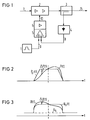
- pulse formation with a control loop according to FIG. 1 is not possible with such RF power amplifiers with a non-linear control characteristic.
- a strong non-linear distortion of the output pulse shape does not only occur in the "pulse foot".
- the output power as a function of time is zero until the modulation control voltage has reached the value of the "starting voltage" of the amplifier.
- This effect causes a time delay between the rising edges of the modulation control pulse and the output pulse.
- the resulting dead time of the amplifier increases the slower the modulation control voltage rises as a function of time.
- the output pulse shape therefore shortens, which cannot be corrected by an arbitrarily fast control algorithm, since the detected controlled variable is zero during the dead time.
- the object of the invention is to provide a measure for the modulation device of an RF power amplifier, which ensures that even with pulse formats in which the time between the transmission of two transmission pulses is extremely short and no longer period of time for adapting the output pulses to the desired one If the desired pulse shape is available, the RF output pulse of the RF power amplifier has this predetermined pulse shape almost undistorted.
- the invention is based on linearizing the RF power amplifier with its modulation control stage as a controlled system. For the reason already explained, this linearization is not realized as a control process with negative feedback, but as a control process.
- the RF amplifier is linearized in such a way that a correction of the modulation pulse is determined from the nonlinear control characteristic so that the effect on the desired output pulse shape and power caused by the nonlinear control characteristic is initially compensated for without intervention by the controller. In terms of control technology, this corresponds to linearization around a fixed operating state, this fixed value denoting the desired operating state of the system.
- the desired pulse shape P o (t) corresponds to a pulse shape U o (t) of the modulation control voltage without interference (FIG. 3). If disturbances acting on the amplifier (e.g. temperature and frequency changes or aging effects) cause changes in the control characteristic or RF amplification and consequently deviations in the pulse shape and power, it is the task of the control system to compensate for these deviations during the pulse transmission and the modulation control voltage U o (t) in the sense of negative feedback to change ⁇ U (t) so that the deviation ⁇ P (t) is reduced.
- This behavior of the control system is shown by way of example in FIGS. 2 and 3 for a trapezoidal envelope pulse P o (t) and a modulation control pulse U o (t) corresponding to a quadratic characteristic of the RF amplifier with a "starting voltage" U s .
- the desired pulse 9 emitted by the pulse generator 1 is corrected in a linearization circuit 11 in accordance with the control characteristic of the RF power amplifier 2 and supplied as a control pulse 12 to the modulation input of the RF power amplifier 2 via a first input of a summing amplifier 13.
- an unavoidable signal delay (“modulator delay”) ⁇ m occurs on the way between the modulation control pulse 10 and the output envelope curve pulse 15.
- the controlled variable (actual pulse 8) is still zero, and there is a pure control process of the output pulse by the modulation control pulse 10.
- the setpoint / actual value comparison in a differential amplifier of the modulator forming the comparator 5 can only take place after the modulator running time ⁇ m with the reference pulse 16 delayed by the same running time in a runtime element 14. The control process therefore only begins with the time delay ⁇ m.
- the output signal of the differential amplifier 5 (control deviation) is evaluated in an evaluation circuit 6 (controller) with a control algorithm and from there it is fed to the summing amplifier 13 via the second input; in the summing amplifier 13 it is then added to the control pulse 12 at the first input.
- the aim is to obtain a high control accuracy on the one hand and a short response time of the control circuit in view of the inevitable modulator running time ⁇ m.
- the control accuracy can be increased if the gain of the controller is increased to low frequencies. This requirement is met by a regulator circuit that has an output voltage of the form supplies (PI controller).
- PI controller proportional gain
- X d : control deviation
- T i : integration time.
- the integral component drastically reduces the response time of the control loop. This is due to the fact that the maximum possible proportional gain of a P-controller (because of the stability problems that occur) is so low that the full control of the controlled system is not achieved even with large deviations. If an integral component is present, the output voltage quickly sums up in the event of larger deviations so that the controlled system is fully controlled. An integral component can therefore also be advantageous if it is not a high adjustment accuracy that is important but a short response time.
- the controller characteristic must be dimensioned with regard to the modulator running time ⁇ m. As a result of the modulator running time, a correction of the modulation control pulse has a delayed effect on the output pulse, as a result of which the control loop can behave unstably.
- the integration time T i of the PI controller is to be dimensioned at least equal to the modulator running time ⁇ m and should be at most about 1 decade above ⁇ m. This makes the cut-off frequency ⁇ 2 of the PI controller, at which the integration effect of the circuit changes into a proportional transmission behavior, comparable to the reciprocal of the modulator runtime.
- the gain of the PI controller at high frequencies must be dimensioned with regard to the reference pulse shape so that the controller can bring control deviations to zero quickly enough.
- a control circuit according to FIG. 5 can advantageously be used.
- An operational amplifier 17 is provided, the input signal being input at its + input via a resistor capacitor network R1, R2, C and the negative feedback from the output via a resistor voltage divider network R3, R4, R5 is.
- the selected implementation corresponds in the transmission behavior of the ideal PI controller with the two restrictions that above the cutoff frequency ⁇ 3 the band limitation by the operational amplifier used (superimposed low-pass behavior) and below the cutoff frequency ⁇ 1 the gain of the controller is limited to a constant value. This measure was introduced in order to limit the loop gain of the control loop in the quasi-stationary state, for example during the pulse roof with trapezoidal target pulses, with regard to the modulation range of the controller.
- the control can not only effectively correct the peak value of the power, but also the course of the edges and the pulse width in the sense of the reference pulse.
Landscapes
- Physics & Mathematics (AREA)
- Nonlinear Science (AREA)
- Engineering & Computer Science (AREA)
- Power Engineering (AREA)
- Amplifiers (AREA)
Claims (6)
- Dispositif de modulation pour un amplificateur de puissance haute fréquence (2) muni d'un ou de plusieurs transistors de puissance haute fréquence, une petite partie du signal de sortie haute fréquence amplifié et modulé de cet amplificateur en étant découplée et démodulée et cette partie étant comparée, en tant qu'impulsion réelle d'enveloppe, avec l'impulsion de modulation de consigne, qui est fournie par un générateur d'impulsions (1), dans un comparateur (5), dont le résultat de comparaison est utilisé pour la modulation en tant qu'impulsion de commande de modulation,
caractérisé par le fait que,
le générateur d'impulsions (1), dans une branche de sortie secondaire, est connecté à un circuit de linéarisation (11), dans lequel l'impulsion de consigne (9) qui est fournie par le générateur d'impulsions est corrigée en fonction de la caractéristique de commande de l'amplificateur de puissance haute fréquence (2), que l'impulsion (12) corrigée dans le circuit de linéarisation est envoyée en tant qu'impulsion de commande à une première entrée d'un amplificateur sommateur (13), dont la deuxième entrée reçoit le résultat de comparaison venant du comparateur (5) par l'intermédiaire d'un circuit de pondération (6), qui effectue, comme un régulateur, une pondération par un algorithme de régulation, que l'impulsion de consigne (9) extraite du générateur d'impulsions passe, sur son chemin menant au comparateur, par un circuit à retard (14), dont le temps de retard correspond au temps (τm) de retard des signaux, dû surtout aux transistors de puissance haute fréquence dans l'amplificateur de puissance haute fréquence, de l'impulsion de commande de modulation (10) à l'impulsion réelle d'enveloppe de sortie (8) de l'amplificateur de puissance haute fréquence, et que le signal de sortie de l'amplificateur sommateur est envoyé en tant qu'impulsion de commande de modulation (10) à l'amplificateur de puissance haute fréquence. - Dispositif de modulation selon la revendication 1,
caractérisé par le fait que,
le circuit de pondération (6) effectue l'algorithme de régulation d'un régulateur proportionnel intégral (PI). - Dispositif de modulation selon la revendication 2,
caractérisé par le fait que,
le temps d'intégration du régulateur PI (6) est au moins aussi long que le temps (τm) de retard des signaux et qu'il se situe au maximum environ une décade au-dessus du temps (τm) de retard des signaux. - Dispositif de modulation selon l'une des revendications 1 à 3,
caractérisé par le fait que,
l'impulsion de consigne (9) peut être extraite d'une mémoire programmable servant à des signaux numériques. - Dispositif de modulation selon l'une des revendications précédentes,
caractérisé par le fait que,
aussi bien l'impulsion de commande (12) que l'impulsion de référence (16) retardée sont extraites chacune d'une mémoire programmable pour des signaux numériques. - Dispositif de modulation selon la revendication 1,
caractérisé par le fait que,
l'on prévoit en tant que comparateur (5) un amplificateur de différence.
Applications Claiming Priority (2)
| Application Number | Priority Date | Filing Date | Title |
|---|---|---|---|
| DE4038534 | 1990-12-03 | ||
| DE4038534 | 1990-12-03 |
Publications (2)
| Publication Number | Publication Date |
|---|---|
| EP0489276A1 EP0489276A1 (fr) | 1992-06-10 |
| EP0489276B1 true EP0489276B1 (fr) | 1995-06-28 |
Family
ID=6419500
Family Applications (1)
| Application Number | Title | Priority Date | Filing Date |
|---|---|---|---|
| EP91119268A Expired - Lifetime EP0489276B1 (fr) | 1990-12-03 | 1991-11-12 | Dispositif de modulation pour un amplificateur de puissance haute fréquence |
Country Status (4)
| Country | Link |
|---|---|
| US (1) | US5194823A (fr) |
| EP (1) | EP0489276B1 (fr) |
| DE (1) | DE59105864D1 (fr) |
| ES (1) | ES2073647T3 (fr) |
Families Citing this family (34)
| Publication number | Priority date | Publication date | Assignee | Title |
|---|---|---|---|---|
| JP2710503B2 (ja) * | 1991-10-14 | 1998-02-10 | 日本電気株式会社 | 出力電力制御回路 |
| US5473461A (en) * | 1994-08-26 | 1995-12-05 | Interactive Light, Inc. | Wide dynamic range optical receiver |
| JP2571033B2 (ja) * | 1994-12-30 | 1997-01-16 | 日本電気株式会社 | 送信電力増幅回路の出力制御回路 |
| DE19506051C2 (de) * | 1995-02-22 | 1999-07-29 | Mikom Gmbh | Schaltungsanordnung zur Reduzierung der Amplitude von Intermodulationsprodukten |
| JPH09331222A (ja) * | 1996-06-11 | 1997-12-22 | Nec Corp | 利得制御信号補正装置 |
| US20050000876A1 (en) * | 1999-12-03 | 2005-01-06 | Knight Steven R. | Keyed latch valve for fuel filter |
| GB2359681B (en) * | 2000-02-25 | 2004-03-10 | Wireless Systems Int Ltd | Switched amplifier |
| GB2386012A (en) * | 2002-03-02 | 2003-09-03 | Motorola Inc | A linearized class C RF amplifier |
| US7031672B2 (en) * | 2003-03-24 | 2006-04-18 | Quorum Systems, Inc. | Direct conversion transmitter system and method with quadrature balancing and low LO feed through |
| US7031688B2 (en) | 2003-03-24 | 2006-04-18 | Quorum Systems, Inc. | Direct-conversion receiver system and method with quadrature balancing and DC offset removal |
| JP4707319B2 (ja) * | 2003-11-19 | 2011-06-22 | 株式会社東芝 | パルス電力増幅器 |
| JP4298705B2 (ja) * | 2004-01-16 | 2009-07-22 | 三菱電機株式会社 | 電力供給装置及び電力供給方法 |
| DE102004038089B4 (de) * | 2004-08-05 | 2016-02-04 | Rohde & Schwarz Gmbh & Co. Kg | Reglergestütztes Verfahren und reglergestützte Vorrichtung zur Bestimmung der Kennlinie eines Kompensationsgliedes in einem Pegelkreis |
| US7683827B2 (en) * | 2004-12-15 | 2010-03-23 | Valeo Radar Systems, Inc. | System and method for reducing the effect of a radar interference signal |
| US7403153B2 (en) * | 2004-12-15 | 2008-07-22 | Valeo Raytheon Systems, Inc. | System and method for reducing a radar interference signal |
| US7038608B1 (en) * | 2004-12-16 | 2006-05-02 | Valeo Raytheon Systems, Inc. | Digital to analog converter |
| US7603097B2 (en) * | 2004-12-30 | 2009-10-13 | Valeo Radar Systems, Inc. | Vehicle radar sensor assembly |
| US7680464B2 (en) * | 2004-12-30 | 2010-03-16 | Valeo Radar Systems, Inc. | Waveguide—printed wiring board (PWB) interconnection |
| US7248215B2 (en) * | 2004-12-30 | 2007-07-24 | Valeo Raytheon Systems, Inc | Beam architecture for improving angular resolution |
| US20070156799A1 (en) * | 2005-12-30 | 2007-07-05 | Gilbert Michael J | Multi-stage finite impulse response filter processing |
| US7345619B2 (en) * | 2005-12-30 | 2008-03-18 | Valeo Raytheon Systems, Inc. | Generating event signals in a radar system |
| US7400290B2 (en) * | 2005-12-30 | 2008-07-15 | Valeo Raytheon Systems, Inc. | Vehicle radar system having multiple operating modes |
| US7336219B1 (en) | 2005-12-30 | 2008-02-26 | Valeo Raytheon Systems, Inc. | System and method for generating a radar detection threshold |
| US7379018B1 (en) | 2005-12-30 | 2008-05-27 | Valeo Raytheon Systems, Inc. | System and method for verifying a radar detection |
| US20070152874A1 (en) * | 2005-12-30 | 2007-07-05 | Woodington Walter G | Reducing undesirable coupling of signal(s) between two or more signal paths in a radar system |
| US20070152872A1 (en) * | 2005-12-30 | 2007-07-05 | Woodington Walter G | Reducing undesirable coupling of signal(s) between two or more signal paths in a radar system |
| US20070152869A1 (en) * | 2005-12-30 | 2007-07-05 | Woodington Walter G | Multichannel processing of signals in a radar system |
| US20100238066A1 (en) * | 2005-12-30 | 2010-09-23 | Valeo Raytheon Systems, Inc. | Method and system for generating a target alert |
| US20080001809A1 (en) * | 2006-06-30 | 2008-01-03 | Walter Gordon Woodington | Detecting signal interference in a vehicle system |
| TWM349649U (en) * | 2008-09-10 | 2009-01-21 | Amazing Microelectronic Corp | Bias balancing circuit |
| DE102011082351A1 (de) * | 2011-09-08 | 2013-03-14 | Rohde & Schwarz Gmbh & Co. Kg | Verfahren und Vorrichtung zur Pegelregelung eines gepulsten Hochfrequenzsignals |
| US9653796B2 (en) | 2013-12-16 | 2017-05-16 | Valeo Radar Systems, Inc. | Structure and technique for antenna decoupling in a vehicle mounted sensor |
| FR3060915B1 (fr) * | 2016-12-15 | 2019-01-25 | Thales | Controle du spectre d'une emission rf impulsionnelle par mise en forme des impulsions |
| CN107707211A (zh) * | 2017-09-27 | 2018-02-16 | 上海联影医疗科技有限公司 | 一种功率放大器功率补偿方法、装置和系统 |
Family Cites Families (7)
| Publication number | Priority date | Publication date | Assignee | Title |
|---|---|---|---|---|
| DE1297703B (de) * | 1966-02-09 | 1969-06-19 | Rohde & Schwarz | Schaltungsanordnung zum Linearisieren der Verstaerkung eines Hochfrequenzverstaerkers fuer Einseitenbandsignale |
| DE2904011C3 (de) * | 1979-02-02 | 1981-11-26 | SIEMENS AG AAAAA, 1000 Berlin und 8000 München | Hochfrequenzimpulsverstärker |
| JPS5999851A (ja) * | 1982-11-29 | 1984-06-08 | Nec Corp | 信号制御回路 |
| US4706262A (en) * | 1984-03-30 | 1987-11-10 | Nec Corporation | FSK or FM burst signal generating apparatus |
| US4561111A (en) * | 1984-08-06 | 1985-12-24 | Rockwell International Corporation | Method of predistorting a single sideband system |
| CH671120A5 (fr) * | 1986-11-20 | 1989-07-31 | Bbc Brown Boveri & Cie | |
| US4939483A (en) * | 1989-10-31 | 1990-07-03 | John Fluke Mfg. Co., Inc. | Modulation frequency response stabilized amplitude modulation circuit |
-
1991
- 1991-11-12 DE DE59105864T patent/DE59105864D1/de not_active Expired - Fee Related
- 1991-11-12 EP EP91119268A patent/EP0489276B1/fr not_active Expired - Lifetime
- 1991-11-12 ES ES91119268T patent/ES2073647T3/es not_active Expired - Lifetime
- 1991-12-03 US US07/802,047 patent/US5194823A/en not_active Expired - Fee Related
Also Published As
| Publication number | Publication date |
|---|---|
| US5194823A (en) | 1993-03-16 |
| DE59105864D1 (de) | 1995-08-03 |
| ES2073647T3 (es) | 1995-08-16 |
| EP0489276A1 (fr) | 1992-06-10 |
Similar Documents
| Publication | Publication Date | Title |
|---|---|---|
| EP0489276B1 (fr) | Dispositif de modulation pour un amplificateur de puissance haute fréquence | |
| DE69024182T2 (de) | Linearer sender | |
| DE69216931T2 (de) | Übertrager mit Nichtlinearitätskorrekturkreisen | |
| DE19860097B4 (de) | Schaltungseinrichtung, Verfahren zum Bereitstellen eines linearen Leistungsverstärkers und Verwendung einer Schaltungseinrichtung | |
| DE69129340T2 (de) | Leistungsverstärker mit verschiedenen geschalteten Stufen | |
| DE69317866T2 (de) | Verzerrungskompensationsschaltung von Hochfrequenzleistungsverstärker | |
| DE3516603C2 (fr) | ||
| EP1260016B1 (fr) | Procede et circuit d'emission permettant de generer un signal d'emission | |
| DE60001071T2 (de) | Verfahren und vorrichtung zur linearisierung eines verstärkers | |
| DE2758933C3 (de) | Linearer Transistor-Leistungsverstärker | |
| EP1195005B1 (fr) | Dispositif et procede pour effectuer une predistorsion d'un signal de transmission a transmettre sur une ligne de transmission non lineaire | |
| DE69901704T2 (de) | Kompensationsverfahren von nichtlinearitäten in einem verstärker, verstärker sowie verwendung des verfahrens und des verstärkers | |
| DE2519845B2 (de) | Schaltungsanordnung zur zusammenfuehrung von hochfrequenzleistungsanteilen | |
| DE2147167A1 (de) | Vorrichtung zur Verringerung der Zwischenmodulation | |
| DE60313036T2 (de) | Signaljustierung basierend auf phasenfehler | |
| EP0635936B1 (fr) | Système de communication utilisant des signaux selon le système de multiplexage par répartition dans le temps | |
| EP0462304B1 (fr) | Montage de réglage en amplitude d'un oscillateur | |
| DE1156844B (de) | Saegezahnspannungsgenerator, insbesondere zur zeitlinearen Ablenkung des Abtastflecks von Elektronenstrahlen | |
| EP1203447B1 (fr) | Procede et dispositif pour faire fonctionner un amplificateur de puissance hf | |
| DE2624337C2 (de) | Doppelgegentaktmodulator mit einem Gegentaktverstärker | |
| DE3034950A1 (de) | Sender fuer impulsfoermige hf-signale | |
| DE4316526A1 (de) | Sender mit einem steuerbaren Leistungsverstärker | |
| DE947807C (de) | Nichtlinearer symmetrischer Vierpol | |
| DE60020896T2 (de) | Linearisierungsschaltung und Verfahren, insbesondere für Mikrowellenfunksysteme | |
| DE2917020C3 (de) | Lineare, transistorisierte Wechselstrom-Verstärker-Schaltung |
Legal Events
| Date | Code | Title | Description |
|---|---|---|---|
| PUAI | Public reference made under article 153(3) epc to a published international application that has entered the european phase |
Free format text: ORIGINAL CODE: 0009012 |
|
| AK | Designated contracting states |
Kind code of ref document: A1 Designated state(s): BE DE ES FR GB IT |
|
| 17P | Request for examination filed |
Effective date: 19920807 |
|
| 17Q | First examination report despatched |
Effective date: 19940822 |
|
| GRAA | (expected) grant |
Free format text: ORIGINAL CODE: 0009210 |
|
| AK | Designated contracting states |
Kind code of ref document: B1 Designated state(s): BE DE ES FR GB IT |
|
| REF | Corresponds to: |
Ref document number: 59105864 Country of ref document: DE Date of ref document: 19950803 |
|
| REG | Reference to a national code |
Ref country code: ES Ref legal event code: FG2A Ref document number: 2073647 Country of ref document: ES Kind code of ref document: T3 |
|
| ITF | It: translation for a ep patent filed | ||
| GBT | Gb: translation of ep patent filed (gb section 77(6)(a)/1977) |
Effective date: 19950907 |
|
| ET | Fr: translation filed | ||
| PLBE | No opposition filed within time limit |
Free format text: ORIGINAL CODE: 0009261 |
|
| STAA | Information on the status of an ep patent application or granted ep patent |
Free format text: STATUS: NO OPPOSITION FILED WITHIN TIME LIMIT |
|
| 26N | No opposition filed | ||
| REG | Reference to a national code |
Ref country code: GB Ref legal event code: 732E |
|
| REG | Reference to a national code |
Ref country code: FR Ref legal event code: TP |
|
| PGFP | Annual fee paid to national office [announced via postgrant information from national office to epo] |
Ref country code: GB Payment date: 19991027 Year of fee payment: 9 |
|
| PGFP | Annual fee paid to national office [announced via postgrant information from national office to epo] |
Ref country code: ES Payment date: 19991118 Year of fee payment: 9 |
|
| PGFP | Annual fee paid to national office [announced via postgrant information from national office to epo] |
Ref country code: FR Payment date: 19991123 Year of fee payment: 9 Ref country code: BE Payment date: 19991123 Year of fee payment: 9 |
|
| PGFP | Annual fee paid to national office [announced via postgrant information from national office to epo] |
Ref country code: DE Payment date: 20000320 Year of fee payment: 9 |
|
| PG25 | Lapsed in a contracting state [announced via postgrant information from national office to epo] |
Ref country code: GB Free format text: LAPSE BECAUSE OF NON-PAYMENT OF DUE FEES Effective date: 20001112 |
|
| PG25 | Lapsed in a contracting state [announced via postgrant information from national office to epo] |
Ref country code: ES Free format text: LAPSE BECAUSE OF NON-PAYMENT OF DUE FEES Effective date: 20001113 |
|
| PG25 | Lapsed in a contracting state [announced via postgrant information from national office to epo] |
Ref country code: BE Free format text: LAPSE BECAUSE OF NON-PAYMENT OF DUE FEES Effective date: 20001130 |
|
| BERE | Be: lapsed |
Owner name: DAIMLER-BENZ A.G. Effective date: 20001130 |
|
| GBPC | Gb: european patent ceased through non-payment of renewal fee |
Effective date: 20001112 |
|
| PG25 | Lapsed in a contracting state [announced via postgrant information from national office to epo] |
Ref country code: FR Free format text: LAPSE BECAUSE OF NON-PAYMENT OF DUE FEES Effective date: 20010731 |
|
| PG25 | Lapsed in a contracting state [announced via postgrant information from national office to epo] |
Ref country code: DE Free format text: LAPSE BECAUSE OF NON-PAYMENT OF DUE FEES Effective date: 20010801 |
|
| REG | Reference to a national code |
Ref country code: FR Ref legal event code: ST |
|
| REG | Reference to a national code |
Ref country code: ES Ref legal event code: FD2A Effective date: 20011214 |
|
| PG25 | Lapsed in a contracting state [announced via postgrant information from national office to epo] |
Ref country code: IT Free format text: LAPSE BECAUSE OF NON-PAYMENT OF DUE FEES;WARNING: LAPSES OF ITALIAN PATENTS WITH EFFECTIVE DATE BEFORE 2007 MAY HAVE OCCURRED AT ANY TIME BEFORE 2007. THE CORRECT EFFECTIVE DATE MAY BE DIFFERENT FROM THE ONE RECORDED. Effective date: 20051112 |