EP0489944A1 - Procédé de communication de données maître-esclave avec bus flexible à un câble - Google Patents
Procédé de communication de données maître-esclave avec bus flexible à un câble Download PDFInfo
- Publication number
- EP0489944A1 EP0489944A1 EP90123647A EP90123647A EP0489944A1 EP 0489944 A1 EP0489944 A1 EP 0489944A1 EP 90123647 A EP90123647 A EP 90123647A EP 90123647 A EP90123647 A EP 90123647A EP 0489944 A1 EP0489944 A1 EP 0489944A1
- Authority
- EP
- European Patent Office
- Prior art keywords
- address
- data
- slave
- telegram
- wire bus
- Prior art date
- Legal status (The legal status is an assumption and is not a legal conclusion. Google has not performed a legal analysis and makes no representation as to the accuracy of the status listed.)
- Granted
Links
- 238000000034 method Methods 0.000 title description 3
- 230000005540 biological transmission Effects 0.000 claims abstract description 32
- 230000015654 memory Effects 0.000 claims description 36
- 238000012360 testing method Methods 0.000 claims description 14
- 230000000903 blocking effect Effects 0.000 claims description 11
- 238000012545 processing Methods 0.000 claims description 8
- 230000001360 synchronised effect Effects 0.000 claims description 3
- 230000007704 transition Effects 0.000 claims description 3
- 238000011156 evaluation Methods 0.000 claims 1
- 230000002123 temporal effect Effects 0.000 claims 1
- 238000012546 transfer Methods 0.000 abstract description 4
- 230000006870 function Effects 0.000 description 9
- 230000008901 benefit Effects 0.000 description 7
- 238000010586 diagram Methods 0.000 description 7
- 238000005259 measurement Methods 0.000 description 5
- 238000005516 engineering process Methods 0.000 description 4
- 230000001419 dependent effect Effects 0.000 description 2
- 238000013461 design Methods 0.000 description 2
- 125000000524 functional group Chemical group 0.000 description 2
- 230000008569 process Effects 0.000 description 2
- 230000004913 activation Effects 0.000 description 1
- 230000008859 change Effects 0.000 description 1
- 230000008878 coupling Effects 0.000 description 1
- 238000010168 coupling process Methods 0.000 description 1
- 238000005859 coupling reaction Methods 0.000 description 1
- 238000001514 detection method Methods 0.000 description 1
- 230000010354 integration Effects 0.000 description 1
- 238000009420 retrofitting Methods 0.000 description 1
Images

Classifications
-
- H—ELECTRICITY
- H04—ELECTRIC COMMUNICATION TECHNIQUE
- H04L—TRANSMISSION OF DIGITAL INFORMATION, e.g. TELEGRAPHIC COMMUNICATION
- H04L12/00—Data switching networks
-
- H—ELECTRICITY
- H04—ELECTRIC COMMUNICATION TECHNIQUE
- H04L—TRANSMISSION OF DIGITAL INFORMATION, e.g. TELEGRAPHIC COMMUNICATION
- H04L12/00—Data switching networks
- H04L12/28—Data switching networks characterised by path configuration, e.g. LAN [Local Area Networks] or WAN [Wide Area Networks]
- H04L12/40—Bus networks
- H04L12/403—Bus networks with centralised control, e.g. polling
-
- H—ELECTRICITY
- H04—ELECTRIC COMMUNICATION TECHNIQUE
- H04L—TRANSMISSION OF DIGITAL INFORMATION, e.g. TELEGRAPHIC COMMUNICATION
- H04L12/00—Data switching networks
- H04L12/28—Data switching networks characterised by path configuration, e.g. LAN [Local Area Networks] or WAN [Wide Area Networks]
- H04L12/40—Bus networks
- H04L12/407—Bus networks with decentralised control
- H04L12/413—Bus networks with decentralised control with random access, e.g. carrier-sense multiple-access with collision detection [CSMA-CD]
- H04L12/4135—Bus networks with decentralised control with random access, e.g. carrier-sense multiple-access with collision detection [CSMA-CD] using bit-wise arbitration
Definitions
- the invention relates to a master-slave data transmission system with a master that sends data to or retrieves data from a slave, the data being transferred via a single-wire bus by means of a telegram that contains the following subsections: an address part that stores the data sink or defines the data source in the slave, a data part that contains either the sent or the retrieved data and finally start and end information, cf. the preamble of claim 1.
- Such a master-slave data transmission system with a single-wire bus is known per se, for example in the field of telecontrol technology with a single data transmission channel.
- the conflict-free control of the single-wire bus requires an elaborate control circuit, which can only be accepted if additional bus and control lines must be avoided due to the distance.
- the progress in integration technology especially in monolithically integrated circuit technology, has made it possible to equip components that were previously regarded as passive with "electronic intelligence". This can also lead to great advantages in data transmission systems where the distance point of view is less critical, as will be shown.
- the flexibility of the master-slave data transmission system with the single-wire bus essentially results from the fact that the individual elements of the data format can vary from telegram to telegram, both in number and in themselves.
- a further advantage results in data transmission systems which contain such masters and slaves as interchangeable components.
- An application is found, for example, in the motor vehicle sector when one or more processors serving as masters have to call up data from spatially separated sensors that serve as slaves.
- the freely selectable address length also makes replacement or retrofitting easier. This is because new, additional functions that can be called up via longer addresses as so-called options do not conflict with previous functions because they can still be called up via the previous, shorter addresses.
- Another advantage results from the saving of connecting legs in the case of independent components which are coupled together in such a system.
- the number of connection legs of "intelligent" sensors, memories, transmitters etc. can be reduced to three.
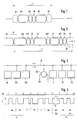
- the telegram T begins with start information si. This is followed by an address part ad variable in length, a first label m1, a synchronization bit sb, a part dt variable in length and finally an end information item oi.
- the single-wire bus B (cf. FIG. 3) assumes an idle or waiting state. In the idle state, the single-wire bus is either switched to high impedance or set to an upper or lower switching potential, cf. also Fig. 4. Outside the telegram T, a bit clock bt can be transmitted as a waiting signal on the single-wire bus. In this case, the transmission of special bits for the start and end information si, oi can be omitted.
- the start information si is defined by the last bit clock period and the end information oi by two immediately consecutive bit clock periods.
- the first mark is expediently ml and that Synchronizing bit sb also only lasts for one bit clock period.
- FIG. 4 shows how the individual signals can be distinguished using different duty cycles.
- FIG. 2 schematically shows a more complex telegram T, which however contains all the elements known from FIG. 1.
- the master constantly sends the bit clock bt via the single-wire bus.
- the end of the bit clock bt and the start of the data of the address part ad form the start information si.
- the address part ad is followed by the first mark m1, the synchronization bit sb and the data part dt, which is variable in length.
- a second mark m2 indicates that the telegram T has not yet ended.
- test part tx also variable in length, a third mark m3, a blocking bit bb and finally the final information oi.
- the test part tx is used to check the address part ad and / or data part dt. When an error is detected, the logical state of the blocking bit bb is changed, which triggers the invalidity of the entire transmitted telegram T.
- the address part ad - also in the format of FIG. 1 - can be split into a device address, an internal address in general and an operation address. Different slaves are addressed using the device address.
- the internal address ia allows access to different data sources or data sinks within a slave.
- the operation address or the like determines which operation the slave should perform in detail. If the slave is a read-write memory, for example, then this memory can be prepared for the write or read operation by means of the special operation address or the like.
- the synchronization bit sb in FIGS. 1 and 2 serves to indicate to the master that the slave is currently not ready to accept the telegram T that has started.
- the master then releases the single-wire bus by sending the end information oi and, if necessary, sends the telegram T again after a waiting time.
- the recognition of the start information si suppresses the transmission of own telegrams T until the end information oi appears on the single-wire bus. If several masters coincidentally begin to send telegrams T, then those masters which "determine” a difference between the bit sent and received in each case by means of an output error detector af (cf. FIG. 5) "say goodbye". This is possible because the single-wire bus is designed as a "wired-OR" link. One of the two switching states, usually the L switching state, must already be enforced by a single master or a single slave. In the same way, the logical state of the synchronization bit sb and the block kier bit bb is changed within the respective bit period. The priority control of the single-wire bus is thus carried out in a simple manner by the output error detector af.
- the active master If the active master sends its bit clock bt in the waiting state after sending its telegram, it shapes all other masters and slaves Bit clock until a new master can be identified by start information si and henceforth takes over the clock management.
- the duty cycle in which the bit clock bt is sent during the wait state depends on how the first address bit is recognized. A logical "0", "1" or a label may have to be inserted as start information si before the first address bit.
- a master can send data to a slave via the single-wire bus B or retrieve data from there.
- the individual slaves can be distinguished by different device addresses. If data should also be exchangeable between the masters, the addressable masters must be addressable and addressable like a slave.
- a slave S3 is shown as a tripod element, two connections being provided for the supply voltages and the third connection being connected to the single-wire bus B.
- Such a component is, for example, an electronic temperature sensor, the digitized temperature value of which is called up via the single-wire bus.
- FIG. 4 schematically shows a section of the time profile of a telegram T with the associated bit clock bt. Only the clock periods are marked by the bit clock bt because the actual signal curve, that is to say the pulse duty factor, is in itself arbitrary.
- the signal curve of some bit clock periods of the telegram T is shown under the bit clock bt.
- bit clock bt At the beginning of each bit clock period there is a transition from the L to the H switching state.
- the negative switching edge occurs and is defined at certain times during the bit clock period H and L switching states of different lengths within the bit clock.
- a first or second H / L duty cycle which is smaller or larger than 1, defines a logical "0" or "1".
- a third H / L duty cycle defines the mark mi and possibly also the bit clock bt during the waiting state.
- the transition from the bit clock bt or from the marks mi to a data bit "0" or "1" characterizes the start information si.
- the end information oi is recognized if at least two marks mi are sent in succession.
- the synchronization bit sb and the blocking bit bb are characterized by the fact that a first logic state, e.g. a "1" is sent. If the slave is ready for further processing of the telegram T, it maintains the logical state of the synchronization bit sb or the blocking bit bb.
- the slave If, however, the slave is not ready for further processing of the telegram T, it triggers by transcoding the synchronization bit into a second logic state, e.g. a "0", in the master M a non-ready signal. Similarly, if a fault is detected, the slave triggers by recoding the blocking bit bb into the second logic state, e.g. "0", in the master M an invalid signal. In both cases, the telegram sent is ineffective, so that it must be repeated later. This assignment applies to the "wired-OR" link, in which a "0" prevails over the "1".
- the required duty cycle is easiest to derive from an internal system clock cl or auxiliary clock ht (see FIGS. 5 and 6), the frequency of which is at least twice the bit clock bt.
- the positive edges of the telegram T supply the exact bit clock bt that is in the slaves and possibly in Connect all auxiliary clock and clock generators to the other masters with phase accuracy using phase locked loops.
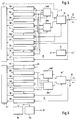
- FIG. 5 shows the individual functional groups of a master M schematically. Since the function groups represent circuits familiar to the person skilled in the art, a more detailed illustration and description is unnecessary for better clarity.
- the timing and the control of the individual function groups is undertaken by a master control device st, which receives control signals from the individual function groups or sends control signals for their activation.
- An input-output stage io is connected with its output terminal k to the single-wire bus B and generates the individual H and L switching signals in transmit mode.
- the switching states of the single-wire bus B are sensed and a decoder dec is fed. Any changeover of the input / output stage io to a high-resistance tristate state is provided by a signal on the control line f shown in dashed lines.
- the decoder dec for the received signals corresponds to the encoder cod for the signals to be transmitted - it controls the pulse duty factor of the transmitted bits.
- the decoder dec decodes the received signals with respect to their duty cycle.
- the corresponding windows are formed by a duty cycle control tr, which is connected to the control inputs of the encoder and decoder.
- the duty cycle control tr also controls a mark generator mg, which forms the mark mi for the single-wire bus B directly via the input-output stage io.
- the serial input data for the encoder cod come either from an address generator ag, a data source dq or a test data generator tg.
- the serial output data of the Decoders dec are either fed to a data sink ds, the test data generator tg or a stop signal detector sd, the comparison input of which is fed by the mark generator mg.
- the stop signal detector sd detects a significant difference in the pulse duty factor between the two supplied signals, then it signals the master control device st to recognize the readiness signal or the invalid signal.
- An error detector fg works in a similar manner, which is fed at one input with the output data of the test data generator tg and at the other input with the output data of the decoder dec.
- the test data are formed from the address data and / or the sent or received data, which are fed to the test data generator for billing. If the same calculation of the data as test data takes place in slave S, then a faulty transmission is recognized by comparing the test data with the test data received by means of the error detector fd.
- an output error detector af the first data input of which is connected to the output of the encoder cod and the second data input of which is connected to the output terminal k of the input-output stage io.
- a clock generator tc is shown as a separate block, which generates an internal system clock c1 and whose internal phase-locked loop (not shown) is coupled to the single-wire bus B or is fed by an external system clock cl '.
- the supply of the single-wire bus B during the waiting state with the bit clock bt is done by the mark generator mg.
- the presence of all function groups in the Master M is not necessary for reduced operating tasks. If, for example, only data is to be called up, then the data source dq is omitted.
- the complex test data generator tg which is also required in the slave, is omitted if the required data transmission security is low or can be achieved in some other way, for example by repetition.
- the processing of the data format according to FIG. 1 naturally also does not require a test data generator.
- a slave S with its individual function blocks is shown schematically in FIG. 6.
- the functional similarity to Master M is also expressed in the drawing.
- An input-output stage io ' is connected to the single-wire bus B with its output terminal k'.
- the internal data output of this input-output stage is connected to a decoder dec 'and the internal data input is connected to the output of an encoder cod', which is fed by a data source dq '.
- the output of the decoder dec ' is routed to a data sink ds', an address comparator al with an address length checking device ue and a mark detector md.
- the windows for the different duty cycles in the encoder cod 'and decoder dec' are controlled by a duty cycle controller tr '. This also controls the duty cycle for the non-readiness and invalid signal, which are formed in a stop signal generator sg and are fed directly to the input-output stage io '. There is the second logical state, so "0", the respective synchronization bit sb or blocking bit bb forced.
- bit clock detector bd which, in the absence of the bit clock, triggers a current-saving state via an operating mode switch bu which acts on the slave control device st '.
- an auxiliary clock generator hg is coupled to the bit clock detector bd, the output signal of which is an auxiliary clock ht with a simple integer frequency ratio to the bit clock bt.
- the slave S is implemented in CMOS technology, then only the internal clock must be switched off in order to bring the circuit into a currentless state.
- the address length checking device ue is located in the address comparator a1, to which addresses of any length can be supplied. If the address part ad (or the device address da) and the address length do not match, the transmission of a takeover signal aj (see FIG. 7) does not occur the slave control device st '. Thus, a random address match in addresses of different lengths cannot lead to the transfer.
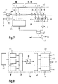
- FIG. 7 shows a block diagram of an exemplary embodiment of an address length checking device ue.It requires very little additional components and essentially consists of the shift register sr, which is present anyway and in which the serially supplied data of the address part ad are stored.
- the shift register contains sr for checking the address length at least n + 1 shift register levels, where n is the number of digits of the address to be recognized.
- a start signal si ' which is derived from the start information si, all shift register stages except for the first are set to "0" at the latest at the start of the writing process; the first shift register level is set to "1".
- the individual shift register stages are set via their set and reset inputs or via their data inputs, to which either a "1" or a "0" is supplied from a first or second memory h1, h2.
- the serial reading of the addresses into the individual shift register stages begins, which continues until the first mark m1 ends the shifting process. If the address length matches, the set "1" of the first shift register stage must in the meantime have been shifted into the (n + 1) th shift register stage.
- the criterion for the correct address length is the check that a first "1" has arrived in the (n + 1) th shift register stage and that this first "1" is still present there.
- the circuit for this check comprises a first and second RS flip-flop f1, f2, two further shift register stages n + 1 and n + 2, an inverter i and finally a first and second AND gate u1, u2.
- the start signal si ' the reset inputs R of the two RS flip-flops f1, f2 are activated at the beginning of the address length measuring interval.
- the set input Set of the first and second RS flip-flops f1, f2 is connected to the output of the (n + 1) th and (n + 2) th shift register stage.
- the Q output of the first and second RS flip-flops f1, f2 is direct with an input of the first AND gate u1 or with one second input connected via the inverter i.
- Another input of the first AND gate is connected to the output of a device address comparator dk, the parallel input of which is fed by those shift register stages which contain the device address da.
- the device address comparator contains the device address to be recognized as hardware
- the switching state of the (n + 1) th shift register stage can of course also be checked in another way. For example, it can be checked whether the first RS flip-flop f1 toggled for the first time with the last bit clock or earlier.
- FIG. 8 schematically shows a multiple data source as a block diagram, which serves as data source dq 'in a slave.
- the actual data source consists of several analog signal sources q1, q2, qi, which are sampled one after the other by a first multiplexer p1 and fed to an analog-digital converter ac. Its output feeds the input of a second multiplexer p2, which writes the data into the memory cells r1, r2, ri of a memory device mr.
- the data dat of the individual memory cells is read out by controlling the respective memory cell using the internal address ia.
- a particularly advantageous application of such master-slave data transmission systems in which the slaves contain a single or a multiple analog signal source as data sources dq ', can be found in all types of sensor components for a wide variety of measurement tasks.
- Their connection via the single-wire bus B enables a large number of identical or different sensor components to be queried via a single single-wire connection.
- the required number of connection legs of the sensor components can be reduced to three connections in extreme cases, cf. Fig. 3 and Fig. 9.
- the first terminal a1 is used to connect to single-wire bus B.
- the second and third connections a2, a3 are used to connect to the positive and negative supply voltages.
- FIG. 9 schematically shows a three-legged sensor component S3, which is connected, for example, to an ohmic position or angle encoder Rx.
- Its unknown resistance can be determined in that the voltage U between the second and third connection legs a2, a3 and the cross current I are called up as data via the single-wire bus B.
- the unknown resistance value Rx can be determined in the master M from the transmitted values U, I and the known supply voltage Ub with the aid of an arithmetic unit connected to the data sink ds in the master M.
- the absolute resistance value of the position transmitter Rx is not important and a relative measurement is sufficient, then it is sufficient if a connected current I1 can be changed in fixed but predetermined steps in sensor S3 or is simply doubled.
- the relative change in resistance of the position transmitter Rx can then be determined from the measured voltage values U without knowing the actual value of the cross current I. This is usually sufficient to reset a certain position or a given angle of rotation, etc.
- the schematic representation according to FIG. 9 contains in addition to those already described in more detail Function groups sj of the slave, a current source switchover device xq and / or a voltage source switchover device xu.
- a device for voltage measurement between the second and third connection legs a2, a3 serves as the analog signal source, but is not shown in FIG. 9.
- FIG. 10 shows another advantageous application for such a master-slave data transmission system with a single-wire bus B, namely a memory component S4 with "built-in intelligence".
- the memory device mr contains an address calculation program which is read into this memory area via a master-slave data transmission system mj according to the invention.
- the output terminal k 'of the slave is the first connection leg a1 of the memory component, which is connected to the single-wire bus B.
- the memory component S4 receives the telegrams T which contain the individual steps of the address computing program in a programming phase.
- these are simple, cyclically repeating computing programs, the individual addresses being determined in an address computing device ap.
- the freely accessible area mf of the memory device mr is connected to a data output stage vo and a data input stage vi. At least one set of connecting legs is available for the output or input data od, id, via which a parallel processing of the data transfer is made possible.
- auxiliary clock ht which is formed by an auxiliary clock generator hg, which is either latched to the bit clock bt or to a call signal sa.
- the data cycle is also synchronized with the external call signal sa whose period is a simple integer multiple of the auxiliary clock ht or the bit clock bt.
- the synchronism between the different clocks is achieved in the usual way by means of a phase locked loop in the auxiliary clock generator hg.
- Such a memory component S4 with built-in address calculation is particularly advantageous where the read and write rate and the required number of connecting legs are very high.
- Such a memory is required, for example, for the frame storage of color television signals for image signal processing.
- the housing expenditure for multi-legged memory components is very high. As a rule, the length increases with the number of connecting legs. This results in a stronger coupling of the signals to one another, which limits the data rate.
- the invention provides a very substantial remedy here because such fast components now do completely without address legs.
- FIG. 11 Another advantageous type of memory component S5 is shown in FIG. 11. This is a pure tripod arrangement, the first connection a1 of which is connected to the single-wire bus B, while the first and third connection legs are connected to the positive and negative supply voltages.
- Such three-legged memory components S5 can be used where a low data transfer rate is sufficient. The serial processing of the entire data transmission process can then easily take place via the single-wire bus B.
- the respective internal address in the memory component S5, which contains, for example, adjustment or setting data for a picture tube, can be controlled via the internal address part ia in the telegram T. If the stored data is not changed during operation, this is simplified Storage device for a read-only memory.
- An advantage of these three-legged components is that inexpensive three-legged transistor housings can be used.
- the slow processing of the telegram T on the single-wire bus B also does not require an actual master M as a component, but can be replaced by a functionally identical processing program that is loaded as software into a commercially
Landscapes
- Engineering & Computer Science (AREA)
- Computer Networks & Wireless Communication (AREA)
- Signal Processing (AREA)
- Small-Scale Networks (AREA)
- Information Transfer Systems (AREA)
Priority Applications (6)
| Application Number | Priority Date | Filing Date | Title |
|---|---|---|---|
| DE59009700T DE59009700D1 (de) | 1990-12-08 | 1990-12-08 | Master-Slave-Datenübertragungsverfahren mit flexiblem Eindraht-Bus. |
| EP90123647A EP0489944B1 (fr) | 1990-12-08 | 1990-12-08 | Procédé de communication de données maître-esclave avec bus flexible à un câble |
| US07/796,728 US5237322A (en) | 1990-12-08 | 1991-11-22 | Master-slave data transmission system employing a flexible single-wire bus |
| KR1019910022457A KR0161668B1 (ko) | 1990-12-08 | 1991-12-07 | 단일 가요성 와이어 버스를 갖는 마스터-슬레이브 데이타 전송 시스템 |
| JP3324612A JP2954410B2 (ja) | 1990-12-08 | 1991-12-09 | フレキシブルな単一配線バスを備えたマスタースレーブデータ送信システム |
| US08/060,666 US5495240A (en) | 1990-12-08 | 1993-05-13 | Master-slave data transmission system employing a flexible single-wire bus |
Applications Claiming Priority (1)
| Application Number | Priority Date | Filing Date | Title |
|---|---|---|---|
| EP90123647A EP0489944B1 (fr) | 1990-12-08 | 1990-12-08 | Procédé de communication de données maître-esclave avec bus flexible à un câble |
Publications (2)
| Publication Number | Publication Date |
|---|---|
| EP0489944A1 true EP0489944A1 (fr) | 1992-06-17 |
| EP0489944B1 EP0489944B1 (fr) | 1995-09-20 |
Family
ID=8204816
Family Applications (1)
| Application Number | Title | Priority Date | Filing Date |
|---|---|---|---|
| EP90123647A Expired - Lifetime EP0489944B1 (fr) | 1990-12-08 | 1990-12-08 | Procédé de communication de données maître-esclave avec bus flexible à un câble |
Country Status (5)
| Country | Link |
|---|---|
| US (2) | US5237322A (fr) |
| EP (1) | EP0489944B1 (fr) |
| JP (1) | JP2954410B2 (fr) |
| KR (1) | KR0161668B1 (fr) |
| DE (1) | DE59009700D1 (fr) |
Cited By (4)
| Publication number | Priority date | Publication date | Assignee | Title |
|---|---|---|---|---|
| EP1426841A1 (fr) * | 2002-12-02 | 2004-06-09 | Infineon Technologies AG | Ensemble composé d'une unité programmable connectée avec un élément de puissance |
| US7093058B2 (en) | 2003-03-28 | 2006-08-15 | International Business Machines Corporation | Single request data transfer regardless of size and alignment |
| DE102007026512A1 (de) * | 2007-06-08 | 2008-12-11 | Ifm Electronic Gmbh | Schaltgerät, System und Verfahren |
| WO2010000805A1 (fr) * | 2008-07-04 | 2010-01-07 | Sennheiser Electronic Gmbh & Co. Kg | Procédé et système pour la transmission en série de données |
Families Citing this family (118)
| Publication number | Priority date | Publication date | Assignee | Title |
|---|---|---|---|---|
| US5619066A (en) * | 1990-05-15 | 1997-04-08 | Dallas Semiconductor Corporation | Memory for an electronic token |
| DE59009700D1 (de) * | 1990-12-08 | 1995-10-26 | Itt Ind Gmbh Deutsche | Master-Slave-Datenübertragungsverfahren mit flexiblem Eindraht-Bus. |
| DE4230913C2 (de) * | 1992-09-16 | 1994-09-15 | Itt Ind Gmbh Deutsche | Verfahren und Schaltungsanordnung für ein serielles Bus-System mit einer Eindrahtverbindung |
| JPH06188850A (ja) * | 1992-10-23 | 1994-07-08 | Fujitsu Ltd | データ転送方式及びデータ転送装置 |
| US5457688A (en) * | 1993-05-07 | 1995-10-10 | The United States Of America As Represented By The Secretary Of The Navy | Signal processor having multiple paralleled data acquisition channels and an arbitration unit for extracting formatted data therefrom for transmission |
| US5758098A (en) * | 1994-05-12 | 1998-05-26 | Apple Computer, Inc. | Method and apparatus for providing a high throughput two-conductor serial interface with support for slave device detection |
| JP3681186B2 (ja) * | 1994-06-22 | 2005-08-10 | パイオニア株式会社 | リモートコントロールシステム |
| US5577043A (en) * | 1994-09-21 | 1996-11-19 | Motorola, Inc. | Method and apparatus for controlling information transmission on a multipoint link |
| US8661477B2 (en) | 1994-10-12 | 2014-02-25 | Touchtunes Music Corporation | System for distributing and selecting audio and video information and method implemented by said system |
| WO1996012255A1 (fr) | 1994-10-12 | 1996-04-25 | Technical Maintenance Corporation | Systeme de reproduction audio-visuelle numerique intelligent |
| US7188352B2 (en) | 1995-07-11 | 2007-03-06 | Touchtunes Music Corporation | Intelligent digital audiovisual playback system |
| US7424731B1 (en) | 1994-10-12 | 2008-09-09 | Touchtunes Music Corporation | Home digital audiovisual information recording and playback system |
| US5793980A (en) | 1994-11-30 | 1998-08-11 | Realnetworks, Inc. | Audio-on-demand communication system |
| US7349976B1 (en) | 1994-11-30 | 2008-03-25 | Realnetworks, Inc. | Audio-on-demand communication system |
| US5600310A (en) * | 1994-12-02 | 1997-02-04 | General Electric Company | Serial bus control for appliances |
| US5729547A (en) * | 1996-02-07 | 1998-03-17 | Dutec, Inc. | Automatic driver/receiver control for half-duplex serial networks |
| US5862354A (en) * | 1996-03-05 | 1999-01-19 | Dallas Semiconductor Corporation | Universal asynchronous receiver/transmitter (UART) slave device containing an identifier for communication on a one-wire bus |
| FR2753868A1 (fr) | 1996-09-25 | 1998-03-27 | Technical Maintenance Corp | Procede de selection d'un enregistrement sur un systeme numerique de reproduction audiovisuel et systeme pour mise en oeuvre du procede |
| KR100214624B1 (ko) * | 1996-12-03 | 1999-08-02 | 구자홍 | 냉장고의 외부 표시장치 |
| DE19651308C2 (de) * | 1996-12-10 | 1998-10-22 | Becker Gmbh | Audio-Soundsystem für ein Kraftfahrzeug |
| WO1998045787A1 (fr) * | 1997-04-10 | 1998-10-15 | Advanced Micro Devices, Inc. | Reduction du nombre de broches par des techniques de serialisation |
| US6605679B1 (en) * | 1997-07-23 | 2003-08-12 | E. I. Du Pont De Nemours And Company | Polymerization of olefins |
| US7574727B2 (en) | 1997-07-23 | 2009-08-11 | Touchtunes Music Corporation | Intelligent digital audiovisual playback system |
| US6122278A (en) * | 1997-08-07 | 2000-09-19 | Advanced Micro Devices, Inc. | Circuit and method for protocol header decoding and packet routing |
| FR2769165B1 (fr) | 1997-09-26 | 2002-11-29 | Technical Maintenance Corp | Systeme sans fil a transmission numerique pour haut-parleurs |
| US6418352B1 (en) * | 1997-12-12 | 2002-07-09 | Brooks Automation Gmbh | Integrated material management module |
| US6157818A (en) * | 1998-04-03 | 2000-12-05 | Trimble Navigation Limited | Communication system having automatic addressing |
| FR2781582B1 (fr) | 1998-07-21 | 2001-01-12 | Technical Maintenance Corp | Systeme de telechargement d'objets ou de fichiers pour mise a jour de logiciels |
| FR2781591B1 (fr) | 1998-07-22 | 2000-09-22 | Technical Maintenance Corp | Systeme de reproduction audiovisuelle |
| US8028318B2 (en) | 1999-07-21 | 2011-09-27 | Touchtunes Music Corporation | Remote control unit for activating and deactivating means for payment and for displaying payment status |
| FR2781593B1 (fr) | 1998-07-22 | 2001-01-12 | Technical Maintenance Corp | Telecommande pour systeme de reproduction audiovisuelle numerique intelligent |
| FR2781580B1 (fr) | 1998-07-22 | 2000-09-22 | Technical Maintenance Corp | Circuit de commande de son pour systeme de reproduction audiovisuelle numerique intelligent |
| US6493342B1 (en) * | 1998-09-11 | 2002-12-10 | Teledesic Llc | Method of data transmission in a data communication network |
| DE19904092B4 (de) * | 1999-02-02 | 2012-01-05 | Robert Bosch Gmbh | Verfahren zur Übertragung von Daten |
| US8726330B2 (en) | 1999-02-22 | 2014-05-13 | Touchtunes Music Corporation | Intelligent digital audiovisual playback system |
| FR2796482B1 (fr) | 1999-07-16 | 2002-09-06 | Touchtunes Music Corp | Systeme de gestion a distance d'au moins un dispositif de reproduction d'informations audiovisuelles |
| US6670882B1 (en) | 1999-07-28 | 2003-12-30 | Cisco Technology, Inc. | Multi drop stack bus detector method and apparatus |
| FR2805377B1 (fr) | 2000-02-23 | 2003-09-12 | Touchtunes Music Corp | Procede de commande anticipee d'une selection, systeme numerique et juke-box permettant la mise en oeuvre du procede |
| FR2805072B1 (fr) | 2000-02-16 | 2002-04-05 | Touchtunes Music Corp | Procede d'ajustement du volume sonore d'un enregistrement sonore numerique |
| FR2805060B1 (fr) | 2000-02-16 | 2005-04-08 | Touchtunes Music Corp | Procede de reception de fichiers lors d'un telechargement |
| FR2808906B1 (fr) | 2000-05-10 | 2005-02-11 | Touchtunes Music Corp | Dispositif et procede de gestion a distance d'un reseau de systemes de reproduction d'informations audiovisuelles |
| FR2811175B1 (fr) | 2000-06-29 | 2002-12-27 | Touchtunes Music Corp | Procede de distribution d'informations audiovisuelles et systeme de distribution d'informations audiovisuelles |
| FR2811114B1 (fr) | 2000-06-29 | 2002-12-27 | Touchtunes Music Corp | Dispositif et procede de communication entre un systeme de reproduction d'informations audiovisuelles et d'une machine electronique de divertissement |
| US6498937B1 (en) | 2000-07-14 | 2002-12-24 | Trw Inc. | Asymmetric bandwidth wireless communication techniques |
| FR2814085B1 (fr) | 2000-09-15 | 2005-02-11 | Touchtunes Music Corp | Procede de divertissement base sur les jeux concours a choix multiples |
| JP2002351825A (ja) * | 2001-05-29 | 2002-12-06 | Rohm Co Ltd | 通信システム |
| CA2357944A1 (fr) * | 2001-09-27 | 2003-03-27 | Alcatel Canada Inc. | Systeme et methode de commande multilogement pour element de reseau |
| CA2357939A1 (fr) * | 2001-09-27 | 2003-03-27 | Alcatel Canada Inc. | Systeme et methode de communication maitre-esclave pour element de reseau |
| US7519005B2 (en) * | 2002-05-08 | 2009-04-14 | Semtech Corp. | Single-wire communication bus for miniature low-power systems |
| US8584175B2 (en) | 2002-09-16 | 2013-11-12 | Touchtunes Music Corporation | Digital downloading jukebox system with user-tailored music management, communications, and other tools |
| US8151304B2 (en) | 2002-09-16 | 2012-04-03 | Touchtunes Music Corporation | Digital downloading jukebox system with user-tailored music management, communications, and other tools |
| US9646339B2 (en) | 2002-09-16 | 2017-05-09 | Touchtunes Music Corporation | Digital downloading jukebox system with central and local music servers |
| US8103589B2 (en) | 2002-09-16 | 2012-01-24 | Touchtunes Music Corporation | Digital downloading jukebox system with central and local music servers |
| US7822687B2 (en) | 2002-09-16 | 2010-10-26 | Francois Brillon | Jukebox with customizable avatar |
| US11029823B2 (en) | 2002-09-16 | 2021-06-08 | Touchtunes Music Corporation | Jukebox with customizable avatar |
| US10373420B2 (en) | 2002-09-16 | 2019-08-06 | Touchtunes Music Corporation | Digital downloading jukebox with enhanced communication features |
| US8332895B2 (en) | 2002-09-16 | 2012-12-11 | Touchtunes Music Corporation | Digital downloading jukebox system with user-tailored music management, communications, and other tools |
| US7079147B2 (en) | 2003-05-14 | 2006-07-18 | Lsi Logic Corporation | System and method for cooperative operation of a processor and coprocessor |
| US7406100B2 (en) * | 2003-05-21 | 2008-07-29 | Atmel Corporation | Bi-directional single wire interface |
| US7051146B2 (en) * | 2003-06-25 | 2006-05-23 | Lsi Logic Corporation | Data processing systems including high performance buses and interfaces, and associated communication methods |
| US7606955B1 (en) * | 2003-09-15 | 2009-10-20 | National Semiconductor Corporation | Single wire bus for connecting devices and methods of operating the same |
| US7181557B1 (en) * | 2003-09-15 | 2007-02-20 | National Semiconductor Corporation | Single wire bus for connecting devices and methods of operating the same |
| US7315585B2 (en) * | 2004-02-11 | 2008-01-01 | Micrel, Inc. | Clock-less serial data interface using a single pin |
| US20050259609A1 (en) * | 2004-05-20 | 2005-11-24 | Hansquine David W | Single wire bus interface |
| US20060031618A1 (en) * | 2004-05-20 | 2006-02-09 | Hansquine David W | Single wire and three wire bus interoperability |
| US7765420B2 (en) * | 2005-08-23 | 2010-07-27 | Linear Technology Corporation | Single-wire sequencing technique |
| US7487331B2 (en) * | 2005-09-15 | 2009-02-03 | Microchip Technology Incorprated | Programming a digital processor with a single connection |
| AT503207B1 (de) | 2006-01-25 | 2009-04-15 | Sigmatek Gmbh & Co Kg | Verfahren und system zur ubertragung von daten |
| US7395362B2 (en) * | 2006-02-03 | 2008-07-01 | Standard Microsystems Corporation | Method for a slave device to convey an interrupt and interrupt source information to a master device |
| US8185680B2 (en) * | 2006-02-06 | 2012-05-22 | Standard Microsystems Corporation | Method for changing ownership of a bus between master/slave devices |
| US12450978B2 (en) | 2007-01-17 | 2025-10-21 | Touchtunes Music Company Llc. | Coin operated entertainment system |
| US9171419B2 (en) | 2007-01-17 | 2015-10-27 | Touchtunes Music Corporation | Coin operated entertainment system |
| US9330529B2 (en) | 2007-01-17 | 2016-05-03 | Touchtunes Music Corporation | Game terminal configured for interaction with jukebox device systems including same, and/or associated methods |
| US7826525B2 (en) * | 2007-02-16 | 2010-11-02 | Illinois Tool Works, Inc. | Pulse-based communication for devices connected to a bus |
| US9953481B2 (en) | 2007-03-26 | 2018-04-24 | Touchtunes Music Corporation | Jukebox with associated video server |
| US8332887B2 (en) | 2008-01-10 | 2012-12-11 | Touchtunes Music Corporation | System and/or methods for distributing advertisements from a central advertisement network to a peripheral device via a local advertisement server |
| US10290006B2 (en) | 2008-08-15 | 2019-05-14 | Touchtunes Music Corporation | Digital signage and gaming services to comply with federal and state alcohol and beverage laws and regulations |
| US7966438B2 (en) * | 2007-09-27 | 2011-06-21 | Honeywell International Inc. | Two-wire communications bus system |
| DE102007053667B4 (de) * | 2007-11-08 | 2010-01-14 | Behr-Hella Thermocontrol Gmbh | Verfahren zum Datenaustausch in einem Bussystem |
| US8332572B2 (en) | 2008-02-05 | 2012-12-11 | Spansion Llc | Wear leveling mechanism using a DRAM buffer |
| JP2009272964A (ja) * | 2008-05-08 | 2009-11-19 | Seiko Epson Corp | 通信システム、ホスト、クライアント、携帯電話機の電話機本体、バッテリおよび通信方法 |
| WO2010005569A1 (fr) | 2008-07-09 | 2010-01-14 | Touchtunes Music Corporation | Jukebox de téléchargement numérique à caractéristiques d'amélioration des recettes |
| US8291143B1 (en) * | 2009-02-11 | 2012-10-16 | Brocade Communication Systems, Inc. | Single line communication |
| US10564804B2 (en) | 2009-03-18 | 2020-02-18 | Touchtunes Music Corporation | Digital jukebox device with improved user interfaces, and associated methods |
| US10719149B2 (en) | 2009-03-18 | 2020-07-21 | Touchtunes Music Corporation | Digital jukebox device with improved user interfaces, and associated methods |
| US12112093B2 (en) | 2009-03-18 | 2024-10-08 | Touchtunes Music Company, Llc | Entertainment server and associated social networking services |
| EP2409273A4 (fr) | 2009-03-18 | 2016-05-11 | Touchtunes Music Corp | Serveur de divertissement et services de réseau social associés |
| US9292166B2 (en) | 2009-03-18 | 2016-03-22 | Touchtunes Music Corporation | Digital jukebox device with improved karaoke-related user interfaces, and associated methods |
| FR2948474A1 (fr) * | 2009-07-22 | 2011-01-28 | Proton World Int Nv | Protocole de communication sur bus unifilaire |
| US8327052B2 (en) | 2009-12-23 | 2012-12-04 | Spansion Llc | Variable read latency on a serial memory bus |
| CN105374380A (zh) | 2010-01-26 | 2016-03-02 | 踏途音乐公司 | 具有改进的用户界面的数字点播设备和相关方法 |
| US8719613B2 (en) * | 2010-01-28 | 2014-05-06 | Futurewei Technologies, Inc. | Single-wire serial interface with delay module for full clock rate data communication between master and slave devices |
| US8775707B2 (en) * | 2010-12-02 | 2014-07-08 | Blackberry Limited | Single wire bus system |
| WO2012170921A2 (fr) * | 2011-06-10 | 2012-12-13 | Intersil Americas LLC | Système et procédé de mise en fonctionnement d'un esclave à protocole unifilaire dans un environnement de bus à protocole bifilaire |
| JP5806557B2 (ja) * | 2011-08-31 | 2015-11-10 | オリンパス株式会社 | カプセル型内視鏡 |
| GB2526955B (en) | 2011-09-18 | 2016-06-15 | Touchtunes Music Corp | Digital jukebox device with karaoke and/or photo booth features, and associated methods |
| US11151224B2 (en) | 2012-01-09 | 2021-10-19 | Touchtunes Music Corporation | Systems and/or methods for monitoring audio inputs to jukebox devices |
| US10205404B2 (en) | 2012-04-17 | 2019-02-12 | General Electric Company | Power converter control system and method |
| US9409482B2 (en) | 2012-04-17 | 2016-08-09 | General Electric Company | Power converter control system and method |
| AU2013270397B2 (en) | 2012-06-01 | 2015-11-12 | Blackberry Limited | Universal synchronization engine based on probabilistic methods for guarantee of lock in multiformat audio systems |
| US9479275B2 (en) | 2012-06-01 | 2016-10-25 | Blackberry Limited | Multiformat digital audio interface |
| US11039408B2 (en) | 2012-06-07 | 2021-06-15 | Apple Inc. | Methods and apparatus for synchronization among integrated circuits within a wireless network |
| US9698852B2 (en) * | 2012-10-30 | 2017-07-04 | Maja Systems, Inc. | Compact and low-power millimeter-wave integrated VCO-up/down-converter with gain-boosting |
| US9461812B2 (en) | 2013-03-04 | 2016-10-04 | Blackberry Limited | Increased bandwidth encoding scheme |
| WO2014145859A1 (fr) * | 2013-03-15 | 2014-09-18 | Apple Inc. | Procédés et appareil pour un bus numérique multipoint |
| WO2015070070A1 (fr) | 2013-11-07 | 2015-05-14 | Touchtunes Music Corporation | Techniques de création de dispositions d'une interface utilisateur graphique d'un menu électronique destinées à être utilisées en association avec des dispositifs électroniques |
| CA2943616A1 (fr) | 2014-03-25 | 2015-10-01 | Touchtunes Music Corporation | Dispositif de juke-box numerique ayant des interfaces utilisateurs ameliorees, et procedes associes |
| US9473876B2 (en) | 2014-03-31 | 2016-10-18 | Blackberry Limited | Method and system for tunneling messages between two or more devices using different communication protocols |
| US10085224B2 (en) | 2014-11-19 | 2018-09-25 | Apple Inc. | Methods and apparatus for synchronization of media playback within a wireless network |
| US10353845B2 (en) | 2015-02-12 | 2019-07-16 | Atmel Corporation | Adaptive speed single-wire communications |
| US9946677B2 (en) | 2015-02-12 | 2018-04-17 | Atmel Corporation | Managing single-wire communications |
| US10079650B2 (en) * | 2015-12-04 | 2018-09-18 | Infineon Technologies Ag | Robust high speed sensor interface for remote sensors |
| EP3412016B1 (fr) * | 2016-02-01 | 2020-01-22 | Qualcomm Incorporated | Interconnexion sérialisée extensible, à grande vitesse et grande efficacité |
| US10159053B2 (en) | 2016-02-02 | 2018-12-18 | Qualcomm Incorporated | Low-latency low-uncertainty timer synchronization mechanism across multiple devices |
| JP6962229B2 (ja) * | 2018-02-15 | 2021-11-05 | オムロン株式会社 | 中央制御装置、制御方法およびプログラム |
| GB2575441B (en) * | 2018-07-05 | 2023-03-22 | Siemens Ind Software Inc | Addressing mechanism |
| EP3997580B1 (fr) * | 2019-07-11 | 2023-06-21 | Inventio Ag | Procédé et réseau de données permettant de communiquer un contenu de données, en particulier dans une installation d'ascenseur |
| KR20250007318A (ko) * | 2023-07-05 | 2025-01-14 | 엘지전자 주식회사 | 기기들 간에 통신을 수행하는 통신 시스템 및 방법 |
Citations (4)
| Publication number | Priority date | Publication date | Assignee | Title |
|---|---|---|---|---|
| EP0069509A1 (fr) * | 1981-06-25 | 1983-01-12 | Fujitsu Limited | Circuit de lecture de données d'adresse appliquées à une mémoire dans un microcalculateur à une microplaquette |
| US4438491A (en) * | 1980-10-14 | 1984-03-20 | Constant James N | Computer having plural IC chips with each chip including a transceiver |
| EP0217571A2 (fr) * | 1985-09-23 | 1987-04-08 | Ford Motor Company Limited | Système de communication pour le transfert de données |
| EP0315158A2 (fr) * | 1987-11-02 | 1989-05-10 | Matsushita Electric Industrial Co., Ltd. | Procédé et dispositif pour commander des terminaux dans un réseau de communication |
Family Cites Families (12)
| Publication number | Priority date | Publication date | Assignee | Title |
|---|---|---|---|---|
| US3735355A (en) * | 1971-05-12 | 1973-05-22 | Burroughs Corp | Digital processor having variable length addressing |
| US4050062A (en) * | 1975-08-14 | 1977-09-20 | The United States Of America As Represented Bythe Secretary Of The Air Force | System for digitizing and interfacing analog data for a digital computer |
| JPS5925536A (ja) * | 1982-07-30 | 1984-02-09 | シャープ株式会社 | 電力線デ−タ伝送システム |
| JPS6135642A (ja) * | 1984-07-27 | 1986-02-20 | Nissan Motor Co Ltd | ネツトワ−クシステム |
| US4675864A (en) * | 1985-06-04 | 1987-06-23 | Hewlett-Packard Company | Serial bus system |
| US4707829A (en) * | 1986-09-25 | 1987-11-17 | Racal Data Communications Inc. | CSMA-CD with channel capture |
| US5165023A (en) * | 1986-12-17 | 1992-11-17 | Massachusetts Institute Of Technology | Parallel processing system with processor array and network communications system for transmitting messages of variable length |
| GB8722194D0 (en) * | 1987-09-21 | 1987-10-28 | Salplex Ltd | Information handling & control systems |
| FR2631183B1 (fr) * | 1988-05-06 | 1991-02-22 | Compex | Procede et dispositif de transmission asynchrone de donnees par paquets |
| US4956852A (en) * | 1988-08-30 | 1990-09-11 | Universal Data Systems, Inc. | Method for remote configuration of a modem |
| US5095480A (en) * | 1989-06-16 | 1992-03-10 | Fenner Peter R | Message routing system for shared communication media networks |
| DE59009700D1 (de) * | 1990-12-08 | 1995-10-26 | Itt Ind Gmbh Deutsche | Master-Slave-Datenübertragungsverfahren mit flexiblem Eindraht-Bus. |
-
1990
- 1990-12-08 DE DE59009700T patent/DE59009700D1/de not_active Expired - Lifetime
- 1990-12-08 EP EP90123647A patent/EP0489944B1/fr not_active Expired - Lifetime
-
1991
- 1991-11-22 US US07/796,728 patent/US5237322A/en not_active Expired - Lifetime
- 1991-12-07 KR KR1019910022457A patent/KR0161668B1/ko not_active Expired - Fee Related
- 1991-12-09 JP JP3324612A patent/JP2954410B2/ja not_active Expired - Fee Related
-
1993
- 1993-05-13 US US08/060,666 patent/US5495240A/en not_active Expired - Lifetime
Patent Citations (4)
| Publication number | Priority date | Publication date | Assignee | Title |
|---|---|---|---|---|
| US4438491A (en) * | 1980-10-14 | 1984-03-20 | Constant James N | Computer having plural IC chips with each chip including a transceiver |
| EP0069509A1 (fr) * | 1981-06-25 | 1983-01-12 | Fujitsu Limited | Circuit de lecture de données d'adresse appliquées à une mémoire dans un microcalculateur à une microplaquette |
| EP0217571A2 (fr) * | 1985-09-23 | 1987-04-08 | Ford Motor Company Limited | Système de communication pour le transfert de données |
| EP0315158A2 (fr) * | 1987-11-02 | 1989-05-10 | Matsushita Electric Industrial Co., Ltd. | Procédé et dispositif pour commander des terminaux dans un réseau de communication |
Non-Patent Citations (2)
| Title |
|---|
| IEEE TRANSACTIONS ON CONSUMER ELECTRONICS, Band CE-29, Nr. 3, August 1983, Seiten 297-304; F.W. GUTZWILLER et al.: "Homenet: a control network for consumer applications" * |
| NEW ELECTRONICS, Band 17, Nr. 8, April 1984, Seiten 27-28,31,33; T. DANBURY: "D2B - A digital data bus for small area networks" * |
Cited By (8)
| Publication number | Priority date | Publication date | Assignee | Title |
|---|---|---|---|---|
| EP1426841A1 (fr) * | 2002-12-02 | 2004-06-09 | Infineon Technologies AG | Ensemble composé d'une unité programmable connectée avec un élément de puissance |
| US7337343B2 (en) | 2002-12-02 | 2008-02-26 | Infineon Technologies Ag | Arrangement consisting of a program-controlled unit and a power chip connected to it |
| EP2202596A3 (fr) * | 2002-12-02 | 2010-07-28 | Infineon Technologies AG | Ensemble composé d'une unité programmable connectée avec un élément de puissance |
| US7093058B2 (en) | 2003-03-28 | 2006-08-15 | International Business Machines Corporation | Single request data transfer regardless of size and alignment |
| DE102007026512A1 (de) * | 2007-06-08 | 2008-12-11 | Ifm Electronic Gmbh | Schaltgerät, System und Verfahren |
| DE102007026512B4 (de) * | 2007-06-08 | 2015-08-13 | Ifm Electronic Gmbh | Berührungslos arbeitendes Schaltgerät und Verfahren zum Betreiben desselben |
| WO2010000805A1 (fr) * | 2008-07-04 | 2010-01-07 | Sennheiser Electronic Gmbh & Co. Kg | Procédé et système pour la transmission en série de données |
| US8594166B2 (en) | 2008-07-04 | 2013-11-26 | Sennheiser Electronic Gmbh & Co., Kg | Method and system for the serial transmission of data |
Also Published As
| Publication number | Publication date |
|---|---|
| US5237322A (en) | 1993-08-17 |
| JP2954410B2 (ja) | 1999-09-27 |
| KR920013994A (ko) | 1992-07-30 |
| EP0489944B1 (fr) | 1995-09-20 |
| KR0161668B1 (ko) | 1998-12-01 |
| JPH04274637A (ja) | 1992-09-30 |
| US5495240A (en) | 1996-02-27 |
| DE59009700D1 (de) | 1995-10-26 |
Similar Documents
| Publication | Publication Date | Title |
|---|---|---|
| EP0489944B1 (fr) | Procédé de communication de données maître-esclave avec bus flexible à un câble | |
| DE69805023T2 (de) | Verzögerungsschaltung mit Kalibrierung | |
| DE60002567T2 (de) | Dynamische wellenpipelineschnittstellenanordnung und verfahren dafür | |
| DE69700112T2 (de) | Gleichzeitige Übertragung von Leistung Takt und Daten | |
| DE102010005104B3 (de) | Elektronische Vorrichtung und Verfahren für einen größeren Adressbereich auf einem IIC oder einem IIC-kompatiblen Bus | |
| DE4320681C2 (de) | Schieberegisterzelle | |
| DE102008031498A1 (de) | Taktbestimmung eines Sensors | |
| DE68921429T2 (de) | Schaltungsanordnung zum Erzeugen eines seriellen Taktsignals. | |
| DE69121157T2 (de) | Schaltung zum Synchronisieren von asynchronen Zustandsmaschinen | |
| DE69032956T2 (de) | Steuereinrichtung zur Ausführung von serieller Datenübertragung und System unter Verwendung einer solchen Einrichtung | |
| DE69028498T2 (de) | Datenübertragungssystem und -verfahren | |
| DE69328648T2 (de) | Übertragungssteuerungsvorrichtung | |
| DE69310848T2 (de) | Steuerschaltung zum Testen eines Abfragepfades | |
| DE10344818B4 (de) | Vorrichtung zum Kalibrieren der relativen Phase zweier Empfangssignale eines Speicherbausteins | |
| WO2004025493A1 (fr) | Circuit intégré avec commutation par multiplexeurs entre fonctionnement normal et fonctionnement d'essai | |
| DE3018509C2 (de) | Schieberegister | |
| DE102004014201A1 (de) | Steuerungsanordnung für einen programmierbaren Taktsynchronisierer | |
| DE19818430B4 (de) | Bidirektionelle Datenein/Ausgabeschaltung eines Synchronspeicherelements und Verfahren zum Steuern derselben | |
| DE69422078T2 (de) | Schaltung und Verfahren zum Synchronisieren von Taktsignalen | |
| DE60316182T2 (de) | Signalisierung im Strommodus in einer elektronischen Datenverarbeitungsschaltung | |
| DE102019116657B4 (de) | System und Verfahren zur kombinierten Energieübertragung und Datenübertragung in einem Automatisierungssystem | |
| DE69131454T2 (de) | Datenprozessor zur Impulssignalerzeugung als Antwort auf externes Taktsignal | |
| DE102005019568A1 (de) | Speichereinrichtung, Verwendung derselben und Verfahren zur Synchronisation eines Datenwortes | |
| EP1638243A2 (fr) | Dispositif de traitement avec récupération d'horloge de sources différentes | |
| DE3687785T2 (de) | Integrierte schaltungen. |
Legal Events
| Date | Code | Title | Description |
|---|---|---|---|
| PUAI | Public reference made under article 153(3) epc to a published international application that has entered the european phase |
Free format text: ORIGINAL CODE: 0009012 |
|
| AK | Designated contracting states |
Kind code of ref document: A1 Designated state(s): AT BE CH DE DK ES FR GB GR IT LI LU NL SE |
|
| RBV | Designated contracting states (corrected) |
Designated state(s): DE FR GB IT NL |
|
| 17P | Request for examination filed |
Effective date: 19921204 |
|
| 17Q | First examination report despatched |
Effective date: 19940530 |
|
| GRAA | (expected) grant |
Free format text: ORIGINAL CODE: 0009210 |
|
| AK | Designated contracting states |
Kind code of ref document: B1 Designated state(s): DE FR GB IT NL |
|
| REF | Corresponds to: |
Ref document number: 59009700 Country of ref document: DE Date of ref document: 19951026 |
|
| ET | Fr: translation filed | ||
| GBT | Gb: translation of ep patent filed (gb section 77(6)(a)/1977) |
Effective date: 19951024 |
|
| ITF | It: translation for a ep patent filed | ||
| PLBE | No opposition filed within time limit |
Free format text: ORIGINAL CODE: 0009261 |
|
| STAA | Information on the status of an ep patent application or granted ep patent |
Free format text: STATUS: NO OPPOSITION FILED WITHIN TIME LIMIT |
|
| 26N | No opposition filed | ||
| REG | Reference to a national code |
Ref country code: GB Ref legal event code: IF02 |
|
| PGFP | Annual fee paid to national office [announced via postgrant information from national office to epo] |
Ref country code: FR Payment date: 20021119 Year of fee payment: 13 |
|
| PGFP | Annual fee paid to national office [announced via postgrant information from national office to epo] |
Ref country code: GB Payment date: 20021204 Year of fee payment: 13 |
|
| PG25 | Lapsed in a contracting state [announced via postgrant information from national office to epo] |
Ref country code: GB Free format text: LAPSE BECAUSE OF NON-PAYMENT OF DUE FEES Effective date: 20031208 |
|
| GBPC | Gb: european patent ceased through non-payment of renewal fee |
Effective date: 20031208 |
|
| PG25 | Lapsed in a contracting state [announced via postgrant information from national office to epo] |
Ref country code: FR Free format text: LAPSE BECAUSE OF NON-PAYMENT OF DUE FEES Effective date: 20040831 |
|
| REG | Reference to a national code |
Ref country code: FR Ref legal event code: ST |
|
| PG25 | Lapsed in a contracting state [announced via postgrant information from national office to epo] |
Ref country code: IT Free format text: LAPSE BECAUSE OF NON-PAYMENT OF DUE FEES Effective date: 20051208 |
|
| PGFP | Annual fee paid to national office [announced via postgrant information from national office to epo] |
Ref country code: NL Payment date: 20061221 Year of fee payment: 17 |
|
| NLV4 | Nl: lapsed or anulled due to non-payment of the annual fee |
Effective date: 20080701 |
|
| PG25 | Lapsed in a contracting state [announced via postgrant information from national office to epo] |
Ref country code: NL Free format text: LAPSE BECAUSE OF NON-PAYMENT OF DUE FEES Effective date: 20080701 |
|
| PGFP | Annual fee paid to national office [announced via postgrant information from national office to epo] |
Ref country code: DE Payment date: 20091222 Year of fee payment: 20 |
|
| PG25 | Lapsed in a contracting state [announced via postgrant information from national office to epo] |
Ref country code: DE Free format text: LAPSE BECAUSE OF EXPIRATION OF PROTECTION Effective date: 20101208 |