EP0490531A2 - Dispositifs semi-conducteurs avec alliages à base de Si/Ge - Google Patents
Dispositifs semi-conducteurs avec alliages à base de Si/Ge Download PDFInfo
- Publication number
- EP0490531A2 EP0490531A2 EP91311018A EP91311018A EP0490531A2 EP 0490531 A2 EP0490531 A2 EP 0490531A2 EP 91311018 A EP91311018 A EP 91311018A EP 91311018 A EP91311018 A EP 91311018A EP 0490531 A2 EP0490531 A2 EP 0490531A2
- Authority
- EP
- European Patent Office
- Prior art keywords
- silicon
- substrate
- temperature
- germanium
- growth
- Prior art date
- Legal status (The legal status is an assumption and is not a legal conclusion. Google has not performed a legal analysis and makes no representation as to the accuracy of the status listed.)
- Withdrawn
Links
Images
Classifications
-
- H—ELECTRICITY
- H10—SEMICONDUCTOR DEVICES; ELECTRIC SOLID-STATE DEVICES NOT OTHERWISE PROVIDED FOR
- H10P—GENERIC PROCESSES OR APPARATUS FOR THE MANUFACTURE OR TREATMENT OF DEVICES COVERED BY CLASS H10
- H10P14/00—Formation of materials, e.g. in the shape of layers or pillars
- H10P14/20—Formation of materials, e.g. in the shape of layers or pillars of semiconductor materials
- H10P14/29—Formation of materials, e.g. in the shape of layers or pillars of semiconductor materials characterised by the substrates
- H10P14/2901—Materials
- H10P14/2902—Materials being Group IVA materials
- H10P14/2905—Silicon, silicon germanium or germanium
-
- H—ELECTRICITY
- H10—SEMICONDUCTOR DEVICES; ELECTRIC SOLID-STATE DEVICES NOT OTHERWISE PROVIDED FOR
- H10P—GENERIC PROCESSES OR APPARATUS FOR THE MANUFACTURE OR TREATMENT OF DEVICES COVERED BY CLASS H10
- H10P14/00—Formation of materials, e.g. in the shape of layers or pillars
- H10P14/20—Formation of materials, e.g. in the shape of layers or pillars of semiconductor materials
- H10P14/24—Formation of materials, e.g. in the shape of layers or pillars of semiconductor materials using chemical vapour deposition [CVD]
-
- H—ELECTRICITY
- H10—SEMICONDUCTOR DEVICES; ELECTRIC SOLID-STATE DEVICES NOT OTHERWISE PROVIDED FOR
- H10P—GENERIC PROCESSES OR APPARATUS FOR THE MANUFACTURE OR TREATMENT OF DEVICES COVERED BY CLASS H10
- H10P14/00—Formation of materials, e.g. in the shape of layers or pillars
- H10P14/20—Formation of materials, e.g. in the shape of layers or pillars of semiconductor materials
- H10P14/32—Formation of materials, e.g. in the shape of layers or pillars of semiconductor materials characterised by intermediate layers between substrates and deposited layers
- H10P14/3202—Materials thereof
- H10P14/3204—Materials thereof being Group IVA semiconducting materials
- H10P14/3211—Silicon, silicon germanium or germanium
-
- H—ELECTRICITY
- H10—SEMICONDUCTOR DEVICES; ELECTRIC SOLID-STATE DEVICES NOT OTHERWISE PROVIDED FOR
- H10P—GENERIC PROCESSES OR APPARATUS FOR THE MANUFACTURE OR TREATMENT OF DEVICES COVERED BY CLASS H10
- H10P14/00—Formation of materials, e.g. in the shape of layers or pillars
- H10P14/20—Formation of materials, e.g. in the shape of layers or pillars of semiconductor materials
- H10P14/32—Formation of materials, e.g. in the shape of layers or pillars of semiconductor materials characterised by intermediate layers between substrates and deposited layers
- H10P14/3242—Structure
- H10P14/3244—Layer structure
- H10P14/3251—Layer structure consisting of three or more layers
- H10P14/3252—Alternating layers, e.g. superlattice
-
- H—ELECTRICITY
- H10—SEMICONDUCTOR DEVICES; ELECTRIC SOLID-STATE DEVICES NOT OTHERWISE PROVIDED FOR
- H10P—GENERIC PROCESSES OR APPARATUS FOR THE MANUFACTURE OR TREATMENT OF DEVICES COVERED BY CLASS H10
- H10P14/00—Formation of materials, e.g. in the shape of layers or pillars
- H10P14/20—Formation of materials, e.g. in the shape of layers or pillars of semiconductor materials
- H10P14/32—Formation of materials, e.g. in the shape of layers or pillars of semiconductor materials characterised by intermediate layers between substrates and deposited layers
- H10P14/3242—Structure
- H10P14/3244—Layer structure
- H10P14/3254—Graded layers
-
- H—ELECTRICITY
- H10—SEMICONDUCTOR DEVICES; ELECTRIC SOLID-STATE DEVICES NOT OTHERWISE PROVIDED FOR
- H10P—GENERIC PROCESSES OR APPARATUS FOR THE MANUFACTURE OR TREATMENT OF DEVICES COVERED BY CLASS H10
- H10P14/00—Formation of materials, e.g. in the shape of layers or pillars
- H10P14/20—Formation of materials, e.g. in the shape of layers or pillars of semiconductor materials
- H10P14/34—Deposited materials, e.g. layers
- H10P14/3402—Deposited materials, e.g. layers characterised by the chemical composition
- H10P14/3404—Deposited materials, e.g. layers characterised by the chemical composition being Group IVA materials
- H10P14/3411—Silicon, silicon germanium or germanium
-
- H—ELECTRICITY
- H10—SEMICONDUCTOR DEVICES; ELECTRIC SOLID-STATE DEVICES NOT OTHERWISE PROVIDED FOR
- H10P—GENERIC PROCESSES OR APPARATUS FOR THE MANUFACTURE OR TREATMENT OF DEVICES COVERED BY CLASS H10
- H10P14/00—Formation of materials, e.g. in the shape of layers or pillars
- H10P14/20—Formation of materials, e.g. in the shape of layers or pillars of semiconductor materials
- H10P14/34—Deposited materials, e.g. layers
- H10P14/3438—Doping during depositing
- H10P14/3441—Conductivity type
- H10P14/3442—N-type
-
- H—ELECTRICITY
- H10—SEMICONDUCTOR DEVICES; ELECTRIC SOLID-STATE DEVICES NOT OTHERWISE PROVIDED FOR
- H10P—GENERIC PROCESSES OR APPARATUS FOR THE MANUFACTURE OR TREATMENT OF DEVICES COVERED BY CLASS H10
- H10P14/00—Formation of materials, e.g. in the shape of layers or pillars
- H10P14/20—Formation of materials, e.g. in the shape of layers or pillars of semiconductor materials
- H10P14/34—Deposited materials, e.g. layers
- H10P14/3438—Doping during depositing
- H10P14/3441—Conductivity type
- H10P14/3444—P-type
Definitions
- This invention relates to semiconductor devices and, in particular, to semiconductor devices based on Si/Ge alloys.
- Si/Ge alloys have provoked material investigations for quite some time.
- a variety of methods have been developed for depositing films of these alloys.
- MBE molecular beam epitaxy
- UHVCVD ultra high vacuum chemical vapor deposition
- the deposition temperature for these procedures is approximately 500°C-600°C.
- CVD chemical vapor deposition
- Si/Ge films have recently been proposed for use in high speed bipolar transistors (see G.L. Patton, D.L. Harame, J.M-C. Stork, B.S. Meyerson, G.J. Scilla and E. Ganin, IEEE Elec. Dev. Lett., 10, 534 (1989).)
- Such transistors offer the possibility of both high gain and high speed exceeding the performance of conventional silicon bipolar transistors.
- the bandgap differences between the base and emitter materials are relatively small because they depend only on a difference in dopant concentration. Since gain is exponentially proportional to this bandgap difference, high gain requires large doping differences which, in turn, result in increased base resistance.
- transistors having Si/Ge base layers give a relatively high bandgap difference relative to a silicon emitter region, increased dopant differences are not required to enhance gain. Thus, in such transistors both relatively high gain and relatively high speed are obtainable.
- Such films are grown at deposition temperatures below about 650°C.
- the critical thickness can be exceeded without extensive relaxation since sufficient energy is not available to overcome the activation barrier between the strained and relaxed state.
- low temperature procedures such as MBE and UHVCVD have been used for fabrication of high speed transistors having Si/Ge bases.
- the low temperature deposition has the advantage of limiting the diffusion of dopants from a desired transistor area to a region where such dopants are not acceptable. For these reasons, low temperature growth has been the method employed for producing such transistors.
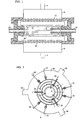
- the Figure is illustrative of an apparatus suitable for growing Si/Ge layers.
- the invention involves the high temperature growth of devices based on Si/Ge alloys.
- a device is a body having a multiplicity of compositionally different regions (besides electrical contact and inactive substrate regions) whose structure is designed to control in a desired manner the transport of charge so as to affect applied energy and/or information.
- Various techniques are available for high temperature growth. For example, MBE or CVD are useful.
- the chemical vapor deposition approach involves equipment and processes which are typically more production-worthy and therefore, for pedagogic reasons, the invention will be described in this context.
- analogous steps provided a high temperature range, i.e., 700 to 1000°C, is employed
- methods such as MBE are also employable.
- the growth of a Si/Ge layer on a substrate is performed below the critical thickness determined from the Matthews-Blakeslee equilibrium curve (see Matthews, supra). If the deposition is confined to satisfy this law, strain will be present in the layer but it will be mechanically stable. Satisfaction of the Matthews/Blakeslee relation depends on the deposition substrate, the composition of the Si/Ge film, and the film thickness. However, suitable parameters defining the substrate and the Si/Ge composition are available in Matthews, supra, for use in the Matthews/Blakeslee determination. For many advantageous devices, such as p-i-n diodes and bipolar transistors, a single crystal silicon substrate is employed. The device region including the Si/Ge composition need not include only this material.
- superlattice devices including alternmating regions of Si/Ge material and silicon with layer thicknesses in the range 20 A to 400 A are useful as the base of a bipolar transistor. Additionally, it is possible to use a region with a graded composition of Si/Ge.
- gaseous materials are introduced to a heated substrate and undergo reaction generally at the substrate.
- gaseous silicon compounds such as dichlorosilane are advantageously employed for the silicon precursor.
- Other silicon gaseous materials are available and useful, but are not as advantageous as dichlorosilane.
- silicon tetrachloride or trichlorosilane decomposes at reasonable rates at a temperature above 950°C and thus for most devices causes excessive dopant diffusion in doped regions present in the deposition substrate.
- silane although decomposing in a suitable temperature regime, induces very fast growth and thus induces control difficulties.
- Germanium tetrachloride is often not available in suitable purity for many devices and is a liquid, thus requiring additional handling associated with introduction as a gas.
- Dopants are also introduced by utilizing a dopant precursor.
- precursors such as arsine or phosphine are used to introduce respectively arsenic and phosphorus doping.
- diborane is advantageously employed as a precursor.
- Flow rates employed depend on the Si/Ge composition desired. Typically, it is convenient to introduce the silicon, germanium, and dopant precursor in a carrier gas. Carrier gases that do not interfere with the desired reaction such as hydrogen, argon, or helium are advantageously used. Dilution levels as low as 1 mole % in the carrier gas for typical flow rates still yield advantageous growth rates. Additionally, at these lower concentrations (1 to 5 mole %), the gases are typically safer to handle.
- the Si/Ge material layer includes from 1 to 60 mole % of germanium. For compositions less than 1 mole %, the bandgap difference is generally insufficient while for compositions of greater than 60 mole % germanium the critical thickness is so thin that formation of the layer is extremely difficult.
- the flow rates employed depend on the composition desired and the degree of dilution in the carrier gas.
- a control sample is easily employed to determine an appropriate flow rate for a desired composition and dilution.
- typical flow rates for 1% dichlorosilane in hydrogen are 0.2 SLPM to 10 SLPM, while flow rates for 1 % germane in hydrogen are advantageously in the range 0.01 SLPM to 0.5 SLPM.
- Lower total flow rates typically produce inconveniently slow growth rate while higher flow rates lead to growth rates sufficiently fast to produce control difficulties.
- Dopant materials are generally diluted to concentrations in the range 1 ppm to 10,000 ppm.
- dopant concentrations in the range 10 16 to 1021 atoms cm 3 are typically employed.
- dopant concentrations of 10 ppm to 10,000 ppm of the dopant in the carrier gas at flow rates in the range 10 sccm to 100 sccm yield dopant concentrations in the range 1016to 10 21 atoms per cm 3 .
- the total pressure is maintained between 1 mTorrand 1 atmosphere. At pressures higher than 1 atmosphere control becomes somewhat difficult while at lower pressures growth rates are inconveniently low.
- the substrate is heated in a cold-wall reactor preferably by utilizing infrared lamps.
- the substrate temperature is determined by using a control sample.
- a substrate is thermally connected to a thermocouple and various voltages are applied to the heating lamps. The temperature response corresponding to a particular voltage calibration is noted and in subsequent use this voltage is used to produce the corresponding temperature.
- Growth is essentially the same whether the precursor gases are present when heating is initiated or whether they are introduced after heating has begun.
- temperatures in the range from 700°C to 1000°C are employed.
- temperatures below 700°C excessive oxygen is incorporated into the layer being grown, while at temperatures above 1000°C excessive germanium and dopant interdiffusion is experienced.
- quartz plates are employed for the reactor walls.
- the gas flow is introduced at 20 symmetrically around the wafer as shown in FIG. 1.
- exhaust is accomplished radially at 30.
- Typical growth rates vary with composition, temperature, and flow rate. However, generally for temperatures of approximately 900°C and Si/Ge compositions with 20% germanium, growth rates of 17 A per second are obtained. This compares favorably with typical growth rates of 0.5 A per second achieved with UHVCVD.
- oxygen contents in the range 2x 10 17 oxygen atoms percm3 are obtainable, three orders of magnitude lower than reported for CVD Si/Ge films deposited at 625°C. (See C.A.
- Si/Ge material is selective on silicon to the essentially complete exclusion of growth on silicon dioxide, for layers up to several micrometers in thickness.
- the deposition substrate was a 10 mm float zone silicon wafer having its major surface in the (100) crystallographic plane and having a resistivity of 100 ohm cm or greater. This substrate was cleaned by sequential immersion in a sulfuric acid/hydrogen peroxide solution (typically 50% sulfuric acid by volume) and in a 1% by volume hydrofluoric acid solution. The substrate, 8, was then placed on the sample holder of a chemical vapor deposition apparatus so that the major surface of the substrate was substantially horizontal.
- a sulfuric acid/hydrogen peroxide solution typically 50% sulfuric acid by volume
- hydrofluoric acid solution typically 50% sulfuric acid by volume
- the chamber was evacuated through conduit 30 (FIG. 2) using a combination of roughing pump and cryopump to a pressure of approximately 10 - 7 Torr.
- a bank of tungsten halogen lamps, 12, cooled by air introduced at 4 were energized and the voltage on these lamps controlled to produce a temperature of the substrate of approximately 300°C.
- the temperature produced was determined earlier by using a calibration substrate having a thermally connected thermocouple and thus, through this calibration, a measured temperature was associated with an applied voltage.
- the lamp housing, 9, was water cooled.
- the baking was continued for approximately 10 minutes.
- a flow of 3 liters per minute of pure hydrogen was then established through inlet 22 resulting in a chamber pressure of about 10 Torr and the voltage of the lamps increased to produce a substrate temperature of 1000°C for 15 seconds.
- the lamps were de-energized, and the wafer was allowed to cool to approximately 200°C. (The cooling took approximately one minute and was predetermined utilizing a calibration substrate with a thermocouple.)
- the deposition substrate reached 200°C the hydrogen flow was terminated and a gas flow of 1000 cc/min of a mixture of dichlorosilane (1% by volume) in hydrogen and 30 cc/min of 10 parts per million (by volume) of arsine in hydrogen was established.
- the wafer again was cooled to 200°C in flowing hydrogen and after cooling the hydrogen gas flow was replaced by a flow through conduit 22 including 890 cc/min of 1% by volume dichlorosilane in hydrogen, 110 cc/min of 1 % by volume germane in hydrogen and 100 cc/min of 1000 ppm by volume of diborane in hydrogen.
- the resulting growth of Si/Ge material was continued for 22 seconds to produce a film thickness of 300 A, a composition of 15 atomic percent Ge in Si, and a p-dopant concentration of 10 19 boron atoms per cubic cm.
- the substrate was again cooled in flowing hydrogen to a temperature of 200°C.
- the hydrogen flow was again replaced by a flow of 1 of cc/min of 1 % dichlorosilane in hydrogen, and 4 cc/min of 1000 ppm by volume of diborane in hydrogen.
- the deposition was continued for approximately 70 seconds to yield a 1000 A thick p-type silicon layer with a 10 16 boron atoms per cm 3 dopant concentration.
- an n-p+-n heterojunction bipolar transistor was fabricated using implantation techniques and conventional processing as des- crided in G.S. Higashi, et al., Applied Physics Letters, 56, 2560 (1990).
- the resulting structure exhibited a base with no relaxation defects and an oxygen concentration of approximately 2x 10 17 oxygen atoms per cm 3 . Even after device processing essentially no relaxation defects were observed by electron microscopy.
- Example 1 The procedure of Example 1 was followed except the growth temperature employed for each of the three layer depositions was 850°C rather than 900°C. Additionally, for growth of the Si/Ge layer the gas flow of dichlorosilane was 900 cc/min and the gas flow of germane was 100 cc/min. The resulting Si/Ge layer was 12 atomic percent germanium and had essentially the same characteristics as that described in Example 1.
- Example 1 The procedure of Example 1 was followed except a transistor was grown on a substrate having both silicon and silicon dioxide regions.
- the substrate as described in Example 1 was selectively oxidized to produce windows larger than or equal to 1 f..lm in a silicon dioxide region overlying the silicon substrate. This silicon dioxide region was formed by thermal oxidation.
- the first transistor layer was formed by the procedure of Example 1 except the dopant utilized was an 80 cc/min flow of 10 ppm arsine.
- the second layer was a region that had a graded concentration of germanium.
- the layer was 250 A thick and varied from 7% germanium at the emitter/base interface to 15 atomic percent germanium at the base/collector interface.
- This grading was accomplished utilizing a total flow of 1000 cc/min of precursor gas, initially employing 110 cc/min of 1 % germanium with the remainder the dichlorosilane, and linearly decreasing the germane flow until it reached 60 cc/min. Doping of this layer was accomplished as described in Example 1.
- the third layer was a 1000 A thick layer of silicon produced utilizing a 55 second deposition from 1000 cc/min flow of 1% dichlorosilane together with a 2 cc/min flow of 1000 ppm diborane. This third layerwas later implanted and the transistor completed as described in Higashi, supra.
- a superlattice was formed on a silicon substrate.
- the silicon substrate was prepared as described in Example 1. Twenty periods were grown on the substrate. Each period included 35 A of a Si/Ge (11 atomic %) composition and 75 A of silicon.
- the Si/Ge composition was grown as described in Example 1 except the growth was for 10 seconds utilizing a 65 cc/min 1 % germane flow and a 935 cc/min dichlorosilane flow. Each silicon region was grown for 10 seconds utilizing a 1000 cc/min dichlorosilane flow.
Landscapes
- Bipolar Transistors (AREA)
- Crystals, And After-Treatments Of Crystals (AREA)
Applications Claiming Priority (2)
| Application Number | Priority Date | Filing Date | Title |
|---|---|---|---|
| US62346690A | 1990-12-07 | 1990-12-07 | |
| US623466 | 1990-12-07 |
Publications (2)
| Publication Number | Publication Date |
|---|---|
| EP0490531A2 true EP0490531A2 (fr) | 1992-06-17 |
| EP0490531A3 EP0490531A3 (en) | 1994-07-13 |
Family
ID=24498181
Family Applications (1)
| Application Number | Title | Priority Date | Filing Date |
|---|---|---|---|
| EP19910311018 Withdrawn EP0490531A3 (en) | 1990-12-07 | 1991-11-28 | Devices based on si/ge |
Country Status (3)
| Country | Link |
|---|---|
| EP (1) | EP0490531A3 (fr) |
| JP (1) | JPH04268722A (fr) |
| CA (1) | CA2050649A1 (fr) |
Family Cites Families (4)
| Publication number | Priority date | Publication date | Assignee | Title |
|---|---|---|---|---|
| JPS5710920A (en) * | 1980-06-23 | 1982-01-20 | Canon Inc | Film forming process |
| US4442449A (en) * | 1981-03-16 | 1984-04-10 | Fairchild Camera And Instrument Corp. | Binary germanium-silicon interconnect and electrode structure for integrated circuits |
| JPS63285923A (ja) * | 1987-05-19 | 1988-11-22 | Komatsu Denshi Kinzoku Kk | シリコン−ゲルマニウム合金の製造方法 |
| US4910163A (en) * | 1988-06-09 | 1990-03-20 | University Of Connecticut | Method for low temperature growth of silicon epitaxial layers using chemical vapor deposition system |
-
1991
- 1991-09-04 CA CA002050649A patent/CA2050649A1/fr not_active Abandoned
- 1991-11-28 EP EP19910311018 patent/EP0490531A3/en not_active Withdrawn
- 1991-12-05 JP JP3320834A patent/JPH04268722A/ja not_active Withdrawn
Also Published As
| Publication number | Publication date |
|---|---|
| EP0490531A3 (en) | 1994-07-13 |
| CA2050649A1 (fr) | 1992-06-08 |
| JPH04268722A (ja) | 1992-09-24 |
Similar Documents
| Publication | Publication Date | Title |
|---|---|---|
| US4912063A (en) | Growth of beta-sic thin films and semiconductor devices fabricated thereon | |
| US5120394A (en) | Epitaxial growth process and growing apparatus | |
| US4912064A (en) | Homoepitaxial growth of alpha-SiC thin films and semiconductor devices fabricated thereon | |
| US4767494A (en) | Preparation process of compound semiconductor | |
| US4808551A (en) | Method for halide VPE of III-V compound semiconductors | |
| JP4417625B2 (ja) | トリシランを用いる混合基板への成膜方法、および、ベース構造の製造方法 | |
| EP0518800B1 (fr) | Croissance hétéroépitaxiale de germanium sur silicium par CVD sous vide très poussée | |
| US20040219735A1 (en) | Epitaxial semiconductor deposition methods and structures | |
| US5296258A (en) | Method of forming silicon carbide | |
| EP0681315B1 (fr) | Procédé de formation sélective de régions semi-conductrices | |
| TWI893031B (zh) | 磊晶晶圓之製造方法 | |
| Hsieh et al. | Silicon homoepitaxy by rapid thermal processing chemical vapor deposition (RTPCVD)—A review | |
| JPS6329928A (ja) | シリコン上にガリウムヒ素をエピタキシヤル成長せしめる方法 | |
| US5387545A (en) | Impurity diffusion method | |
| US3669769A (en) | Method for minimizing autodoping in epitaxial deposition | |
| Hirayama et al. | High doping of phosphorus in Si using gas source molecular beam epitaxy | |
| EP0241204B1 (fr) | Méthode pour former une couche cristalline déposée | |
| US3765960A (en) | Method for minimizing autodoping in epitaxial deposition | |
| US5286334A (en) | Nonselective germanium deposition by UHV/CVD | |
| JP3214505B2 (ja) | 半導体装置の製造方法 | |
| EP0490531A2 (fr) | Dispositifs semi-conducteurs avec alliages à base de Si/Ge | |
| JP3322740B2 (ja) | 半導体基板およびその製造方法 | |
| Jang et al. | Growth of epitaxial Si1-xGex layers at 750° C by VLPCVD | |
| WO2004084268A2 (fr) | Procedes de depot epitaxial de semiconducteur et structures correspondantes | |
| Green et al. | High gain Si Ge heterojunction bipolar transistors grown by rapid thermal chemical vapor deposition |
Legal Events
| Date | Code | Title | Description |
|---|---|---|---|
| PUAI | Public reference made under article 153(3) epc to a published international application that has entered the european phase |
Free format text: ORIGINAL CODE: 0009012 |
|
| AK | Designated contracting states |
Kind code of ref document: A2 Designated state(s): DE FR GB |
|
| PUAL | Search report despatched |
Free format text: ORIGINAL CODE: 0009013 |
|
| RAP3 | Party data changed (applicant data changed or rights of an application transferred) |
Owner name: AT&T CORP. |
|
| AK | Designated contracting states |
Kind code of ref document: A3 Designated state(s): DE FR GB |
|
| 17P | Request for examination filed |
Effective date: 19941208 |
|
| 17Q | First examination report despatched |
Effective date: 19950518 |
|
| STAA | Information on the status of an ep patent application or granted ep patent |
Free format text: STATUS: THE APPLICATION IS DEEMED TO BE WITHDRAWN |
|
| 18D | Application deemed to be withdrawn |
Effective date: 19960910 |