EP0490923B1 - Reseau de diffraction et procede de fabrication correspondant - Google Patents
Reseau de diffraction et procede de fabrication correspondant Download PDFInfo
- Publication number
- EP0490923B1 EP0490923B1 EP90912877A EP90912877A EP0490923B1 EP 0490923 B1 EP0490923 B1 EP 0490923B1 EP 90912877 A EP90912877 A EP 90912877A EP 90912877 A EP90912877 A EP 90912877A EP 0490923 B1 EP0490923 B1 EP 0490923B1
- Authority
- EP
- European Patent Office
- Prior art keywords
- grating
- diffraction grating
- image
- further characterised
- pixels
- Prior art date
- Legal status (The legal status is an assumption and is not a legal conclusion. Google has not performed a legal analysis and makes no representation as to the accuracy of the status listed.)
- Expired - Lifetime
Links
Images


Classifications
-
- B—PERFORMING OPERATIONS; TRANSPORTING
- B42—BOOKBINDING; ALBUMS; FILES; SPECIAL PRINTED MATTER
- B42D—BOOKS; BOOK COVERS; LOOSE LEAVES; PRINTED MATTER CHARACTERISED BY IDENTIFICATION OR SECURITY FEATURES; PRINTED MATTER OF SPECIAL FORMAT OR STYLE NOT OTHERWISE PROVIDED FOR; DEVICES FOR USE THEREWITH AND NOT OTHERWISE PROVIDED FOR; MOVABLE-STRIP WRITING OR READING APPARATUS
- B42D25/00—Information-bearing cards or sheet-like structures characterised by identification or security features; Manufacture thereof
- B42D25/30—Identification or security features, e.g. for preventing forgery
- B42D25/342—Moiré effects
-
- B—PERFORMING OPERATIONS; TRANSPORTING
- B42—BOOKBINDING; ALBUMS; FILES; SPECIAL PRINTED MATTER
- B42D—BOOKS; BOOK COVERS; LOOSE LEAVES; PRINTED MATTER CHARACTERISED BY IDENTIFICATION OR SECURITY FEATURES; PRINTED MATTER OF SPECIAL FORMAT OR STYLE NOT OTHERWISE PROVIDED FOR; DEVICES FOR USE THEREWITH AND NOT OTHERWISE PROVIDED FOR; MOVABLE-STRIP WRITING OR READING APPARATUS
- B42D25/00—Information-bearing cards or sheet-like structures characterised by identification or security features; Manufacture thereof
- B42D25/30—Identification or security features, e.g. for preventing forgery
- B42D25/309—Photographs
-
- B—PERFORMING OPERATIONS; TRANSPORTING
- B42—BOOKBINDING; ALBUMS; FILES; SPECIAL PRINTED MATTER
- B42D—BOOKS; BOOK COVERS; LOOSE LEAVES; PRINTED MATTER CHARACTERISED BY IDENTIFICATION OR SECURITY FEATURES; PRINTED MATTER OF SPECIAL FORMAT OR STYLE NOT OTHERWISE PROVIDED FOR; DEVICES FOR USE THEREWITH AND NOT OTHERWISE PROVIDED FOR; MOVABLE-STRIP WRITING OR READING APPARATUS
- B42D25/00—Information-bearing cards or sheet-like structures characterised by identification or security features; Manufacture thereof
- B42D25/30—Identification or security features, e.g. for preventing forgery
- B42D25/324—Reliefs
-
- B—PERFORMING OPERATIONS; TRANSPORTING
- B42—BOOKBINDING; ALBUMS; FILES; SPECIAL PRINTED MATTER
- B42D—BOOKS; BOOK COVERS; LOOSE LEAVES; PRINTED MATTER CHARACTERISED BY IDENTIFICATION OR SECURITY FEATURES; PRINTED MATTER OF SPECIAL FORMAT OR STYLE NOT OTHERWISE PROVIDED FOR; DEVICES FOR USE THEREWITH AND NOT OTHERWISE PROVIDED FOR; MOVABLE-STRIP WRITING OR READING APPARATUS
- B42D25/00—Information-bearing cards or sheet-like structures characterised by identification or security features; Manufacture thereof
- B42D25/40—Manufacture
- B42D25/405—Marking
- B42D25/41—Marking using electromagnetic radiation
-
- B—PERFORMING OPERATIONS; TRANSPORTING
- B42—BOOKBINDING; ALBUMS; FILES; SPECIAL PRINTED MATTER
- B42D—BOOKS; BOOK COVERS; LOOSE LEAVES; PRINTED MATTER CHARACTERISED BY IDENTIFICATION OR SECURITY FEATURES; PRINTED MATTER OF SPECIAL FORMAT OR STYLE NOT OTHERWISE PROVIDED FOR; DEVICES FOR USE THEREWITH AND NOT OTHERWISE PROVIDED FOR; MOVABLE-STRIP WRITING OR READING APPARATUS
- B42D25/00—Information-bearing cards or sheet-like structures characterised by identification or security features; Manufacture thereof
- B42D25/40—Manufacture
- B42D25/405—Marking
- B42D25/425—Marking by deformation, e.g. embossing
-
- G—PHYSICS
- G02—OPTICS
- G02B—OPTICAL ELEMENTS, SYSTEMS OR APPARATUS
- G02B5/00—Optical elements other than lenses
- G02B5/18—Diffraction gratings
- G02B5/1842—Gratings for image generation
-
- G—PHYSICS
- G03—PHOTOGRAPHY; CINEMATOGRAPHY; ANALOGOUS TECHNIQUES USING WAVES OTHER THAN OPTICAL WAVES; ELECTROGRAPHY; HOLOGRAPHY
- G03H—HOLOGRAPHIC PROCESSES OR APPARATUS
- G03H1/00—Holographic processes or apparatus using light, infrared or ultraviolet waves for obtaining holograms or for obtaining an image from them; Details peculiar thereto
- G03H1/26—Processes or apparatus specially adapted to produce multiple sub- holograms or to obtain images from them, e.g. multicolour technique
- G03H1/30—Processes or apparatus specially adapted to produce multiple sub- holograms or to obtain images from them, e.g. multicolour technique discrete holograms only
-
- G—PHYSICS
- G06—COMPUTING OR CALCULATING; COUNTING
- G06K—GRAPHICAL DATA READING; PRESENTATION OF DATA; RECORD CARRIERS; HANDLING RECORD CARRIERS
- G06K19/00—Record carriers for use with machines and with at least a part designed to carry digital markings
- G06K19/06—Record carriers for use with machines and with at least a part designed to carry digital markings characterised by the kind of the digital marking, e.g. shape, nature, code
- G06K19/08—Record carriers for use with machines and with at least a part designed to carry digital markings characterised by the kind of the digital marking, e.g. shape, nature, code using markings of different kinds or more than one marking of the same kind in the same record carrier, e.g. one marking being sensed by optical and the other by magnetic means
- G06K19/10—Record carriers for use with machines and with at least a part designed to carry digital markings characterised by the kind of the digital marking, e.g. shape, nature, code using markings of different kinds or more than one marking of the same kind in the same record carrier, e.g. one marking being sensed by optical and the other by magnetic means at least one kind of marking being used for authentication, e.g. of credit or identity cards
- G06K19/16—Record carriers for use with machines and with at least a part designed to carry digital markings characterised by the kind of the digital marking, e.g. shape, nature, code using markings of different kinds or more than one marking of the same kind in the same record carrier, e.g. one marking being sensed by optical and the other by magnetic means at least one kind of marking being used for authentication, e.g. of credit or identity cards the marking being a hologram or diffraction grating
-
- B—PERFORMING OPERATIONS; TRANSPORTING
- B42—BOOKBINDING; ALBUMS; FILES; SPECIAL PRINTED MATTER
- B42D—BOOKS; BOOK COVERS; LOOSE LEAVES; PRINTED MATTER CHARACTERISED BY IDENTIFICATION OR SECURITY FEATURES; PRINTED MATTER OF SPECIAL FORMAT OR STYLE NOT OTHERWISE PROVIDED FOR; DEVICES FOR USE THEREWITH AND NOT OTHERWISE PROVIDED FOR; MOVABLE-STRIP WRITING OR READING APPARATUS
- B42D25/00—Information-bearing cards or sheet-like structures characterised by identification or security features; Manufacture thereof
- B42D25/30—Identification or security features, e.g. for preventing forgery
- B42D25/328—Diffraction gratings; Holograms
Definitions
- This invention relates to diffraction gratings and to their manufacture and in particular provides diffraction gratings which may be adapted for application as security devices, for example, in currency notes and credit cards.
- the 1988 plastic Australian ten-dollar note employs as an anti-counterfeiting security device, a diffraction grating image of Captain Cook which comprises a regular matrix of pixels each containing a curvilinear segment of one or more of the grating lines. These pixels when illuminated each generate a two-dimensional optical catastrophe image diffraction pattern whereby the total image diffraction pattern of the grating is optically variable but structurally stable.
- the Captain Cook image is an application of the present inventor's theory of generalised curvilinear diffraction gratings to optical diffraction catastrophes. The theory is outlined in Optica Acta, 1983, Vol. 30 Nos. 3 and 4, and the application to optical diffraction catastrophes is disclosed in Vol. 30, No. 4, 449 - 464. In essence, the Captain Cook image entails the imposition of a matrix of diffraction catastrophe pixels on a regular diffraction grating.
- image diffraction pattern in the context of this specification is meant the optical image observed by the naked eye focused on the grating when it is illuminated by an arbitrarily extended diffuse source of finite width such as a fluorescent tube.
- diffraction grating indicates a grating of either reflective or transmissive lines.
- a pattern is described herein as “optically variable” where it varies according to the position of observation and is “structurally stable” if its broad form at any given position of observation is not materially altered by slight distortions of the grating surface.
- the Captain cook pixellated diffraction grating image is substantially more secure that the traditional metal foil insert and is an improvement over security devices such as multiple film devices, conventional straight line grating and image holograms because, in contrast to these devices, it is able to sustain an acceptable level of structural stability as the notes become heavily crinkled in day-to-day use.
- security devices such as multiple film devices, conventional straight line grating and image holograms because, in contrast to these devices, it is able to sustain an acceptable level of structural stability as the notes become heavily crinkled in day-to-day use.
- EP-A-375833 an application filed before but published after the filing date of this application, also discloses a pixellated diffraction grating device in which an optically invariable image is divided into multiple pixels.
- the invention in its first aspect, relates to the concept of producing an individual corresponding diffraction grating pixel for successive pixels of the optically invariable image, and, in a preferred arrangement, arranging for the grating pixels to reflect that observed chroma or colour value of the image pixels.
- the invention involves the realisation that a reproduction of a diffraction grating by reflection contact printing will be flawed by moire or Talbot fringe effects, and that the pixellated diffraction grating can be designed to amplify the visual impact of these Talbot fringes to an extent that very obviously flaws a counterfeit reproduction of the grating.
- the moire or Talbot fringes are a function of the inevitable spacing between the photographic plate and the grating, and of variations of the local groove spacing across the grating plane.
- the invention accordingly provides, in a first aspect a method of forming a diffraction grating which provides an optically variable image, said image being optically variable in that it varies according to the position of observation, comprising:
- each grating pixel is also a function of the assessed chroma or colour value of the associated pixel in said optically invariable image so that the pixellated diffraction grating when illuminated generates a visually recognisable but optically variable reproduction of said optically invariable image. Still more advantageously, each grating pixel is such that the pixellated diffraction grating is also structurally stable reproduction of said optically invariable image.
- optical diffraction grating is meant a grating which when illuminated will generate a two dimensional optical image diffraction pattern.
- the invention extends to a diffraction grating device providing an optically variable image corresponding to an optically invariable counterpart image, comprising a pixellated diffraction grating which is an assembly of diffraction grating pixels and which when illuminated generates an optically variable image, said image being optically variable in that it varies according to the position of observation, wherein each of said diffraction grating pixels is an individual optical catastrophe diffraction grating, and wherein said diffraction grating pixels comprise respective sets of reflective or transmissive lines having a curvature which varies between pixels and which is related to a predetermined greyness factor of an associated pixel of the optically invariable counterpart image of said optically variable image.
- the chroma or colour value may be a greyness factor on a scale, e.g. of 1 to 7 or 1 to 16.
- a diffraction grating formed by a regular matrix of pixels which when illuminated each generate a two-dimensional optical image diffraction pattern, wherein the grating in some or all of the pixels is arranged such that a reproduction of said grating by reflection contact printing generates a zero order pattern which is grossly flawed by moire or Talbot fringe effects, preferably to the extent that the zero order pattern of the reproduction is a cross between a negative and a positive of the zero order pattern of the original grating.
- the Hessian of C ij (x,y) is a standard complex derivative expressed as follows: ⁇ 2 C ij (x,y)/ ⁇ x 2 . ⁇ 2 C ij (x,y)/ ⁇ y 2 -[ ⁇ 2 C ij (x,y)/ ⁇ x ⁇ y] 2
- each grating pixel may be an individual optical catastrophe diffraction grating of the associated pixel in said optically invariable image. This occurs for (1) above when the Hessian is not identically zero except along certain characteristic lines corresponding to the caustics in the Fresnel or Fraunhofer diffraction pattern of the grating.
- a particularly effective set of functions suitable to be C ij (x,y) are those comprising products or sums of sinusoidal terms, or a combination thereof.
- favoured functions are those which are easily scalable to chroma or colour value, are smooth, and are easily programmed.
- the right side of equation (1) may include a further summed term Sd(x,y), being a shield function of periodicity substantially greater than the pixel dimensions.
- This shield function may be a further sum and/or product of sinusoidal terms of greater periodicity than C ij (x,y).
- the second aspect of the invention may be practised by the inclusion of different periodicity terms in the sinusoidal components of C ij (x,y).
- the moire or Talbot fringe effects in a reproduction will be amplified by selecting function terms which will generate highly curved wave fronts.
- the pixels are preferably less than 1mm 2 in area most preferably squares.
- the reflective/transmissive lines are advantageously reflective grooves, e.g. square cut grooves, in a metallised surface.
- the invention extends of course to the combination of the two aspects of the invention in the one grating image.
- each pixel is an individual optical diffraction grating of the associated pixel in the original image and also a function of the assessed grey level of that associated pixel of the original image. It will be understood that each pixel of the original image is mapped to a respective pixel of the pixellated grating.
- Figure 2 is the diffraction image at a given viewing angle generated when the pixellated grating is illuminated.
- This image consists of 166 x 208 pixels, each 0.125 mm square.
- the actual grating size is 20.75mm x 26mm and there 14 grey levels in the assessment scale.
- the pattern is a visually recognisable but optically variable reproduction of the original optically invariable image of Figure 1.
- This form of grating function embodies both aspects of the invention.
- the product of two sinusoidal terms of different periodicity is effective to generate gross flaw moire or Talbot fringe in a reflection contact printing reproduction of the grating image.
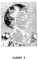
- Such a reproduction pixellated grating for Figure 1 generates the zero-order image diffraction pattern shown in Figure 3: it is visually substantially a cross between a negative and a positive of the image diffraction pattern of the original grating and is very obviously flawed to any observer.
- the copy plate separation was 10 microns and the exposure was equivalent to 5 Talbot fringes.
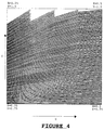
- FIG. 4 A magnified view of an exemplary pixel grating is shown in Figure 4.
- This is actually a computer plot of one of the pixel gratings produced from Figure 1 and the optical effect arising from slight discontinuities in the lines is a printer artefact.
- the lines are shallow parabolas.
- the effect of decreasing grey level parameter ⁇ is to spread the lines apart, more at the centre than at the edges, thereby increasing the curvature of each parabola.
- This of course has the effect of lightening the grey level of the pixel in the grating image diffraction pattern so that the overall effect is that the grating image diffraction pattern is a pixellated visually recognisable reproduction of the original image.
- the pixel of Figure 4 is for the lightest of the 14 shades of grey i.e.
- each curved grating line or groove is approximated by 4 straight line segments at different angles and connected end to end.
- Each straight line segment is in reality a miniature polygon in the shape of a rhombus with a well defined width as shown in the enlargement of Figure 5A.
- Figure 5B is an extreme close-up of a section of a typical pixel showing the butting together of polygon groove segments and variations in groove width.
- Figure 6 depicts a small group of 10 x 10 pixels from the central region of the grating of Figure 2, showing differences in groove curvature from pixel to pixel for clarity only a few grooves have been plotted in each pixel.
- S ij (x,y) may be adjusted to select the brightness and stability of each pixel, choose the colour and orientation of each pixel, fix the distance and angle at which the diffracted image has maximum clarity and finally to choose the light sources that give maximum effect to the diffracted portrait image.
- the grating lines are grooves
- the groove depths should be optimised for maximum diffraction efficiency. For a square wave groove profile this generally means that the groove depth should be about 40 per cent of the average groove spacing. In the case of the grating of Figure 4, the groove depth should be about 0.5 to 0.6 micron, most preferably about 0.56 micron.
- An actual grating of the form of Figure 2 has been constructed by programming an electron beam lithography system.
- the grating was written on PMMA electron resist spin coated onto a chrome coated glass substrate, which may be then processed to produce a gold coated nickel master from which plastic film replica gratings are pressed.
- the practical process effectively entails converting any given photograph of a portrait or scene into a set of data files that are used to control the exposure and writing characteristics of the electron beam lithography system in such a way as to enable the machine to produce corresponding master gratings according to the invention.
- the portrait is scanned into a computer graphics system via a high quality colour scanner such as a Sharp JX-300 and then processed by a special purpose interactive software package built around the inventor's aforementioned theory of generalised diffraction gratings.
- This software package provides the grating designer with a set of options for converting the portrait data into a diffraction line pattern and corresponding data file for electron beam fabrication of the grating by the electron beam lithography system.
- the first part of the program "screens" the digitised portrait into the selected array of N X M pixels.
- the resolution of the screen or pixel size is the choice of the designer and obviously the smaller the pixels, the larger the resultant data file.
- the second part of the program converts each pixel of the screened portrait into its corresponding diffraction grating as discussed above.
- the final part of the design program consists of a set of subroutines for displaying the observed diffraction patterns of the grating under a range of light sources and observing conditions. If an initial design is not satisfactory in some respect, the designer can then go back and modify the design before producing the final data file for electron beam fabrication of the grating.
- a durable metal master of the optimised grating may be obtained by vacuum coating the photoresist master with 200 Angstroms of 99.99% gold and electro-depositing a thick layer of nickel to act as a support.
- this gold coated nickel master may be bonded to a brass block and used as a die for hot pressing of plastic film replica gratings.
- the temperature and pressure combinations associated with the hot embossing process should be such that the replicated groove depths are as close as possible to the original 0.56 micron groove depth of the metal die.
- the plastic replicas may be adhesively attached to currency notes or credit cards.
- the present invention it is possible to produce diffraction gratings which generate realistic text and portrait images of near photographic quality.
- the images may be both sharply defined and optically variable under most lighting conditions including very diffuse sources. This is in contrast to the case of the holograms which produce very fuzzy images and lose their optical variability under overcast lighting conditions.
- the kinegram optically variable device used on the Austrian 5,000 schilling banknote retains a high degree of optically variability under diffuse lighting conditions, but only produces schematic types of images.
- the optical variability of the invention is also easily defined; the image simply changes from positive to negative as the angle of observation changes.
- the images generated by the invention also exhibit a high degree of structural stability with respect to bending undulations of the grating surface. They are therefore suitable security devices for currency notes and share certificates etc.
- a grating according to the preferred embodiment is observed directly under an extended source such as a fluorescent tube the intensities of the pixels varying smoothly with changing angle of view.
- the pixels may be said to possess a degree of structural stability because any perturbation of the initial wavefront due to crinkling of the grating surface in the vicinity of the pixel will only cause a change of intensity in the pixel.
- Preferred gratings of the type described here are designed, in accordance with the second aspect of the invention, to be resistant to copying by the well known method of reflection contact printing.
- the zero order portrait image of the copy grating becomes covered in amass of dark spoiler bands thereby making the zero order portrait image unrecognisable.
- holograms and kinegrams are easily counterfeited by this method.
- An additional related feature of the invention is the ability to selectively vary the groove depth of the pixels by varying the electron beam current during the grating fabrication process in such away as to cause a visible text or graphic image to appear in the zero diffraction order.
- This additional static image does not appear with any clarity on a reflection contact print counterfeit of the grating and is therefore an added security feature.
- these diffraction gratings are binary phase devices and are therefore easily mass produced by the same embossing method used for holograms.
- An alternative approach to the second aspect of the invention is to use a C ij (x,y) with sinusoidal terms of similar periodicity and to impose a summed shield function Sd(x,y) of longer periodicity extending over several pixels.
Landscapes
- Physics & Mathematics (AREA)
- Engineering & Computer Science (AREA)
- General Physics & Mathematics (AREA)
- Manufacturing & Machinery (AREA)
- Toxicology (AREA)
- General Health & Medical Sciences (AREA)
- Electromagnetism (AREA)
- Health & Medical Sciences (AREA)
- Optics & Photonics (AREA)
- Theoretical Computer Science (AREA)
- Diffracting Gratings Or Hologram Optical Elements (AREA)
- Crystals, And After-Treatments Of Crystals (AREA)
- Optical Filters (AREA)
Claims (42)
- Procédé de formation d'un réseau de diffraction qui produit une image optiquement variable, ladite image étant optiquement variable en ce sens qu'elle varie selon la position d'observation, procédé comprenant les étapes consistant à :diviser une image optiquement invariable en de multiples pixels;déterminer un pixel à réseau de diffraction correspondant pour chacun desdits pixels de l'image optiquement invariable, lequel pixel à réseau de diffraction est un réseau de diffraction individuel à catastrophe optique correspondant à un pixel correspondant de l'image optiquement invariable; etproduire un réseau de diffraction pixélisé qui comprend un ensemble desdits pixels à réseau de diffraction et qui, lorsqu'il est éclairé, génère une reproduction optiquement variable de ladite image optiquement invariable,dans lequel un facteur de gris est déterminé pour chacun desdits pixels de l'image optiquement invariable et lesdits pixels à réseau de diffraction comprennent des groupes respectifs de lignes réfléchissantes ou transparentes ayant une courbure qui varie d'un pixel à l'autre et qui est liée au facteur de gris déterminé du pixel correspondant de l'image optiquement invariable.
- Procédé selon la revendication 1, caractérisé en outre en ce que chaque pixel à réseau est tel que le réseau de diffraction pixélisé est aussi une reproduction structurellement stable de ladite image optiquement invariable en ce sens que sa forme large à n'importe quelle position d'observation donnée n'est pas matériellement modifiée par de légères distorsions de la surface du réseau.
- Procédé selon la revendication 1 ou 2, dans lequel la courbure dudit groupe de lignes réfléchissantes ou transparentes d'un pixel à réseau de diffraction est inversement proportionnelle au facteur de gris.
- Procédé selon l'une quelconque des revendications précédentes, caractérisé en outre en ce que chaque réseau individuel de diffraction optique comprend des lignes réfléchissantes ou transparentes définies, en termes de coordonnées x,y dans le plan du réseau, par l'équation S(x,y) = kN où k est un facteur d'échelle, N est un entier et la fonction S(x,y) est donnée par :Sij(x,y) est la fonction de phase initiale générée par le pixel à réseau ij quand il est éclairé normalement par une onde lumineuse monochromatique collimatée,Wij(x,y) est une onde porteuse d'ordre non zéro,Cij(x,y) est une fonction de x,y qui varie rapidement par rapport à x et y et dont le Hessien n'est pas identiquement zéro, c'est-à-dire ne s'évanouit pas identiquement;βij est un facteur proportionnel à la valeur évaluée de chrominance ou de couleur; eti,j sont les coordonnées des pixels respectifs.
- Procédé selon la revendication 4, caractérisé en outre en ce que la fonction Cij(x,y) est choisie parmi le groupe de fonctions comprenant des produits ou des sommes de termes sinusoïdaux, ou une combinaison de ceux-ci.
- Procédé selon l'une quelconque des revendications précédentes, caractérisé en outre en ce que la fonction de réseau de certains ou de l'ensemble des pixels est sélectionnée de façon qu'une reproduction dudit réseau de diffraction pixélisé par tirage contact réfléchissant génère un motif d'ordre zéro qui est grossièrement dégradé par des effets de moiré ou de franges de Talbot.
- Procédé selon la revendication 6, caractérisé en outre en ce que ladite fonction de réseau comprend des termes sinusoïdaux de périodicité différente de façon que le motif d'ordre zéro de la reproduction est un croisement entre un négatif et un positif du motif d'ordre zéro du réseau original à partir duquel la reproduction est réalisée.
- Procédé selon la revendication 6 ou 7 lorsqu'elle dépend de la revendication 5, caractérisé en outre en ce que les composantes sinusoïdales de Cij(x,y) comprennent des termes de périodicité différente de façon à générer des fronts d'onde très incurvés.
- Procédé selon la revendication 6 ou 7 lorsqu'elle dépend de la revendication 5, caractérisé en outre en ce que le membre droit de l'équation (1) comprend un autre terme additionné de fonction d'écran d'une périodicité sensiblement supérieure aux dimensions des pixels.
- Procédé selon la revendication 9, caractérisé en outre en ce que ledit autre terme additionné est une somme et/ou un produit de termes sinusoïdaux de périodicité supérieure à Cij(x,y).
- Procédé selon l'une quelconque des revendications précédentes, caractérisé en outre en ce que les pixels à réseau sont des carrés de moins de 1 mm2 de surface.
- Procédé selon l'une quelconque des revendications précédentes, caractérisé en outre en ce que le réseau de diffraction pixélisé est produit en formant des sillons réfléchissants, par exemple des sillons carrés, dans une surface métallisée.
- Procédé selon l'une quelconque des revendications précédentes, caractérisé en outre en ce que ledit réseau de diffraction pixélisé est un réseau original durable formé par lithographie par faisceau électronique, à partir duquel de multiples répliques de réseau peuvent être produites.
- Procédé selon la revendication 9, caractérisé en outre en ce que ledit terme de fonction d'écran est composé d'une somme et/ou d'un produit de fonctions sinusoïdales afin d'amener le réseau de diffraction à diffracter des fronts d'onde très incurvés qui amplifient lesdits effets de franges de Talbot générés lors d'un tirage contact réfléchissant du réseau.
- Procédé selon l'une quelconque des revendications précédentes, caractérisé en outre en ce qu'une image optiquement variable observable lorsque le réseau est éclairé varie d'une image positive à l'image négative inverse correspondante lorsque l'angle d'observation change.
- Procédé selon l'une quelconque des revendications précédentes, caractérisé en outre en ce que lesdites lignes réfléchissantes ou transparentes sont formées comme des sillons et caractérisé en outre par une variation sélective de la profondeur des sillons des pixels à réseau de façon à faire apparaítre une image visible d'un texte ou d'un graphique dans l'ordre zéro de diffraction.
- Procédé selon la revendication 16 lorsqu'elle dépend de la revendication 13, caractérisé en outre en ce qu'on fait varier ladite profondeur des sillons en faisant varier le courant du faisceau électronique dans ladite lithographie par faisceau électronique.
- Procédé selon l'une quelconque des revendications précédentes, caractérisé en outre en ce que lesdits facteurs de gris des pixels de l'image optiquement invariable sont sélectionnés parmi une échelle contenant un nombre fini et prédéterminé de valeurs de facteur de gris.
- Procédé selon l'une quelconque des revendications précédentes, caractérisé en outre par la production dudit réseau de diffraction pixélisé en réplique de réseau par pressage à chaud avec un moule comprenant un réseau original.
- Procédé selon la revendication 13 ou 19, caractérisé en outre en ce que le réseau original est un original en nickel plaqué d'or.
- Procédé selon l'une quelconque des revendications précédentes, caractérisé en outre par la formation desdites lignes réfléchissantes ou transparentes sous forme de segments de sillons polygonaux de profondeur, de largeur et d'espacement variables.
- Procédé selon la revendication 21, caractérisé en outre par l'ajustement desdites fonctions pour sélectionner la brillance, la stabilité et la couleur des pixels.
- Dispositif à réseau de diffraction produisant une image optiquement variable correspondant à une image équivalente optiquement invariable, comprenant un réseau de diffraction pixélisé qui est un ensemble de pixels à réseau de diffraction et qui, lorsqu'il est éclairé, génère une image optiquement variable, ladite image étant optiquement variable en ce sens qu'elle varie selon la position d'observation, dans lequel chacun desdits pixels à réseau de diffraction est un réseau de diffraction individuel à catastrophe optique et dans lequel lesdits pixels à réseau de diffraction comprennent des groupes respectifs de lignes réfléchissantes ou transparentes ayant une courbure qui varie d'un pixel à l'autre et qui est liée à un facteur de gris prédéterminé d'un pixel correspondant de l'image équivalente optiquement invariable de ladite image optiquement variable.
- Réseau de diffraction selon la revendication 23, caractérisé en outre en ce que chaque pixel à réseau varie aussi en fonction d'une valeur de chrominance ou de couleur.
- Réseau de diffraction selon la revendication 23 ou 24, caractérisé en outre en ce que chaque pixel à réseau est tel que le réseau de diffraction pixélisé est aussi une image structurellement stable en ce sens que sa forme large à n'importe quelle position d'observation donnée n'est pas matériellement modifiée par de légères distorsions de la surface du réseau.
- Réseau de diffraction selon l'une quelconque des revendications 23 à 25, caractérisé en outre en ce que lesdites lignes ont une densité de lignes qui varie d'un pixel à l'autre et qui est liée à une valeur prédéterminée de chrominance ou de couleur du pixel correspondant de l'image optiquement invariable.
- Réseau de diffraction selon l'une quelconque des revendications 23 à 26, dans lequel la courbure dudit groupe de lignes réfléchissantes ou transparentes d'un pixel à réseau de diffraction est inversement proportionnelle au facteur de gris.
- Réseau de diffraction selon l'une quelconque des revendications 23 à 27, caractérisé en outre en ce que chaque réseau individuel de diffraction optique comprend des lignes réfléchissantes ou transparentes définies, en termes de coordonnées x,y dans le plan du réseau, par l'équation S(x,y) = kN où k est un facteur d'échelle, N est un entier et la fonction S(x,y) est donnée par :Sij(x,y) est la fonction de phase initiale générée par le pixel à réseau ij quand il est éclairé normalement par une onde lumineuse monochromatique collimatée,Wij(x,y) est une onde porteuse d'ordre non zéro,Cij(x,y) est une fonction de x,y qui varie rapidement par rapport à x et y et dont le Hessien n'est pas identiquement zéro, c'est-à-dire ne s'évanouit pas identiquement;βij est un facteur proportionnel à la valeur évaluée de chrominance ou de couleur; eti,j sont les coordonnées des pixels respectifs.
- Réseau de diffraction selon la revendication 28, caractérisé en outre en ce que la fonction Cij(x,y) est choisie parmi le groupe de fonctions comprenant des produits ou des sommes de termes sinusoïdaux, ou une combinaison de ceux-ci.
- Réseau de diffraction selon l'une quelconque des revendications 23 à 29, caractérisé en outre en ce que la fonction de réseau de certains ou de l'ensemble des pixels est sélectionnée de façon qu'une reproduction dudit réseau de diffraction pixélisé par tirage contact réfléchissant génère un motif d'ordre zéro qui est grossièrement dégradé par des effets de moiré ou de franges de Talbot.
- Réseau de diffraction selon la revendication 30, caractérisé en outre en ce que ladite fonction de réseau comprend des termes sinusoïdaux de périodicité différente de façon que le motif d'ordre zéro de la reproduction est un croisement entre un négatif et un positif du motif d'ordre zéro du réseau original à partir duquel la reproduction a été réalisée.
- Réseau de diffraction selon la revendication 30 ou 31 lorsqu'elle dépend de la revendication 29, caractérisé en outre en ce que les composantes sinusoïdales de Cij(x,y) comprennent des termes de périodicité différente de façon à générer des fronts d'onde très incurvés.
- Réseau de diffraction selon la revendication 31 ou 32 lorsqu'elle dépend de la revendication 28, caractérisé en outre en ce que le membre droit de l'équation (1) comprend un autre terme additionné de fonction d'écran d'une périodicité sensiblement supérieure aux dimensions des pixels.
- Réseau de diffraction selon l'une quelconque des revendications 23 à 33, caractérisé en outre en ce que les pixels à réseau sont des carrés de moins de 1 mm2 de surface.
- Réseau de diffraction selon l'une quelconque des revendications 23 à 34, caractérisé en outre en ce que ledit réseau pixélisé comprend des lignes réfléchissantes ou transparentes d'une profondeur qui varie de façon à faire apparaítre une image visible statique d'un texte ou d'un graphique dans l'ordre zéro de diffraction.
- Réseau de diffraction selon l'une quelconque des revendications 23 à 35, comprenant un réseau original durable formé par lithographie par faisceau électronique, à partir duquel de multiples répliques de réseau peuvent être produites.
- Réseau de diffraction selon la revendication 33, caractérisé en outre en ce que ledit terme de fonction d'écran est composé d'une somme et/ou d'un produit de fonctions sinusoïdales afin d'amener le réseau de diffraction à diffracter des fronts d'onde très incurvés qui amplifient lesdits effets de franges de Talbot générés lors d'un tirage contact réfléchissant du réseau.
- Réseau de diffraction selon l'une quelconque des revendications 23 à 37, caractérisé en outre en ce qu'une image optiquement variable observable lorsque le réseau est éclairé varie d'une image positive à l'image négative inverse correspondante lorsque l'angle d'observation change.
- Réseau de diffraction selon l'une quelconque des revendications 23 à 38, caractérisé en outre en ce que lesdites lignes réfléchissantes ou transparentes sont formées comme des sillons et en ce que la profondeur des sillons des pixels à réseau varie de façon à faire apparaítre une image visible d'un texte ou d'un graphique dans l'ordre zéro de diffraction.
- Réseau de diffraction selon l'une quelconque des revendications 23 à 39, agencé sur un billet de banque, une carte de crédit, un certificat d'action ou tout autre document de sécurité pour protéger le document contre la contrefaçon.
- Réseau de diffraction selon l'une quelconque des revendications 23 à 40, caractérisé en outre en ce que lesdits facteurs de gris des pixels de l'image optiquement invariable sont sélectionnés parmi une échelle contenant un nombre fini et prédéterminé de valeurs de facteur de gris.
- Réseau de diffraction selon l'une quelconque des revendications 23 à 41, caractérisé en outre en ce que lesdites lignes réfléchissantes ou transparentes sont des segments de sillons polygonaux de profondeur, de largeur et d'espacement variables.
Applications Claiming Priority (3)
| Application Number | Priority Date | Filing Date | Title |
|---|---|---|---|
| AUPJ614989 | 1989-09-04 | ||
| AU6149/89 | 1989-09-04 | ||
| PCT/AU1990/000395 WO1991003747A1 (fr) | 1989-09-04 | 1990-09-04 | Reseau de diffraction et procede de fabrication correspondant |
Publications (3)
| Publication Number | Publication Date |
|---|---|
| EP0490923A1 EP0490923A1 (fr) | 1992-06-24 |
| EP0490923A4 EP0490923A4 (en) | 1992-11-19 |
| EP0490923B1 true EP0490923B1 (fr) | 1999-02-03 |
Family
ID=3774163
Family Applications (1)
| Application Number | Title | Priority Date | Filing Date |
|---|---|---|---|
| EP90912877A Expired - Lifetime EP0490923B1 (fr) | 1989-09-04 | 1990-09-04 | Reseau de diffraction et procede de fabrication correspondant |
Country Status (6)
| Country | Link |
|---|---|
| EP (1) | EP0490923B1 (fr) |
| AT (1) | ATE176529T1 (fr) |
| CA (1) | CA2065309C (fr) |
| DE (1) | DE69032939T2 (fr) |
| ES (1) | ES2130124T3 (fr) |
| WO (1) | WO1991003747A1 (fr) |
Cited By (5)
| Publication number | Priority date | Publication date | Assignee | Title |
|---|---|---|---|---|
| WO2000002067A1 (fr) | 1998-07-02 | 2000-01-13 | Commonwealth Scientific And Industrial Research Organisation | Structure a diffraction, comportant des elements interstitiels |
| WO2002091041A1 (fr) | 2001-05-08 | 2002-11-14 | Commonwealth Scientific And Industrial Research Organisation | Dispositif optique et ses procedes de fabrication |
| US7916343B2 (en) | 2003-07-07 | 2011-03-29 | Commonwealth Scientific And Industrial Research Organisation | Method of encoding a latent image and article produced |
| US10102462B2 (en) | 2014-06-03 | 2018-10-16 | IE-9 Technology Corp. | Optically variable data storage device |
| US11126902B2 (en) | 2014-06-03 | 2021-09-21 | IE-9 Technology Corp. | Optically variable data storage device |
Families Citing this family (27)
| Publication number | Priority date | Publication date | Assignee | Title |
|---|---|---|---|---|
| GB9025390D0 (en) * | 1990-11-22 | 1991-01-09 | De La Rue Thomas & Co Ltd | Security device |
| CA2060057C (fr) * | 1991-01-29 | 1997-12-16 | Susumu Takahashi | Afficheur a reseau de diffraction |
| GB9106128D0 (en) * | 1991-03-22 | 1991-05-08 | Amblehurst Ltd | Article |
| ATE208049T1 (de) * | 1993-08-06 | 2001-11-15 | Commw Scient Ind Res Org | Diffraktives gerät |
| US6088161A (en) * | 1993-08-06 | 2000-07-11 | The Commonwealth Of Australia Commonwealth Scientific And Industrial Research Organization | Diffractive device having a surface relief structure which generates two or more diffraction images and includes a series of tracks |
| TW265421B (fr) * | 1993-11-23 | 1995-12-11 | Commw Scient Ind Res Org | |
| JP3454371B2 (ja) | 1994-02-01 | 2003-10-06 | 大日本印刷株式会社 | 回折格子集合体を用いた多重表示体 |
| AUPM382994A0 (en) * | 1994-02-14 | 1994-03-10 | Commonwealth Scientific And Industrial Research Organisation | Diffractive device with enhanced anti-copying protection |
| DE4423295C2 (de) † | 1994-07-02 | 1996-09-19 | Kurz Leonhard Fa | Beugungsoptisch wirksame Strukturanordnung |
| CA2199037A1 (fr) * | 1994-09-05 | 1996-03-14 | Peter Leigh-Jones | Surfaces de diffraction et procede de fabrication |
| PL177897B1 (pl) * | 1995-10-31 | 2000-01-31 | Remigiusz Gajda | Element optycznie zmienny oraz sposób zapisu elementu optycznie zmiennego i urządzenie do zapisu elementu optycznie zmiennego |
| AU2002252818B2 (en) * | 2001-05-08 | 2007-10-25 | Innovia Security Pty Ltd | An optical device and methods of manufacture |
| DE10129938B4 (de) * | 2001-06-20 | 2005-05-25 | Ovd Kinegram Ag | Als Echtheitsmerkmal auf einem Dokument angeordnetes optisch variables Flächenmuster |
| GB0117391D0 (en) * | 2001-07-17 | 2001-09-05 | Optaglio Ltd | Optical device and method of manufacture |
| WO2003107047A1 (fr) * | 2002-06-12 | 2003-12-24 | Giesecke & Devrient Gmbh | Procede de production d'images quadrillees |
| DE10324936A1 (de) * | 2003-06-03 | 2005-01-05 | Hueck Folien Gmbh & Co. Kg | Nahtlose 2D/3D Oberflächenstrukturen auf rotativen Prägeformen für UV Casting Verfahren |
| AU2003903502A0 (en) * | 2003-07-07 | 2003-07-24 | Commonwealth Scientific And Industrial Research Organisation | A method of forming a diffractive authentication device |
| DE102005061749A1 (de) | 2005-12-21 | 2007-07-05 | Giesecke & Devrient Gmbh | Optisch variables Sicherheitselement und Verfahren zu seiner Herstellung |
| DE102007006120A1 (de) * | 2007-02-02 | 2008-08-07 | Tesa Scribos Gmbh | Speichermedium mit einer optisch veränderbaren Speicherschicht |
| GB0711434D0 (en) | 2007-06-13 | 2007-07-25 | Rue De Int Ltd | Holographic security device |
| US20090004231A1 (en) | 2007-06-30 | 2009-01-01 | Popp Shane M | Pharmaceutical dosage forms fabricated with nanomaterials for quality monitoring |
| DE102009056934A1 (de) | 2009-12-04 | 2011-06-09 | Giesecke & Devrient Gmbh | Sicherheitselement, Wertdokument mit einem solchen Sicherheitselement sowie Herstellungsverfahren eines Sicherheitselementes |
| DE102010047250A1 (de) | 2009-12-04 | 2011-06-09 | Giesecke & Devrient Gmbh | Sicherheitselement, Wertdokument mit einem solchen Sicherheitselement sowie Herstellungsverfahren eines Sicherheitselementes |
| CN103080816B (zh) | 2010-08-11 | 2016-10-12 | 伊诺维亚证券私人有限公司 | 光可变装置 |
| DE102011108242A1 (de) | 2011-07-21 | 2013-01-24 | Giesecke & Devrient Gmbh | Optisch variables Element, insbesondere Sicherheitselement |
| CN104968503B (zh) | 2012-12-04 | 2018-08-14 | 赛克达戈有限公司 | 安全装置 |
| US10207531B2 (en) | 2013-12-02 | 2019-02-19 | SECTAG GmbH | Security device |
Family Cites Families (8)
| Publication number | Priority date | Publication date | Assignee | Title |
|---|---|---|---|---|
| JPS5813891B2 (ja) * | 1975-01-20 | 1983-03-16 | ミノルタ株式会社 | 光学的ロ−パスフィルタ− |
| CH659433A5 (de) * | 1982-10-04 | 1987-01-30 | Landis & Gyr Ag | Dokument mit einem beugungsoptischen sicherheitselement. |
| EP0228088A3 (fr) * | 1985-12-30 | 1990-05-23 | Robert Michael Dr. Schimpe | Laser à surface émissive accordable |
| US4788116A (en) * | 1986-03-31 | 1988-11-29 | Xerox Corporation | Full color images using multiple diffraction gratings and masking techniques |
| US4737448A (en) * | 1986-03-31 | 1988-04-12 | Xerox Corporation | Color images formed by multiple diffraction gratings |
| US4832445A (en) * | 1986-05-16 | 1989-05-23 | American Bank Note Holographics, Inc. | Security diffraction devices difficult to exactly duplicate |
| EP0375833B1 (fr) | 1988-12-12 | 1993-02-10 | Landis & Gyr Technology Innovation AG | Modèle horizontal optiquement variable |
| KR0163018B1 (ko) * | 1988-12-19 | 1999-05-01 | 그림 스티븐 길란 | 회절 격자 |
-
1990
- 1990-09-04 WO PCT/AU1990/000395 patent/WO1991003747A1/fr not_active Ceased
- 1990-09-04 ES ES90912877T patent/ES2130124T3/es not_active Expired - Lifetime
- 1990-09-04 EP EP90912877A patent/EP0490923B1/fr not_active Expired - Lifetime
- 1990-09-04 DE DE69032939T patent/DE69032939T2/de not_active Expired - Fee Related
- 1990-09-04 AT AT90912877T patent/ATE176529T1/de not_active IP Right Cessation
- 1990-09-04 CA CA002065309A patent/CA2065309C/fr not_active Expired - Lifetime
Cited By (5)
| Publication number | Priority date | Publication date | Assignee | Title |
|---|---|---|---|---|
| WO2000002067A1 (fr) | 1998-07-02 | 2000-01-13 | Commonwealth Scientific And Industrial Research Organisation | Structure a diffraction, comportant des elements interstitiels |
| WO2002091041A1 (fr) | 2001-05-08 | 2002-11-14 | Commonwealth Scientific And Industrial Research Organisation | Dispositif optique et ses procedes de fabrication |
| US7916343B2 (en) | 2003-07-07 | 2011-03-29 | Commonwealth Scientific And Industrial Research Organisation | Method of encoding a latent image and article produced |
| US10102462B2 (en) | 2014-06-03 | 2018-10-16 | IE-9 Technology Corp. | Optically variable data storage device |
| US11126902B2 (en) | 2014-06-03 | 2021-09-21 | IE-9 Technology Corp. | Optically variable data storage device |
Also Published As
| Publication number | Publication date |
|---|---|
| EP0490923A1 (fr) | 1992-06-24 |
| DE69032939D1 (de) | 1999-03-18 |
| CA2065309C (fr) | 2001-11-20 |
| EP0490923A4 (en) | 1992-11-19 |
| ATE176529T1 (de) | 1999-02-15 |
| CA2065309A1 (fr) | 1991-03-05 |
| ES2130124T3 (es) | 1999-07-01 |
| WO1991003747A1 (fr) | 1991-03-21 |
| DE69032939T2 (de) | 1999-07-29 |
Similar Documents
| Publication | Publication Date | Title |
|---|---|---|
| EP0490923B1 (fr) | Reseau de diffraction et procede de fabrication correspondant | |
| US5428479A (en) | Diffraction grating and method of manufacture | |
| EP0449893B1 (fr) | Reseau de diffraction | |
| RU2255000C1 (ru) | Защитный элемент | |
| EP0704066B1 (fr) | Dispositif diffracteur a images multiples | |
| AU2009250051B2 (en) | Optical security element | |
| EA017886B1 (ru) | Голографический защитный элемент | |
| AU649625B2 (en) | Diffraction grating and method of manufacture | |
| EP2474870A1 (fr) | Hologramme de détermination de l'authenticité et procédé de fabrication de celui-ci | |
| US7796311B2 (en) | Security device with multiple holographic or diffraction effect generating structures | |
| AU2011101251A4 (en) | Optically variable device | |
| EP0746472A1 (fr) | Dispositif diffractif avec protection contre le copiage amelioree | |
| RU190048U1 (ru) | Микрооптическая система для формирования 2D изображений | |
| DE102010008874A1 (de) | Sicherheitselement mit Volumenhologramm | |
| Lee | Pixelgram: an application of electron-beam lithography for the security printing industry | |
| JP3264491B2 (ja) | 回折格子の形成方法 | |
| AU5607899A (en) | Diffraction grating and method of manufacture | |
| CN112848742A (zh) | 光学防伪元件及光学防伪产品 | |
| AU679333B2 (en) | Diffractive device with enhanced anti-copying protection |
Legal Events
| Date | Code | Title | Description |
|---|---|---|---|
| PUAI | Public reference made under article 153(3) epc to a published international application that has entered the european phase |
Free format text: ORIGINAL CODE: 0009012 |
|
| 17P | Request for examination filed |
Effective date: 19920302 |
|
| AK | Designated contracting states |
Kind code of ref document: A1 Designated state(s): AT BE CH DE DK ES FR GB IT LI LU NL SE |
|
| A4 | Supplementary search report drawn up and despatched |
Effective date: 19920930 |
|
| AK | Designated contracting states |
Kind code of ref document: A4 Designated state(s): AT BE CH DE DK ES FR GB IT LI LU NL SE |
|
| 17Q | First examination report despatched |
Effective date: 19940927 |
|
| GRAG | Despatch of communication of intention to grant |
Free format text: ORIGINAL CODE: EPIDOS AGRA |
|
| GRAG | Despatch of communication of intention to grant |
Free format text: ORIGINAL CODE: EPIDOS AGRA |
|
| GRAG | Despatch of communication of intention to grant |
Free format text: ORIGINAL CODE: EPIDOS AGRA |
|
| GRAH | Despatch of communication of intention to grant a patent |
Free format text: ORIGINAL CODE: EPIDOS IGRA |
|
| GRAH | Despatch of communication of intention to grant a patent |
Free format text: ORIGINAL CODE: EPIDOS IGRA |
|
| GRAA | (expected) grant |
Free format text: ORIGINAL CODE: 0009210 |
|
| AK | Designated contracting states |
Kind code of ref document: B1 Designated state(s): AT BE CH DE DK ES FR GB IT LI LU NL SE |
|
| PG25 | Lapsed in a contracting state [announced via postgrant information from national office to epo] |
Ref country code: BE Free format text: LAPSE BECAUSE OF FAILURE TO SUBMIT A TRANSLATION OF THE DESCRIPTION OR TO PAY THE FEE WITHIN THE PRESCRIBED TIME-LIMIT Effective date: 19990203 Ref country code: NL Free format text: LAPSE BECAUSE OF FAILURE TO SUBMIT A TRANSLATION OF THE DESCRIPTION OR TO PAY THE FEE WITHIN THE PRESCRIBED TIME-LIMIT Effective date: 19990203 Ref country code: AT Free format text: LAPSE BECAUSE OF FAILURE TO SUBMIT A TRANSLATION OF THE DESCRIPTION OR TO PAY THE FEE WITHIN THE PRESCRIBED TIME-LIMIT Effective date: 19990203 |
|
| REF | Corresponds to: |
Ref document number: 176529 Country of ref document: AT Date of ref document: 19990215 Kind code of ref document: T |
|
| REG | Reference to a national code |
Ref country code: CH Ref legal event code: EP |
|
| REF | Corresponds to: |
Ref document number: 69032939 Country of ref document: DE Date of ref document: 19990318 |
|
| ITF | It: translation for a ep patent filed | ||
| PG25 | Lapsed in a contracting state [announced via postgrant information from national office to epo] |
Ref country code: DK Free format text: LAPSE BECAUSE OF FAILURE TO SUBMIT A TRANSLATION OF THE DESCRIPTION OR TO PAY THE FEE WITHIN THE PRESCRIBED TIME-LIMIT Effective date: 19990503 |
|
| ET | Fr: translation filed | ||
| REG | Reference to a national code |
Ref country code: CH Ref legal event code: NV Representative=s name: E. BLUM & CO. PATENTANWAELTE |
|
| NLV1 | Nl: lapsed or annulled due to failure to fulfill the requirements of art. 29p and 29m of the patents act | ||
| REG | Reference to a national code |
Ref country code: ES Ref legal event code: FG2A Ref document number: 2130124 Country of ref document: ES Kind code of ref document: T3 |
|
| PG25 | Lapsed in a contracting state [announced via postgrant information from national office to epo] |
Ref country code: LU Free format text: LAPSE BECAUSE OF NON-PAYMENT OF DUE FEES Effective date: 19990904 |
|
| PLBE | No opposition filed within time limit |
Free format text: ORIGINAL CODE: 0009261 |
|
| STAA | Information on the status of an ep patent application or granted ep patent |
Free format text: STATUS: NO OPPOSITION FILED WITHIN TIME LIMIT |
|
| 26N | No opposition filed | ||
| REG | Reference to a national code |
Ref country code: GB Ref legal event code: IF02 |
|
| REG | Reference to a national code |
Ref country code: CH Ref legal event code: PFA Owner name: COMMONWEALTH SCIENTIFIC AND INDUSTRIAL RESEARCH O Free format text: COMMONWEALTH SCIENTIFIC AND INDUSTRIAL RESEARCH ORGANISATION#LIMESTONE AVENUE#CAMPBELL, ACT 2601 (AU) -TRANSFER TO- COMMONWEALTH SCIENTIFIC AND INDUSTRIAL RESEARCH ORGANISATION#LIMESTONE AVENUE#CAMPBELL, ACT 2601 (AU) |
|
| PGFP | Annual fee paid to national office [announced via postgrant information from national office to epo] |
Ref country code: IT Payment date: 20080926 Year of fee payment: 19 Ref country code: FR Payment date: 20080915 Year of fee payment: 19 |
|
| PGFP | Annual fee paid to national office [announced via postgrant information from national office to epo] |
Ref country code: GB Payment date: 20080910 Year of fee payment: 19 |
|
| PGFP | Annual fee paid to national office [announced via postgrant information from national office to epo] |
Ref country code: DE Payment date: 20080919 Year of fee payment: 19 Ref country code: CH Payment date: 20081002 Year of fee payment: 19 |
|
| PGFP | Annual fee paid to national office [announced via postgrant information from national office to epo] |
Ref country code: ES Payment date: 20081021 Year of fee payment: 19 Ref country code: SE Payment date: 20080908 Year of fee payment: 19 |
|
| REG | Reference to a national code |
Ref country code: CH Ref legal event code: PL |
|
| EUG | Se: european patent has lapsed | ||
| GBPC | Gb: european patent ceased through non-payment of renewal fee |
Effective date: 20090904 |
|
| REG | Reference to a national code |
Ref country code: FR Ref legal event code: ST Effective date: 20100531 |
|
| PG25 | Lapsed in a contracting state [announced via postgrant information from national office to epo] |
Ref country code: DE Free format text: LAPSE BECAUSE OF NON-PAYMENT OF DUE FEES Effective date: 20100401 Ref country code: FR Free format text: LAPSE BECAUSE OF NON-PAYMENT OF DUE FEES Effective date: 20090930 |
|
| PG25 | Lapsed in a contracting state [announced via postgrant information from national office to epo] |
Ref country code: LI Free format text: LAPSE BECAUSE OF NON-PAYMENT OF DUE FEES Effective date: 20090930 Ref country code: CH Free format text: LAPSE BECAUSE OF NON-PAYMENT OF DUE FEES Effective date: 20090930 |
|
| PG25 | Lapsed in a contracting state [announced via postgrant information from national office to epo] |
Ref country code: GB Free format text: LAPSE BECAUSE OF NON-PAYMENT OF DUE FEES Effective date: 20090904 |
|
| PG25 | Lapsed in a contracting state [announced via postgrant information from national office to epo] |
Ref country code: IT Free format text: LAPSE BECAUSE OF NON-PAYMENT OF DUE FEES Effective date: 20090904 |
|
| PG25 | Lapsed in a contracting state [announced via postgrant information from national office to epo] |
Ref country code: SE Free format text: LAPSE BECAUSE OF NON-PAYMENT OF DUE FEES Effective date: 20090905 |
|
| REG | Reference to a national code |
Ref country code: ES Ref legal event code: FD2A Effective date: 20110708 |
|
| PG25 | Lapsed in a contracting state [announced via postgrant information from national office to epo] |
Ref country code: ES Free format text: LAPSE BECAUSE OF NON-PAYMENT OF DUE FEES Effective date: 20110628 |
|
| PG25 | Lapsed in a contracting state [announced via postgrant information from national office to epo] |
Ref country code: ES Free format text: LAPSE BECAUSE OF NON-PAYMENT OF DUE FEES Effective date: 20090905 |