EP0491272A2 - Emetteur optique - Google Patents
Emetteur optique Download PDFInfo
- Publication number
- EP0491272A2 EP0491272A2 EP91121257A EP91121257A EP0491272A2 EP 0491272 A2 EP0491272 A2 EP 0491272A2 EP 91121257 A EP91121257 A EP 91121257A EP 91121257 A EP91121257 A EP 91121257A EP 0491272 A2 EP0491272 A2 EP 0491272A2
- Authority
- EP
- European Patent Office
- Prior art keywords
- optical
- laser diode
- modulation
- optical transmitter
- periodic signal
- Prior art date
- Legal status (The legal status is an assumption and is not a legal conclusion. Google has not performed a legal analysis and makes no representation as to the accuracy of the status listed.)
- Granted
Links
Images

Classifications
-
- H—ELECTRICITY
- H04—ELECTRIC COMMUNICATION TECHNIQUE
- H04B—TRANSMISSION
- H04B10/00—Transmission systems employing electromagnetic waves other than radio-waves, e.g. infrared, visible or ultraviolet light, or employing corpuscular radiation, e.g. quantum communication
- H04B10/50—Transmitters
- H04B10/501—Structural aspects
- H04B10/503—Laser transmitters
- H04B10/504—Laser transmitters using direct modulation
Definitions
- the present invention relates to an optical transmitter for use in an optical fiber communication system and, more particularly, to an improvement in an optical transmitter to which DPSH-IM (Direct Phase-shift and Self-Homodyne Intensity Modulation) is applied.
- DPSH-IM Direct Phase-shift and Self-Homodyne Intensity Modulation
- Wavelength chirping is a problem in the direct intensity modulation of a laser diode.
- the chirping causes pulse distortions when a pulse passes through an optical fiber with wavelength dispersion. From the viewpoint of fiber losses, the most desirable wavelength is 1.55 ⁇ m. At this wavelength, a normal fiber has an approximate wavelength dispersion of 17 ps/km/nm. This limits the transmission distance.
- an external modulator has been proposed. However, there is a problem with the external modulator at present that a high driving voltage is required for it.
- modulation current pulses with a small amplitude are given to a laser diode being applied with a bias current higher than the threshold current to thereby obtain phase-modulated oscillating light.
- the phase-modulated light is passed through an optical interferometer to be converted into intensity-modulated light. Details of its operating principle is given in Shirasaki, M., Nishimoto, H., Okiyama, T., and Touge, T.: Fibre transmission properties of optical pulses produced through direct phase modulation of DFB laser diode, ELECTRONICS LETTERS 14th April 1988 Vol. 24 No. 8 pp. 486 - 488.
- the DPSH-IM since small-amplitude modulation is possible with the use of a laser diode applied with a high bias current, it becomes possible to structure a system which is not easily affected by chirping and operates with a low driving voltage. However, in order to achieve still higher modulation speed and/or still longer transmission distance, it is required that the waveform deterioration due to wavelength dispersion is further reduced.
- An object of the present invention is to provide an optical transmitter whereby a remarkable improvement of the transmission waveform is achieved.
- an optical transmitter comprising: a laser diode; a bias circuit for supplying the laser diode with a bias current for lasing the laser diode; a modulation circuit for superposing a modulation current pulse corresponding to an input signal on the bias current so that the integrated value of the oscillation frequency of the laser diode varied by the modulation current pulse becomes a phase quantity of ⁇ or - ⁇ ; an optical interferometer for converting angle-modulated light from the laser diode to intensity-modulated light; and a periodic signal superposing circuit for superposing a periodic signal having the period corresponding to one time slot of the modulation current pulse on the bias current.
- the optical interferometer is a Mach-Zehnder optical interferometer having a difference in delay times of one time slot of the modulation current pulse.
- the periodic signal is a sine or cosine wave signal.
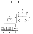
- FIG. 1 is a block diagram of an optical transmitter illustrating an embodiment of the present invention.
- Reference numeral 2 denotes a laser diode
- 4 denotes a bias circuit for supplying a bias current to the laser diode 2
- 6 denotes a modulation circuit for superposing modulation current pulses corresponding to an input signal on the bias current
- 8 denotes a Mach-Zehnder optical interferometer (MZ optical interferometer) for converting phase-modulated light from the laser diode 2 into intensity-modulated light.
- MZ optical interferometer Mach-Zehnder optical interferometer
- the bias current is set to a value higher than the threshold value for oscillation of the laser diode 2.
- the amplitude and pulse width of the modulation current pulses are set so that the integrated value of the oscillation frequency of the laser diode 2 varied by each one of the modulation current pulses becomes a phase amount ⁇ or - ⁇ .
- the MZ optical interferometer 8 splits entering light through an input port 12 into two component light waves to pass through a first and a second optical path.
- the component light waves passing through the first and second optical paths are then allowed to interfere with each other and output from an output port 14.
- the thus output intensity-modulated light is transmitted over an optical transmission line, not shown.
- the first optical path is that through which the light input to the input port 12 is passed, transmitted by a half mirror 16 and a half mirror 18 in order of mention, to reach the output port 14.
- the second optical path is that through which the light input to the input port 12 is passed, reflected by the half mirror 16, a mirror 20, a mirror 22, and the half mirror 18 in order of mention, to reach the output port 14.
- the time difference between the propagation delays in the first and second optical paths is set to the time period corresponding to one time slot of the modulation current pulses (or the input signal).
- Reference numeral 10 denotes a periodic signal superposing circuit for superposing a periodic signal on the bias current.
- the period of the periodic signal corresponds to one time slot of the modulation current pulses (or the input signal).
- the periodic signal is a sine or cosine wave signal.
- the output of the MZ optical interferometer 8 depends on the phase difference between the component light waves which pass through the first optical path and the second optical path and interfere with each other. If the phase difference is fixed at ⁇ (or (2n + 1) ⁇ , where n is an integer), then no power will be output. When the phase of the light wave input to the MZ optical interferometer 8 changes in one time slot, the output intensity will change.
- FIG. 2A is a waveform chart showing the frequency shift, and an RZ type waveform is obtained there.
- RZ type in this case, it is only meant that the signal level returns to zero every modulation time slot, and the duty ratio can be of any value. In an extreme case where the duty ratio is 1, the waveform will become a rectangular waveform of an NRZ type.
- the phase shift for a signal "1" during one time slot can be set to ⁇ as shown in FIG. 2B by setting the amplitude of the modulation current pulses to a suitable value.
- This light wave is allowed to interfere with the light wave delayed by one time slot with equal amplitude in the MZ optical interferometer 8.
- the phase of the light wave delayed by one time slot is indicated by a broken line in FIG. 2B.
- the initial phase of the delayed light wave may be set at zero or ⁇ (the initial phase in FIG. 2B is set at ⁇ ).
- the output intensity of the MZ optical interferometer 8 is determined by the phase difference between the two interfering light waves.
- the phase difference is represented by the difference between the solid line and the broken line in FIG. 2B, which becomes as shown in FIG. 2D and varies between zero and ⁇ .
- the light output reaches a maximum when the phase difference is zero and the light output becomes zero when the phase difference is ⁇ . Accordingly, the intensity waveform of the light output becomes as shown in FIG. 2E.
- the output waveform is corresponding to the input signal, there is a delay in time corresponding to half of one time slot between the output signal and the input signal. Further, the output waveform is of an NRZ type regardless of the duty ratio of the RZ input signal. The duty ratio of the input signal determines the rise time and the fall time in the output waveform.
- FIG. 2C shows the additional phase given by the periodic signal when the periodic signal is a sine wave. Since the period of the periodic signal is concurrent with the period of the modulation current pulses, the value of the additional phase is equal for each time slot. Further, the additional phase is given to both of the light waves propagating through the first and the second paths. Accordingly, even when the periodic signal is superposed on the bias current, the phase difference as shown in FIG. 2D, as in the case where the periodic signal was not superposed, is produced. As a result, intensity-modulated light corresponding to the input signal can be obtained.
- the effect of the wavelength dispersion is understood to cause a phenomenon of the pulse width of a light pulse, which is infinitely close to zero when the light pulse enters an optical fiber, becoming broadened when the light pulse is output from the emission end of the optical fiber. This phenomenon in general leads to an adverse effect but not always does so.
- a sine or cosine wave signal is used so that the effect of the wavelength dispersion contributes to an improvement in the transmission waveform.
- the generation of the periodic signal is easy when a sine or cosine wave signal is used for the periodic signal.
- the degree of improvement in the transmission waveform by the superposition of the periodic signal depends on its amplitude and phase. It is therefore desired that the amplitude and phase of the sine or cosine wave signal are set such that the improvement in the transmission waveform becomes most remarkable.
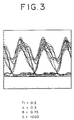
- FIG. 3 is a diagram showing results of a simulation of the eye pattern.
- the duty ratio Tr of the modulation current pulses was 0.5
- the constant A in the above expression was 0.3 (radian)
- the constant B therein was 0.75
- the wavelength dispersion coefficient D of the optical transmission path was 1000 ps/nm. It is apparent from the diagram that the transmission waveform is improved.
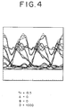
- FIG. 4 shows results of a simulation of the eye pattern when the periodic signal was not superposed.
- the transmission waveform is greatly improved by the present embodiment.
- the present invention has been described above as related to specific embodiments, the present invention is not limited to the details of such embodiments.
- the optical interferometer other types of optical interferometers than the Mach-Zehnder type optical interferometer, such as Michelson type and Fabry-Perot type optical interferometer can be used.
- the periodic signal other signals than sine or cosine wave signal, such as a triangular wave signal and a square wave signal can be used provided that they are capable of making the effect of the wavelength dispersion improve the transmission waveform.
Landscapes
- Physics & Mathematics (AREA)
- Optics & Photonics (AREA)
- Electromagnetism (AREA)
- Engineering & Computer Science (AREA)
- Computer Networks & Wireless Communication (AREA)
- Signal Processing (AREA)
- Optical Communication System (AREA)
- Semiconductor Lasers (AREA)
Applications Claiming Priority (2)
| Application Number | Priority Date | Filing Date | Title |
|---|---|---|---|
| JP411004/90 | 1990-12-17 | ||
| JP2411004A JP2970776B2 (ja) | 1990-12-17 | 1990-12-17 | 光送信装置 |
Publications (3)
| Publication Number | Publication Date |
|---|---|
| EP0491272A2 true EP0491272A2 (fr) | 1992-06-24 |
| EP0491272A3 EP0491272A3 (en) | 1993-11-18 |
| EP0491272B1 EP0491272B1 (fr) | 1998-08-12 |
Family
ID=18520078
Family Applications (1)
| Application Number | Title | Priority Date | Filing Date |
|---|---|---|---|
| EP91121257A Expired - Lifetime EP0491272B1 (fr) | 1990-12-17 | 1991-12-11 | Emetteur optique |
Country Status (5)
| Country | Link |
|---|---|
| US (1) | US5379144A (fr) |
| EP (1) | EP0491272B1 (fr) |
| JP (1) | JP2970776B2 (fr) |
| CA (1) | CA2057572C (fr) |
| DE (1) | DE69129977T2 (fr) |
Cited By (1)
| Publication number | Priority date | Publication date | Assignee | Title |
|---|---|---|---|---|
| USRE36088E (en) * | 1990-03-01 | 1999-02-09 | Fujitsu Limited | Optical transmitter |
Families Citing this family (6)
| Publication number | Priority date | Publication date | Assignee | Title |
|---|---|---|---|---|
| JP2655508B2 (ja) * | 1995-03-07 | 1997-09-24 | 日本電気株式会社 | 光送信回路 |
| US5612973A (en) * | 1995-06-19 | 1997-03-18 | Massachusetts Institute Of Technology | System employing dissipative pseudorandom dynamics for communications and measurement |
| JP3620966B2 (ja) * | 1998-06-30 | 2005-02-16 | 富士写真フイルム株式会社 | 半導体レーザ励起固体レーザ |
| JP4146800B2 (ja) * | 2002-01-09 | 2008-09-10 | 株式会社アドバンテスト | 位相変調回路、試験装置、及び通信システム |
| GB0805786D0 (en) * | 2008-03-31 | 2008-04-30 | Filtronic Plc | Methods of modulating a quantum dot laser and a multisection dot laser |
| US8781336B1 (en) * | 2011-02-10 | 2014-07-15 | Finisar Corporation | Optical filter for use in a laser transmitter |
Family Cites Families (6)
| Publication number | Priority date | Publication date | Assignee | Title |
|---|---|---|---|---|
| JPH0810848B2 (ja) * | 1986-05-02 | 1996-01-31 | 日本電気株式会社 | 光送信器 |
| US4805235A (en) * | 1986-02-17 | 1989-02-14 | Nec Corporation | Optical transmitter comprising an optical frequency discriminator |
| US4754452A (en) * | 1986-09-11 | 1988-06-28 | American Telephone And Telegraph Company, At&T Bell Laboratories | Optical local area network using a common optical carrier with separate user angle modulation |
| US5025487A (en) * | 1987-01-20 | 1991-06-18 | Gte Laboratories Incorporated | System for transmitting information on interferometrically generated optical carriers |
| JPS648356A (en) * | 1987-06-30 | 1989-01-12 | Japan Electronic Control Syst | Ignition timing controller of internal combustion engine |
| WO1989008356A1 (fr) * | 1988-03-04 | 1989-09-08 | Fujitsu Limited | Procede et dispositif de modulation d'un laser a semi-conducteur |
-
1990
- 1990-12-17 JP JP2411004A patent/JP2970776B2/ja not_active Expired - Fee Related
-
1991
- 1991-12-11 DE DE69129977T patent/DE69129977T2/de not_active Expired - Fee Related
- 1991-12-11 EP EP91121257A patent/EP0491272B1/fr not_active Expired - Lifetime
- 1991-12-13 CA CA002057572A patent/CA2057572C/fr not_active Expired - Fee Related
-
1993
- 1993-11-17 US US08/153,494 patent/US5379144A/en not_active Expired - Lifetime
Cited By (1)
| Publication number | Priority date | Publication date | Assignee | Title |
|---|---|---|---|---|
| USRE36088E (en) * | 1990-03-01 | 1999-02-09 | Fujitsu Limited | Optical transmitter |
Also Published As
| Publication number | Publication date |
|---|---|
| CA2057572C (fr) | 1996-03-26 |
| CA2057572A1 (fr) | 1992-06-18 |
| DE69129977T2 (de) | 1999-01-21 |
| EP0491272B1 (fr) | 1998-08-12 |
| DE69129977D1 (de) | 1998-09-17 |
| EP0491272A3 (en) | 1993-11-18 |
| JP2970776B2 (ja) | 1999-11-02 |
| JPH04216686A (ja) | 1992-08-06 |
| US5379144A (en) | 1995-01-03 |
Similar Documents
| Publication | Publication Date | Title |
|---|---|---|
| US5434693A (en) | Optical short pulse generating device | |
| US8078062B2 (en) | Carrier-suppressed optical pulse train generating device and method | |
| US5339183A (en) | Optical signal transmission device | |
| EP0430230B1 (fr) | Appareil de transmission optique | |
| US7564889B2 (en) | Adiabatically frequency modulated source | |
| JP3268994B2 (ja) | デジタルデータの光学的伝送方法 | |
| JP2917333B2 (ja) | 光送信方法及び光送信装置 | |
| US6262834B1 (en) | Wideband single sideband modulation of optical carriers | |
| EP0404054B1 (fr) | Procédé et système de modulation directe à déplacement de phase | |
| US6341031B1 (en) | Optical pulse generation using a high order function waveguide interferometer | |
| US20100021182A1 (en) | Optical transmitter | |
| US7099359B2 (en) | Optical pulse train generator | |
| JP3345214B2 (ja) | 短光パルス変調方法およびその装置 | |
| JP3886147B2 (ja) | 分散の補償 | |
| US5889607A (en) | Optical modulator, optical short pulse generating device, optical waveform shaping device, and optical demultiplexer device | |
| US5621560A (en) | Method and system for reducing chirp in external modulation | |
| US6330098B1 (en) | Apparatus for externally modulating two optical channels at the same time | |
| US6493127B2 (en) | Modulation systems using dual channel optical modulators | |
| EP0491272B1 (fr) | Emetteur optique | |
| US6535316B1 (en) | Generation of high-speed digital optical signals | |
| JPS61502842A (ja) | 高速強度変調光源 | |
| CN115144841A (zh) | 一种大带宽线性调频信号产生装置及方法 | |
| JP2003322830A (ja) | 光変調装置及び光変調方法 | |
| JPH1117257A (ja) | 光パルスの発生方法 | |
| JPH07170232A (ja) | 光フィルタ制御回路 |
Legal Events
| Date | Code | Title | Description |
|---|---|---|---|
| PUAI | Public reference made under article 153(3) epc to a published international application that has entered the european phase |
Free format text: ORIGINAL CODE: 0009012 |
|
| AK | Designated contracting states |
Kind code of ref document: A2 Designated state(s): DE FR GB |
|
| PUAL | Search report despatched |
Free format text: ORIGINAL CODE: 0009013 |
|
| AK | Designated contracting states |
Kind code of ref document: A3 Designated state(s): DE FR GB |
|
| 17P | Request for examination filed |
Effective date: 19931110 |
|
| 17Q | First examination report despatched |
Effective date: 19960830 |
|
| GRAG | Despatch of communication of intention to grant |
Free format text: ORIGINAL CODE: EPIDOS AGRA |
|
| GRAG | Despatch of communication of intention to grant |
Free format text: ORIGINAL CODE: EPIDOS AGRA |
|
| GRAH | Despatch of communication of intention to grant a patent |
Free format text: ORIGINAL CODE: EPIDOS IGRA |
|
| GRAH | Despatch of communication of intention to grant a patent |
Free format text: ORIGINAL CODE: EPIDOS IGRA |
|
| GRAA | (expected) grant |
Free format text: ORIGINAL CODE: 0009210 |
|
| AK | Designated contracting states |
Kind code of ref document: B1 Designated state(s): DE FR GB |
|
| REF | Corresponds to: |
Ref document number: 69129977 Country of ref document: DE Date of ref document: 19980917 |
|
| ET | Fr: translation filed | ||
| PLBE | No opposition filed within time limit |
Free format text: ORIGINAL CODE: 0009261 |
|
| STAA | Information on the status of an ep patent application or granted ep patent |
Free format text: STATUS: NO OPPOSITION FILED WITHIN TIME LIMIT |
|
| 26N | No opposition filed | ||
| REG | Reference to a national code |
Ref country code: GB Ref legal event code: IF02 |
|
| PGFP | Annual fee paid to national office [announced via postgrant information from national office to epo] |
Ref country code: GB Payment date: 20061206 Year of fee payment: 16 |
|
| PGFP | Annual fee paid to national office [announced via postgrant information from national office to epo] |
Ref country code: DE Payment date: 20061207 Year of fee payment: 16 |
|
| PGFP | Annual fee paid to national office [announced via postgrant information from national office to epo] |
Ref country code: FR Payment date: 20061208 Year of fee payment: 16 |
|
| GBPC | Gb: european patent ceased through non-payment of renewal fee |
Effective date: 20071211 |
|
| PG25 | Lapsed in a contracting state [announced via postgrant information from national office to epo] |
Ref country code: DE Free format text: LAPSE BECAUSE OF NON-PAYMENT OF DUE FEES Effective date: 20080701 |
|
| REG | Reference to a national code |
Ref country code: FR Ref legal event code: ST Effective date: 20081020 |
|
| PG25 | Lapsed in a contracting state [announced via postgrant information from national office to epo] |
Ref country code: GB Free format text: LAPSE BECAUSE OF NON-PAYMENT OF DUE FEES Effective date: 20071211 |
|
| PG25 | Lapsed in a contracting state [announced via postgrant information from national office to epo] |
Ref country code: FR Free format text: LAPSE BECAUSE OF NON-PAYMENT OF DUE FEES Effective date: 20071231 |