EP0492095A2 - Méthode et appareillage d'usinage de cartes à circuits imprimés, en particulier de cartes équipées d'éléments de surface - Google Patents
Méthode et appareillage d'usinage de cartes à circuits imprimés, en particulier de cartes équipées d'éléments de surface Download PDFInfo
- Publication number
- EP0492095A2 EP0492095A2 EP91118821A EP91118821A EP0492095A2 EP 0492095 A2 EP0492095 A2 EP 0492095A2 EP 91118821 A EP91118821 A EP 91118821A EP 91118821 A EP91118821 A EP 91118821A EP 0492095 A2 EP0492095 A2 EP 0492095A2
- Authority
- EP
- European Patent Office
- Prior art keywords
- soldering
- chamber
- auxiliary
- printed circuit
- solder
- Prior art date
- Legal status (The legal status is an assumption and is not a legal conclusion. Google has not performed a legal analysis and makes no representation as to the accuracy of the status listed.)
- Granted
Links
Images

Classifications
-
- B—PERFORMING OPERATIONS; TRANSPORTING
- B23—MACHINE TOOLS; METAL-WORKING NOT OTHERWISE PROVIDED FOR
- B23K—SOLDERING OR UNSOLDERING; WELDING; CLADDING OR PLATING BY SOLDERING OR WELDING; CUTTING BY APPLYING HEAT LOCALLY, e.g. FLAME CUTTING; WORKING BY LASER BEAM
- B23K1/00—Soldering, e.g. brazing, or unsoldering
- B23K1/08—Soldering by means of dipping in molten solder
- B23K1/085—Wave soldering
-
- B—PERFORMING OPERATIONS; TRANSPORTING
- B23—MACHINE TOOLS; METAL-WORKING NOT OTHERWISE PROVIDED FOR
- B23K—SOLDERING OR UNSOLDERING; WELDING; CLADDING OR PLATING BY SOLDERING OR WELDING; CUTTING BY APPLYING HEAT LOCALLY, e.g. FLAME CUTTING; WORKING BY LASER BEAM
- B23K1/00—Soldering, e.g. brazing, or unsoldering
- B23K1/20—Preliminary treatment of work or areas to be soldered, e.g. in respect of a galvanic coating
- B23K1/206—Cleaning
-
- C—CHEMISTRY; METALLURGY
- C23—COATING METALLIC MATERIAL; COATING MATERIAL WITH METALLIC MATERIAL; CHEMICAL SURFACE TREATMENT; DIFFUSION TREATMENT OF METALLIC MATERIAL; COATING BY VACUUM EVAPORATION, BY SPUTTERING, BY ION IMPLANTATION OR BY CHEMICAL VAPOUR DEPOSITION, IN GENERAL; INHIBITING CORROSION OF METALLIC MATERIAL OR INCRUSTATION IN GENERAL
- C23G—CLEANING OR DE-GREASING OF METALLIC MATERIAL BY CHEMICAL METHODS OTHER THAN ELECTROLYSIS
- C23G5/00—Cleaning or de-greasing metallic material by other methods; Apparatus for cleaning or de-greasing metallic material with organic solvents
-
- H—ELECTRICITY
- H05—ELECTRIC TECHNIQUES NOT OTHERWISE PROVIDED FOR
- H05K—PRINTED CIRCUITS; CASINGS OR CONSTRUCTIONAL DETAILS OF ELECTRIC APPARATUS; MANUFACTURE OF ASSEMBLAGES OF ELECTRICAL COMPONENTS
- H05K3/00—Apparatus or processes for manufacturing printed circuits
- H05K3/30—Assembling printed circuits with electric components, e.g. with resistors
- H05K3/32—Assembling printed circuits with electric components, e.g. with resistors electrically connecting electric components or wires to printed circuits
- H05K3/34—Assembling printed circuits with electric components, e.g. with resistors electrically connecting electric components or wires to printed circuits by soldering
- H05K3/3489—Composition of fluxes; Application thereof; Other processes of activating the contact surfaces
-
- B—PERFORMING OPERATIONS; TRANSPORTING
- B23—MACHINE TOOLS; METAL-WORKING NOT OTHERWISE PROVIDED FOR
- B23K—SOLDERING OR UNSOLDERING; WELDING; CLADDING OR PLATING BY SOLDERING OR WELDING; CUTTING BY APPLYING HEAT LOCALLY, e.g. FLAME CUTTING; WORKING BY LASER BEAM
- B23K2101/00—Articles made by soldering, welding or cutting
- B23K2101/36—Electric or electronic devices
- B23K2101/40—Semiconductor devices
Definitions
- the invention relates to a method for soldering electronic printed circuit boards, in particular printed circuit boards equipped with components, according to the preamble of patent claim 1, and to an apparatus for carrying out this method according to the preamble of patent claim 20.
- passive layers are located on the solder connection surfaces, which are oxide layers and organic and / or inorganic contamination layers. These passive layers hinder the access of the solder to the solder connection areas and therefore usually have to be removed, ie removed from the metallic base.
- soldering connection surfaces are wetted with liquid solder
- decapitation device by means of which the oxide layers which are at least present on the soldering connection surfaces are largely removed.
- the flux reacts with the Passive layers and solves them, for example, by complex formation. It also has the task of preventing the passive layers from forming again until they are wetted with liquid solder. It can also reduce the surface tension of the solder and prevent bridging between adjacent solder joints, and finally the flux delays the formation of oxide skins on the fresh solder joints so that they can form in the desired configuration.
- Flux residues can, however, impair the electrical function of the printed circuit board and have a corrosive effect on components and printed circuit boards. In order to ensure reliable electrical function of the printed circuit boards, it is therefore necessary to remove the flux residues after the soldering in a downstream cleaning process.
- a cleaning bath made of fluorinated chlorohydrocarbons (CFCs) or chlorinated hydrocarbons (CHCs) was previously common. The efforts to limit the environmental impact of CFC or CFC-containing fluids have led to high investments in exhaust air and wastewater treatment, which make soldering processes using flux more expensive.
- a method for soldering electronic printed circuit boards (DE-GM 85 20 254) is known, in which the pickling is carried out with the aid of a protective gas, which has an oxide layer-reducing effect and which is preferably a nitrogen-hydrogen mixture.
- the flat module is exposed to this protective gas in a fumigation chamber upstream of the soldering device, which is known in this Case forms the pick-up device.
- the protective layer's reducing effect on oxide layers flux-free soldering of the printed circuit boards should be possible.
- difficulties can be caused by the reducing effect, which is not limited to the oxide layers, by the measures that are necessary to prevent the formation of explosive air / protective gas mixtures, and by the high process temperatures required.
- the invention has for its object to provide a method according to the preamble of claim 1 for soldering electronic printed circuit boards, which does away with the need for decapitating agents in the form of flux and makes the post-treatment cleaning of soldered printed circuit boards unnecessary when using flux. Furthermore, the device according to the preamble of claim 20 is to be developed in such a way that it is suitable for carrying out the new method. This task is fiction, regarding the method
- a condensable auxiliary is first brought to adsorption in imperfections in the oxide layers and at least partially condensed in the imperfections and then the oxide layers are subjected to such rapid heating that the condensate condensed in the defects evaporates explosively and thereby the The oxide layer breaks open and blows off the metallic surface.
- Oxide layer structures generally have an accumulation of three-dimensional layer defects, which can increase, among other things, with the layer thickness.
- the total surface of this Three-dimensional layer defects in the form of microscopic profiles, gaps and holes in the otherwise closed surface exceeds the level projection surface of a solder connection surface many times over.
- these imperfections are now used to adsorb on the surfaces of an initially gaseous auxiliary which then condenses at least partially in the imperfections and thereby fills the imperfections with liquid. If heat is then quickly added to the oxide layers later, the liquid in the defects evaporates suddenly. This is inevitably accompanied by a large increase in the volume of the excipient.
- the mechanism of action of the method according to the invention described above is thus the rapid volume expansion of the auxiliary substance absorbed and condensed in the three-dimensional layer defects of the oxide layer.
- the process must therefore be carried out in such a way that it enables the auxiliary to penetrate into the gaps in the gaseous phase and to be adsorbed there, that the auxiliary then condenses in the missing and that finally enough heat reaches the condensed auxiliary so that it Volume explosive increases.
- These conditions for carrying out the process are relatively easy to meet: if the free surface of the oxide layer is sufficiently hydrophilic, it is sufficient to expose the solder connection surfaces to a gas atmosphere containing the auxiliary substance under suitable pressure and at a suitable temperature so that the auxiliary substance penetrates into the defects, there is adsorbed and finally condensed.
- the required rapid heating of the oxide layers is also not a fundamentally difficult problem.
- the oxide layers are seized by physically blasting them off in the micro range. A flux is not required for this.
- the method according to the invention thus enables flux-free soldering. Chemical reaction products do not occur with this type of paper removal, so that they do not have to be removed and cannot lead to soldering errors. Since the mechanism of action takes advantage of the special structural properties of the oxide layers, the base material surfaces underneath the oxide layer are not attacked when the paper is removed. Finally, it should be noted that the older and the thicker an oxide layer, the more imperfections in which the expandable auxiliary substance can be introduced. In other words, this means that an oxide layer, to the extent that it appears thicker and more disruptive, is at the same time more and more vulnerable to attack and removal in the manner provided according to the invention. This is a clear difference to wet chemical pickling using a flux or to pickling using a protective gas that reduces oxide layers.
- the auxiliary used should have a low molecular weight and should be polar so that it is in gaseous form Condition can diffuse into the defects and is adsorbed there.
- the boiling point of the auxiliary is preferably above room temperature.
- auxiliaries are water, methanol, acetone and ethanol, although this list of auxiliaries is not exhaustive.
- the entire assembled printed circuit board is preferably exposed to a gas atmosphere containing the auxiliary in the gaseous phase, which can be air with water as auxiliary.
- the condition pressure, temperature, relative humidity
- the condition must be such that the auxiliary in the gaseous phase can penetrate into the pores formed by the defects and can be adsorbed there.
- An early drop formation on the surface of the oxide layer could result in the pores being closed by the drop formation and the gaseous auxiliary material not being able to diffuse into the defects. Such early drop formation is therefore inappropriate.
- the gas mixture of air and the auxiliary especially when the auxiliary is water, has the great advantage of simply providing this gas atmosphere and the maximum possible environmental compatibility.
- a pure auxiliary atmosphere is also possible, for example an atmosphere made of 100% water vapor.
- the auxiliary substance condensed in the defects should evaporate suddenly or explosively in the process according to the invention. This presupposes that at the point in time at which the rapid heating takes place there is still a sufficient amount of liquid in the auxiliary in the oxide layer. It must therefore be prevented that the condensed Auxiliary gradually evaporates and escapes before rapid heating.
- the gradual evaporation of the auxiliary substance can be prevented in a simple manner by the rapid heating of the adsorption and condensation of the auxiliary substance occurring at a short time interval and / or by the joining partners being exposed to such conditions after the condensation of the auxiliary substance until rapid heating, for example in a climatic chamber are that there is no evaporation of the auxiliary.
- the temperature gradient over time in the oxide layer is preferably above 50 K / s, in particular above 150 K / s. Much higher temperature gradients of up to 500 K / s are also suitable and can be implemented.
- the supply of heat for the purpose of rapid heating can take place by means of any suitable device, for example by means of an IR heating device and by means of a laser heating device. If such a heating device is used, this is preferably done in a protective gas atmosphere so that the virginity of the soldered connection surfaces generated by the blasting off of the oxide layers is retained.
- the heat supply for the purpose of rapid heating of the oxide layer ie its heating, can take place immediately before the soldering process. Alternatively, it can also be carried out at a certain time interval before the soldering process, in which case, however, the virgin surface created must preferably be maintained in a protective gas atmosphere until the soldering process.
- the oxide layer with the adsorbed auxiliary is heated during the soldering process by thermal energy contained in or supplied to the solder.
- the soldering process anyway requires heat to be supplied to the solder so that it is in the liquid phase and can wet the solder connection surfaces. If - as is preferably provided - the amount of heat for the rapid heating of the oxide layer is taken from this heat supply, no process step separated from the soldering process is necessary for rapid heating, but this process step takes place, while the solder connection surfaces anyway immediately before and during the wetting be heated with the liquid solder.
- the above-mentioned manner can be used, for example, for laser soldering or resistance pulse soldering.
- the heat input directly from the solder wave during wave soldering is particularly advantageous. If the method according to the invention is carried out in connection with a wave soldering process, this can be done in such a way that the assembled printed circuit board slides onto the standing solder wave without the oxide layers having been removed from the solder connection surfaces beforehand, but the condensed auxiliary substance already being in the oxide layers has been introduced. If a certain surface element of a solder connection surface is considered when passing through the solder wave, it results for this surface element that it is heated abruptly on first contact with the solder wave, so that the explosive volume expansion of the auxiliary material and explosion of the oxide layers already described takes place.
- the blasted oxide layers are washed away by the solder wave.
- the virgin solder connection surface exposed under the blasted off oxide layer is removed without delay from of the solder wave, so that the solder wave itself fulfills a protective fluid function and, for example, a renewed oxide formation is excluded.
- this protective covering of the virgin solder connection surfaces their wetting by the solder begins.
- the above-described adsorption of the gaseous auxiliary in the defects presupposes that it can get into the defects and that the surfaces on which the auxiliary is to be adsorbed are sufficiently hydrophilic.
- the oxide layers on the solder connection surfaces are frequently contaminated by further passive layers of organic and / or inorganic type, so that the oxide layer surfaces have no free bonds because they are saturated by impurities and are hydrophobic.
- a pretreatment to remove passive layers on the oxide layers is carried out during the decapitation process before the adsorption of the auxiliary. This is intended to expose the pores in the oxide layer, insofar as they are covered by the passive layers, and to make the surface of the oxide layers hydrophilic.
- This hydrophilization can be carried out in a wet chemical manner with the aid of a cleaning agent, it being understood that the aggressiveness of this cleaning agent and the resulting pollution can be lower than in the case of a flux, which, in addition to the organic and inorganic contamination layers, is also intended to remove the oxide layers.
- the pretreatment is carried out with the aid of a plasma to which the soldering connection surfaces are exposed.
- a plasma pretreatment Due to the German patent application P 39 36 955.2, flat assemblies are part of the prior art, in which case the complete removal, including the oxide layers, is sought by means of a plasma pretreatment.
- the plasma pretreatment for the hydrophilization and not for the removal of the oxide layers takes place within the scope of the invention, so that a reducing effect of the plasma is not important.
- the plasma pretreatment potentially and homogeneously supports cavitation, ie the exposure of existing topology disorders.
- Suitable process gases for the plasma are O2, N2, H2, CO2, N2O and H2O and in particular air, preferably a low-pressure plasma.
- the state obtained by the hydrophilization should also be present at the time when the auxiliary is adsorptively incorporated. It can therefore be provided in an advantageous embodiment of the invention that between the plasma pretreatment and the adsorptive storage of the auxiliary substance, the printed circuit board is ventilated in hydrocarbon-free air. Freedom from oxygen is not required at this point in time, since the oxide layers are still present on the solder connection areas anyway. However, it has been shown that even storing the plasma-pretreated joining partners for several hours under ambient conditions does not yet make the solder connection surfaces unsuitable for the subsequent treatment.
- the device for soldering electronic printed circuit boards has a humidification chamber in which a gas atmosphere is present which contains the gaseous, condensable auxiliary.
- the printed circuit board remains in this humidification chamber during a controllable treatment period.
- the state conditions of the gas atmosphere can be set such that the auxiliary substance is absorbed in the oxide layers on the solder connection surfaces of the parts to be joined and at least partially condensed.
- the device according to the invention is characterized by a heating device, by means of which the oxide layers are quickly heated following the moistening by adsorption and condensation of the auxiliary.
- the humidification chamber has the advantage that the condition conditions during the humidification can be controlled with sufficient accuracy so that interference can be suppressed and the humidification leads to reproducible results.
- humidification i.e. storage of the condensed auxiliary in the imperfections of the oxide layers, preferably and advantageously preceded by a plasma pretreatment.
- This plasma pretreatment can take place in the humidification chamber, which is then operated in such a way that the gas atmosphere or a process gas atmosphere for the plasma pretreatment is optionally produced in it.
- This design of the device makes it possible, in particular, to use the method according to the invention even with a small number of printed circuit boards to be soldered with little expenditure on the device.
- the pickling device in addition to the humidification chamber has a process chamber for plasma pretreatment of the solder pads.
- this comprises, in series, an evacuation chamber, the process chamber for plasma pretreatment, an aeration chamber in which the plasma-pretreated printed circuit boards are aerated with hydrocarbon-free air, the humidification chamber and, as a soldering device, a wave soldering device which generates at least one standing solder wave , wherein all the above-mentioned chambers are designed as flow-through chambers and can be separated from one another by locks.
- the humidification chamber also serves as a preheating device for the soldering process and the wave soldering device simultaneously forms the heating device for the oxide layers with the incorporated auxiliary.
- the soldering device is not necessarily a wave soldering device; rather, it can also be a soldering device with a static solder bath or a reflow soldering device, for example.
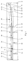
- each flat assembly 4 comprises a printed circuit board 6 which is equipped with components, not shown, which may be pluggable and / or attachable components, for example.
- Each circuit board 6 can be held by a solder frame, not shown.
- the circuit boards 6 are transported through the device with the aid of successively arranged transport devices 8, 10, 12, 14 and 16, which are, for example, belt or chain conveyor devices which engage on the lateral edges of the printed circuit boards. Details of these transport devices are not explained in detail here, since their training is not important for the invention.
- the transport device 8 transfers the transported flat assemblies 6 to the transport device 10, this transfers them to the transport device 12, the latter transfers to the transport device 14 and this transfers to the transport device 16.
- the transport devices 8, 10 and 12 transport the flat assemblies 4 on an essentially horizontal path.
- the transport path defined by the transport device 14 rises slightly at its rear end.
- the transport device 16 also defines a slightly rising transport path.
- the printed circuit boards 6 which have been conventionally equipped and have not yet been removed are first introduced into an evacuation chamber 18 which is located at the left end of the device in FIG. 1, at which the device is loaded with the printed circuit boards 4 in any suitable manner Way is done.
- the evacuation chamber 18 is designed as a tunnel-shaped flow chamber and accordingly has an inlet at its left end and an outlet at its right end.
- the inlet can be closed by means of a first lock 20, which is designed, for example, as a vertically displaceable plate.
- the outlet of the evacuation chamber 18 can be closed by means of a second lock 22 which, like the other locks of the device, can also be designed as a vertically displaceable plate.
- the first transport device 8 is arranged within the evacuation chamber 18 such that it can transport the printed circuit boards 4 in a predetermined manner from the inlet to the outlet through the evacuation chamber 8.
- the interior of the evacuation chamber 18 is connected to a vacuum pump 24, by means of which the evacuation chamber 18 can be evacuated to a desired negative pressure when the locks 20 and 22 are closed.
- This negative pressure is, for example, the process pressure of 30 to 40 Pa within a process chamber 26 to be explained for a plasma pretreatment.
- the evacuation chamber 18 is also provided with a ventilation system which makes it possible to increase the pressure inside the evacuation chamber 18 to the ambient pressure or to a pressure in the region of the ambient pressure.
- the process chamber 26 for a plasma pretreatment is connected to the evacuation chamber 18.
- the process chamber 26 is also provided with an inlet and an outlet as a continuous chamber, its inlet being second by means of the same Lock 22 is closable, which serves as a closure of the outlet of the evacuation chamber 18.
- the outlet of the process chamber 26 can be closed by means of a third lock 28.
- Arranged within the process chamber 26 is the second transport device 10, to which the printed circuit boards 4 are transferred by the first transport device 24 when the first and third locks 20 and 28 and the second lock 22 are open.
- the process chamber 26 is connected to a vacuum pump 30, with the aid of which the inside of the process chamber 26 can be evacuated to the process pressure of, for example, 30 to 40 Pa.
- the process chamber 26 can be ventilated.
- the aeration of the process chamber 26 is, however, only carried out when the entire device is switched off.
- the process chamber 26 is always under process pressure and is always filled with process gas, since the supply of printed circuit boards 4 to the process chamber 26 and the removal of the printed circuit boards from this always takes place in or in chambers which are also evacuated to the process pressure.
- the process chamber 26 is provided with devices, not shown, which make it possible to generate and maintain a low-pressure plasma within the process chamber 26.
- These devices include the gas connections with which the process gas is introduced into and discharged from the process chamber 26, heating devices with which the process chamber 26 is brought to the process temperature, and circulation devices for the process gas which circulate it through the process chamber 26 lead and possibly have a gas cleaning system with, for example, an adsorber.
- a low-pressure plasma is generated and maintained in operation, the process gas of O2, N2, H2, CO2, N2O, H2O or a combination of these Gases.
- the process gas can also be air.
- the devices for excitation of the plasma can be, for example, magnetrons, via which the radio-frequency energy for generating the gas plasma is introduced and which are arranged above the transport device 10 in the region of the upper wall of the process chamber 26.
- the process chamber 26 is followed by an aeration chamber 32, which in turn is designed as a continuous chamber with an inlet and an outlet.
- the inlet of the ventilation chamber 32 can be closed by means of the third lock 23, which also serves to close the outlet of the process chamber 26.
- the outlet of the ventilation chamber 32 can be closed by means of a fourth lock 34.
- the third transport device 12 is arranged within the ventilation chamber 32, which takes over the printed circuit boards from the second transport device 10 and passes them on to the fourth transport device 14.
- the ventilation chamber 32 is connected to a further vacuum pump 36, by means of which the interior of the ventilation chamber can be evacuated to the process pressure of the process chamber 26.
- the ventilation chamber 30 is ventilated with the aid of hydrocarbon-free air of defined humidity under ambient pressure.
- the ventilation chamber 32 is evacuated when the third lock 28 is opened so that the printed circuit boards 4 can be transferred from the process chamber 26 into the ventilation chamber 32. At this point, the two locks 22 and 34 are closed.
- the ventilation chamber 32 is under ambient pressure if the fourth lock 34 is open so that the printed circuit boards 4 can be transferred from the ventilation chamber 32 into a humidification chamber 38, which will be explained later.
- the lock 28 is closed so that the process pressure can always be maintained in the process chamber 26.
- the humidification chamber 38 directly adjoins the ventilation chamber 32. This in turn is designed as a flow chamber and has an inlet 40 and an outlet 42. Since the interior of the humidification chamber 38 is always under ambient pressure during operation, the inlet 40 and the outlet 42 cannot be closed and are always open.
- the fourth transport device 14 is arranged within the humidification chamber 38, to which the printed circuit boards 4 are transferred by the third transport device 12 when the fourth lock 34 is open. The fourth transport device 14 transfers the flat modules 4 at the outlet 42 to the fifth transport device 16.
- a gas atmosphere which, in the exemplary embodiment shown, consists of air with a water content in the gaseous phase.
- Associated with the humidification chamber 38 are devices (not shown) for air conditioning the air atmosphere within the humidification chamber 38, which ensure the desired conditions, in particular the desired temperature and the desired relative humidity.
- the temperature is above the ambient temperature in a range of, for example, 40 to 50 ° C.
- a heating device (not shown) is preferably arranged in the humidification chamber, which is also used for preheating the printed circuit boards in preparation for the subsequent actual ones Soldering process is used.
- a first nozzle device 44 is arranged in the region of the inlet 40 of the humidification chamber 38.
- a second nozzle device 46 is arranged in the region of the outlet 42. Cleaned air is blown out through these two nozzle devices, so that an air curtain is generated at the inlet and at the outlet. In this way, on the one hand, the gas atmosphere within the humidification chamber 38 is separated from the environment.
- suitable temperature control of the air curtain generated by the nozzle device 46 it can be ensured that the temperature of the oxide layers on the solder connection surfaces of the printed circuit boards 4 drops below the dew point, so that the condensation of the water adsorbed in the defects in the oxide layers is thereby supported.
- the humidification chamber 38 can be divided into two successive chamber sections, in which case the chamber section closer to the outlet 42 is then kept at a lower temperature than the first chamber section in order to support the aforementioned condensation.
- soldering device 48 Immediately behind the humidification chamber 38 in the direction in which the printed circuit boards 4 pass through is a soldering device 48, which in the exemplary embodiment shown is designed as a wave soldering device. It comprises a crucible 50, in which molten solder is located during operation. Furthermore, it comprises two shafts 52 and 54, each of which has at its upper end a slit-shaped outlet opening running transversely to the transport direction Y of the flat modules 4. Liquid solder is conveyed upwards through these shafts by means of a pump device, not shown, so that the solder emerging through the outlet openings forms a standing solder wave (not shown) there.
- the underside of the respective printed circuit board 6 touches the crests of the solder waves, so that the underside of the printed circuit board is wetted with solder and the SMD components projecting from the underside and connections of THM components into it Immerse plumb.
- the solder wets the surfaces of the parts to be joined or the solder connection surfaces and forms the cohesive bonding characteristic.
- a protective gas inflator which is not provided in this exemplary embodiment and which can follow the soldering device 48 and by means of which a protective gas, in particular nitrogen, is applied to the soldering points immediately after the soldering process.
- the evacuation chamber 18, the process chamber 26, the ventilation chamber 32 and the humidification chamber 38 all belong to the decapitation device in which a two-stage decapitation process is carried out.
- One stage of this pickling process is formed by the plasma pretreatment in the process chamber 26. This removes inorganic and organic passive layers from the oxide layers on the solder pads.
- the other stage of this pickling process is initiated in the humidification chamber 38, in which the gaseous auxiliary substance in the form of water is first introduced into the defects in the oxide layers for adsorption and is then condensed.
- the pickling is only completed in the soldering device 48 at the point in time at which the circuit board under consideration runs onto the first solder wave in the direction of passage. Only at this point does the sudden Heating of the oxide layer with the embedded auxiliary, whereby the oxide layer is blasted off the metallic base of the solder connection surface.
- the soldering device thus simultaneously forms the heating device of the pickling device.
- soldering device also forms the heating device of the decapitation device. Rather, an additional, separate heating device could be arranged between the humidification chamber 38 and the soldering device 48.
- the pluggable components are positively fixed on a wave-solderable layout.
- the flat assemblies 6 prepared in this way are subjected to a dry chemical pretreatment during a first stage of the combined pickling process.
- process gases such as O2, N2, H2, CO2 or N2O and suitable combinations of these gases and air can be used.
- Determined the type of process gas the choice of plasma parameters.
- the selection of the plasma atmosphere and parameters depends on the type and expected thickness of the mainly organic contamination layers on the solder connection surfaces and on the activation of the surfaces of the parts to be joined, which is required by joining technology.
- the plasma pretreatment ensures the homogeneous removal of the organic passive or contamination layers on the solder connection surfaces and the activation of the surfaces of the oxide layers on the solder connection surfaces necessary to ensure a high solder spread and wetting.
- Fig. 2 shows schematically in section a section of a solder pad.
- This has a layer structure, the metallic base material 56 of which consists for example of Sn, SnPb, AgPd or AgPdBi.
- An oxide layer 58 which consists of oxides of the metals of the substrate 56, adheres to the metallic base material 56 before it is removed.
- a predominantly organic contamination layer 60 adheres to the oxide layer 58.
- the oxide layer 58 and the contamination layer 60 together form the passive layers 62, which are removed by the decapitation.
- the solder connection surfaces freed from the organic contamination layers 60 in the process chamber 26 by the plasma pretreatment and thus the entire printed circuit board assembly 4 is subsequently forced-ventilated in the ventilation chamber 32 with a hydrocarbon-free gas atmosphere.
- This hydrocarbon-free gas atmosphere can be hydrocarbon-free air.
- Aeration with nitrogen (N2) has also proven to be suitable.
- the ventilation in the ventilation chamber 32 is intended to prevent organic contamination from occurring again. Under suitable circumstances, this goal can also be achieved if the ventilation takes place with ambient air, although the printed circuit boards should be exposed to the ambient air for only a relatively short time, for example 30 to 600 s.
- the oxide layer 58 exposed and activated by the plasma pretreatment, which consists, for example, of SnPb mixed oxide, on the solder connection surfaces is subsequently fed to the second stage of the combined pickling process.
- the natural topology of the oxide layer 58 has been exposed by the plasma pretreatment.
- This oxide layer 58 has an accumulation of defects 64, the frequency of which increases, among other things, with the layer thickness.
- the total surface of these three-dimensional layer defects or defects is often larger than the area of the projection of the solder connection area under consideration.
- the plasma pretreatment breaks valence bonds that were saturated by the removed organic contamination layer 60. These broken valence bonds characterize the reactivity of the exposed oxide layer. If the pretreated solder pads, which have a thermodynamically unstable oxide layer topology, an atmosphere are exposed, which contains a gaseous, condensable auxiliary, then condensation processes homogeneously distributed will take place according to the frequency of the three-dimensional layer defects.
- the plasma pretreatment has provoked a hydrophilic character of the metal oxides. The hydrophilic metal oxides are therefore surface-saturated in a suitable atmosphere of the type mentioned above by condensation of the auxiliary.
- the process described above, in which the gaseous auxiliary is first adsorbed in the defects and then condensed, can be referred to as humidification and takes place in the humidification chamber 38, in which a gas atmosphere consisting of air with water as auxiliary is present, the relative humidity is at least 30%. Adsorption of air humidity would also occur spontaneously.
- the humidification is preferably carried out in the described humidification chamber 38, which represents a condensation path in terms of process technology.
- the temperature of the water vapor in the humidification chamber 38 is 40 to 85 ° C., preferably 75 to 85 ° C. at normal pressure.
- the residence time in the humidification chamber is, for example, 1 to 30 s and is preferably closer to the upper end of the range mentioned.
- the condensation section also serves as a preheating zone for the printed circuit boards 6, so that the printed circuit boards are also made available for the subsequent soldering process in a temperature-appropriate manner.
- the condensation temperature of the auxiliary used is above the preheating temperature.
- the condensation of the auxiliary in the defects 64 is supported by the air curtain generated at the outlet of the humidification chamber 38 by means of the nozzle device 46.
- the humidification chamber 38 is immediately followed by the soldering device 48 designed as a wave soldering device, to which the printed circuit boards 4 pretreated in the manner described are fed.
- the shortest distances between the humidification chamber 48 and the solder wave generated by means of the first shaft 52 are expedient in order to prevent losses due to adsorption and thus pickling.
- the printed circuit boards 4 treated in the manner described above are thus fed to the (not shown) first solder wave immediately after the condensation path.
- the soldering temperature is, for example, 245 ° C. and the average soldering time is 5 s, for example.
- Fig. 3 the state is shown schematically and enlarged, which results when the assembled and pretreated printed circuit board 6 runs onto the solder wave 66, which is generated in the soldering device 48 by means of the shaft 52.
- the solder wave flows to the left in FIG. 1, ie in the direction of the arrow drawn in the solder wave 66 in FIG. 3.
- the circuit board 6 runs from left to right in FIGS. 1 and 3 onto the solder wave 66, ie in the direction of the arrow drawn in the circuit board 6 in FIG. 3.
- the metallic base 56 of the solder connection surface adheres to the underside of the printed circuit board.
- the oxide layer 58 adheres to this background 56 with a finite number of defined, defined oxides, which are, for example, Sn, Pb and / or SnPb mixed oxides.
- defined oxides which are, for example, Sn, Pb and / or SnPb mixed oxides.
- T / t time of the first contact between them, which is at least a value of 50 K / s, should preferably have more than 150 K / s and in the micro range presumably reaches much higher values.
- the rapid heating of the oxide layer 58 in accordance with the temperature gradient leads to spontaneous evaporation, ie volume expansion of the condensed auxiliary substance stored in the defects 64 in the orthogonal and horizontal oxide layer defect region.
- the auxiliary volume increases, for example, in the case of water (H2O) by a factor of 1000.
- the temperature gradient over time determines the rate of expansion of the adsorbed and condensed auxiliary.
- This spontaneous volume expansion causes a micro-explosion-like detachment of the oxide layer 58 from the metallic base material 56, that is to say, for example, the SnPb layer forming the solder connection surface.
- This second and final stage of the pickling process takes place immediately at the linear entry of the underside of the printed circuit board 6 into the solder wave 66, so that the production of virgin solder connection surfaces takes place approximately at the same time as the wetting of these solder connection surfaces by the liquid solder and thus no wetting-inhibiting passive layers are reproducible Formation of the solder joints between the (not shown in FIG. 3) SMD components and / or THM components on the one hand and the pad or the plated-through hole on the circuit board 6 on the other hand. This process is shown schematically in FIG. 3. The micro-explosions break down the oxide layer 58 into oxide fragments 68, which at the same time are sheared off or lifted off from the metallic substrate 56 by the micro-explosions.
- the blasted off oxide fragments 68 leave the solder connection plane with the solder wave 66 running off, as is explained by the floating oxide fragments 68 shown on the left flank of the solder wave 66 in FIG. 3.
- the oxide layers are blasted off from the solder connection areas of the components.
- the fresh solder joints leaving the second solder wave generated by the shaft 54 are preferably exposed to a protective gas atmosphere, with the aid of which the solder joint topology can be modified in a favorable manner.
- This protective gas is, for example, nitrogen (N2).
- the effect of the above-described pickling process can be influenced in its quantity via the volume of the adsorbed auxiliary and the temperature profile of the soldering device 48, in particular the temperature gradient T / t.
- a condensable auxiliary for example water
- the oxide layers are then subjected to such rapid heating that the auxiliary substance condensed in the flaws evaporates explosively and thereby breaks up the oxide layer and blows off the metallic base material, so that the soldering connection surfaces are brought into a virgin state for the subsequent actual soldering process.
- the rapid heating is preferably carried out by the solder wave itself.
- the device according to the invention has a humidification chamber in which the condensable auxiliary is offered to the hydrophilic oxide layers and is adsorbed by them.
Landscapes
- Engineering & Computer Science (AREA)
- Chemical & Material Sciences (AREA)
- Mechanical Engineering (AREA)
- General Chemical & Material Sciences (AREA)
- Microelectronics & Electronic Packaging (AREA)
- Chemical Kinetics & Catalysis (AREA)
- Manufacturing & Machinery (AREA)
- Materials Engineering (AREA)
- Metallurgy (AREA)
- Organic Chemistry (AREA)
- Electric Connection Of Electric Components To Printed Circuits (AREA)
- Manufacturing Of Printed Wiring (AREA)
- Pressure Welding/Diffusion-Bonding (AREA)
- Finish Polishing, Edge Sharpening, And Grinding By Specific Grinding Devices (AREA)
- Paper (AREA)
Applications Claiming Priority (2)
| Application Number | Priority Date | Filing Date | Title |
|---|---|---|---|
| DE4041270A DE4041270A1 (de) | 1990-12-21 | 1990-12-21 | Verfahren und vorrichtung zur verarbeitung von elektronischen flachbaugruppen, insbesondere mit bauelementen bestueckten leiterplatten |
| DE4041270 | 1990-12-21 |
Publications (3)
| Publication Number | Publication Date |
|---|---|
| EP0492095A2 true EP0492095A2 (fr) | 1992-07-01 |
| EP0492095A3 EP0492095A3 (en) | 1992-08-26 |
| EP0492095B1 EP0492095B1 (fr) | 1993-12-15 |
Family
ID=6421086
Family Applications (1)
| Application Number | Title | Priority Date | Filing Date |
|---|---|---|---|
| EP91118821A Expired - Lifetime EP0492095B1 (fr) | 1990-12-21 | 1991-11-04 | Méthode et appareillage d'usinage de cartes à circuits imprimés, en particulier de cartes équipées d'éléments de surface |
Country Status (7)
| Country | Link |
|---|---|
| US (1) | US5193739A (fr) |
| EP (1) | EP0492095B1 (fr) |
| JP (1) | JPH0851273A (fr) |
| AT (1) | ATE98542T1 (fr) |
| DE (2) | DE4041270A1 (fr) |
| DK (1) | DK0492095T3 (fr) |
| ES (1) | ES2049074T3 (fr) |
Cited By (1)
| Publication number | Priority date | Publication date | Assignee | Title |
|---|---|---|---|---|
| EP0740975A1 (fr) * | 1993-11-09 | 1996-11-06 | Linde Aktiengesellschaft | Soudage à la vaque sans plomb |
Families Citing this family (8)
| Publication number | Priority date | Publication date | Assignee | Title |
|---|---|---|---|---|
| DE4225378A1 (de) * | 1992-03-20 | 1993-09-23 | Linde Ag | Verfahren zum verloeten von leiterplatten unter niederdruck |
| FR2697456B1 (fr) * | 1992-10-30 | 1994-12-23 | Air Liquide | Procédé et dispositif de fluxage par voie sèche. |
| US5499754A (en) * | 1993-11-19 | 1996-03-19 | Mcnc | Fluxless soldering sample pretreating system |
| DE69939072D1 (de) * | 1998-02-27 | 2008-08-21 | Matsushita Electric Industrial Co Ltd | Verfahren zum Trennen des Lötmaterials von der Oxidlötung |
| DE10210217A1 (de) * | 2002-03-08 | 2003-10-16 | Behr Gmbh & Co | Verfahren zum Löten von Aluminium |
| DE10342242A1 (de) * | 2003-09-11 | 2005-04-07 | Behr Gmbh & Co. Kg | Lötwerkstück, Lötverfahren und Wärmetauscher |
| US8844793B2 (en) * | 2010-11-05 | 2014-09-30 | Raytheon Company | Reducing formation of oxide on solder |
| CN117276086A (zh) * | 2023-09-20 | 2023-12-22 | 液化空气(中国)投资有限公司 | 一种表面处理方法 |
Family Cites Families (8)
| Publication number | Priority date | Publication date | Assignee | Title |
|---|---|---|---|---|
| US2136392A (en) * | 1936-06-08 | 1938-11-15 | Murphy Daniel Francis | Method for removing scale from boilers |
| DE1546174A1 (de) * | 1965-03-19 | 1970-02-26 | Otto & Co Gmbh Dr C | Verfahren zum kontinuierlichen Beizen von strangfoermigem Material |
| JPS5315010A (en) * | 1976-07-27 | 1978-02-10 | Nec Corp | Bipolar pulse polarity error detection circuit |
| DE8520254U1 (de) * | 1985-07-11 | 1985-10-31 | Siemens AG, 1000 Berlin und 8000 München | Lötvorrichtung zum Löten elektronischer Flachbaugruppen in einer schutzgasgefüllten Lötkammer |
| DE3824861A1 (de) * | 1988-07-21 | 1990-01-25 | Productech Gmbh | Verfahren zur herstellung von loetverbindungen |
| GB8827933D0 (en) * | 1988-11-30 | 1989-01-05 | Plessey Co Plc | Improvements relating to soldering processes |
| JPH02174190A (ja) * | 1988-12-26 | 1990-07-05 | Hitachi Chem Co Ltd | 電子部品の実装方法 |
| DE4032328A1 (de) * | 1989-11-06 | 1991-09-19 | Wls Karl Heinz Grasmann Weichl | Verfahren und vorrichtung zur verarbeitung von zu verloetenden fuegepartnern |
-
1990
- 1990-12-21 DE DE4041270A patent/DE4041270A1/de not_active Withdrawn
-
1991
- 1991-11-04 ES ES91118821T patent/ES2049074T3/es not_active Expired - Lifetime
- 1991-11-04 AT AT91118821T patent/ATE98542T1/de not_active IP Right Cessation
- 1991-11-04 DE DE91118821T patent/DE59100736D1/de not_active Expired - Fee Related
- 1991-11-04 EP EP91118821A patent/EP0492095B1/fr not_active Expired - Lifetime
- 1991-11-04 DK DK91118821.7T patent/DK0492095T3/da active
- 1991-12-18 US US07/810,708 patent/US5193739A/en not_active Expired - Fee Related
- 1991-12-20 JP JP3338775A patent/JPH0851273A/ja active Pending
Cited By (1)
| Publication number | Priority date | Publication date | Assignee | Title |
|---|---|---|---|---|
| EP0740975A1 (fr) * | 1993-11-09 | 1996-11-06 | Linde Aktiengesellschaft | Soudage à la vaque sans plomb |
Also Published As
| Publication number | Publication date |
|---|---|
| DE59100736D1 (de) | 1994-01-27 |
| JPH0851273A (ja) | 1996-02-20 |
| EP0492095B1 (fr) | 1993-12-15 |
| ATE98542T1 (de) | 1994-01-15 |
| DK0492095T3 (da) | 1994-01-24 |
| EP0492095A3 (en) | 1992-08-26 |
| US5193739A (en) | 1993-03-16 |
| DE4041270A1 (de) | 1992-06-25 |
| ES2049074T3 (es) | 1994-04-01 |
Similar Documents
| Publication | Publication Date | Title |
|---|---|---|
| EP0427020B1 (fr) | Méthode et procédé de traitement de partenaires de joints de brasage | |
| DE69209693T2 (de) | Schwall-Löten in einer Hülle mit schützender Atmosphäre über einem Lötbehälter | |
| DE69917770T2 (de) | Verfahren zum trocknen eines beschichteten substrats | |
| DE102010015841B4 (de) | Reflow-Lötverfahren | |
| DE2411854B2 (de) | Vorrichtung zum Aufbringen von geschmolzenem Lötmittel auf gedruckte Schaltungsplatten | |
| EP0492095B1 (fr) | Méthode et appareillage d'usinage de cartes à circuits imprimés, en particulier de cartes équipées d'éléments de surface | |
| EP1169145B1 (fr) | Procede et dispositif de nettoyage de substrats | |
| DE102007005345B4 (de) | Verfahren zum Reflow-Löten sowie Vorrichtung zur Durchführung des Verfahrens | |
| DE69904787T2 (de) | Verfahren zur Entfernung von Verschmierungen | |
| DE69227277T2 (de) | Verfahren zur Benützung von Lötflussmittel, gedruckte Schaltungsplatte und Verfahren zu seiner Herstellung | |
| DE2003473A1 (de) | Verfahren zur Herstellung gedruckter Schaltungsplatten | |
| DE2908829A1 (de) | Verfahren und vorrichtung zum hartloeten von aluminium unter unterdruck | |
| DE3936955C1 (en) | Plasma treating conductor plates for electronic elements - with process gas e.g. oxygen, hydrogen, fluoro-(chloro)-hydrocarbon, etc. before soldering | |
| EP0445174A1 (fr) | Procede et dispositif de nettoyage d'objets. | |
| DE112017005999B4 (de) | Lötofen und aluminiummaterial-lötverfahren | |
| DE19503186C2 (de) | Chemische Reduzierungslösung für Kupferoxid | |
| DE69703426T2 (de) | Verfahren und Vorrichtung zum Siebdrucken und Löten von elektronischen Bauelementen auf eine gedruckte Leiterplatte | |
| WO1995009255A1 (fr) | Procede de protection contre la corrosion de surfaces brasables en cuivre ou en alliage cuivreux | |
| DE3400879A1 (de) | Verfahren zum verbinden aneinander grenzender metallschichten | |
| DE3328091C1 (de) | Verfahren und Vorrichtung zum kontinuierlichen Reinigen von bestückten, gedruckten Schaltungen und dergleichen | |
| EP0276386B1 (fr) | Procédé pour déposer une couche de soudure sur des surfaces métalliques ou métallisées de composants | |
| EP1412307A2 (fr) | Procede de production de materiaux composites metal-ceramique, notamment de substrats metal-ceramique, et materiau composite metal-ceramique, notamment substrat metal-ceramique produit grace a ce procede | |
| DE60031424T2 (de) | Apparat und methode zur herstellung von mehrschichtigen leiterplatten | |
| DE69603666T2 (de) | Verfahren zum Trockenfluxen von metallischen Fläschen vor dem Löten mit einer Atmosphäre die Wasserdampf enthält | |
| DE2027158A1 (de) | Vorrichtung für die Herstellung gedruckter Schaltungen |
Legal Events
| Date | Code | Title | Description |
|---|---|---|---|
| PUAI | Public reference made under article 153(3) epc to a published international application that has entered the european phase |
Free format text: ORIGINAL CODE: 0009012 |
|
| AK | Designated contracting states |
Kind code of ref document: A2 Designated state(s): AT BE CH DE DK ES FR GB GR IT LI LU NL SE |
|
| PUAL | Search report despatched |
Free format text: ORIGINAL CODE: 0009013 |
|
| AK | Designated contracting states |
Kind code of ref document: A3 Designated state(s): AT BE CH DE DK ES FR GB GR IT LI LU NL SE |
|
| 17P | Request for examination filed |
Effective date: 19920918 |
|
| 17Q | First examination report despatched |
Effective date: 19930309 |
|
| GRAA | (expected) grant |
Free format text: ORIGINAL CODE: 0009210 |
|
| AK | Designated contracting states |
Kind code of ref document: B1 Designated state(s): AT BE CH DE DK ES FR GB GR IT LI LU NL SE |
|
| PG25 | Lapsed in a contracting state [announced via postgrant information from national office to epo] |
Ref country code: GR Free format text: LAPSE BECAUSE OF FAILURE TO SUBMIT A TRANSLATION OF THE DESCRIPTION OR TO PAY THE FEE WITHIN THE PRESCRIBED TIME-LIMIT Effective date: 19931215 |
|
| REF | Corresponds to: |
Ref document number: 98542 Country of ref document: AT Date of ref document: 19940115 Kind code of ref document: T |
|
| REG | Reference to a national code |
Ref country code: DK Ref legal event code: T3 |
|
| REF | Corresponds to: |
Ref document number: 59100736 Country of ref document: DE Date of ref document: 19940127 |
|
| ET | Fr: translation filed | ||
| ITF | It: translation for a ep patent filed | ||
| REG | Reference to a national code |
Ref country code: ES Ref legal event code: FG2A Ref document number: 2049074 Country of ref document: ES Kind code of ref document: T3 |
|
| GBT | Gb: translation of ep patent filed (gb section 77(6)(a)/1977) |
Effective date: 19940412 |
|
| REG | Reference to a national code |
Ref country code: GR Ref legal event code: FG4A Free format text: 3011082 |
|
| PLBE | No opposition filed within time limit |
Free format text: ORIGINAL CODE: 0009261 |
|
| STAA | Information on the status of an ep patent application or granted ep patent |
Free format text: STATUS: NO OPPOSITION FILED WITHIN TIME LIMIT |
|
| PG25 | Lapsed in a contracting state [announced via postgrant information from national office to epo] |
Ref country code: DK Effective date: 19941104 Ref country code: AT Effective date: 19941104 |
|
| REG | Reference to a national code |
Ref country code: DK Ref legal event code: EBP |
|
| PG25 | Lapsed in a contracting state [announced via postgrant information from national office to epo] |
Ref country code: SE Effective date: 19941105 Ref country code: ES Free format text: LAPSE BECAUSE OF EXPIRATION OF PROTECTION Effective date: 19941105 |
|
| PG25 | Lapsed in a contracting state [announced via postgrant information from national office to epo] |
Ref country code: LU Free format text: LAPSE BECAUSE OF NON-PAYMENT OF DUE FEES Effective date: 19941130 Ref country code: BE Effective date: 19941130 |
|
| PGFP | Annual fee paid to national office [announced via postgrant information from national office to epo] |
Ref country code: NL Payment date: 19941130 Year of fee payment: 4 |
|
| 26N | No opposition filed | ||
| EAL | Se: european patent in force in sweden |
Ref document number: 91118821.7 |
|
| PGFP | Annual fee paid to national office [announced via postgrant information from national office to epo] |
Ref country code: DE Payment date: 19950427 Year of fee payment: 4 |
|
| PGFP | Annual fee paid to national office [announced via postgrant information from national office to epo] |
Ref country code: CH Payment date: 19950428 Year of fee payment: 4 |
|
| PGFP | Annual fee paid to national office [announced via postgrant information from national office to epo] |
Ref country code: FR Payment date: 19950509 Year of fee payment: 4 |
|
| BERE | Be: lapsed |
Owner name: WLS KARL-HEINZ GRASMANN Effective date: 19941130 |
|
| REG | Reference to a national code |
Ref country code: GR Ref legal event code: MM2A Free format text: 3011082 |
|
| EUG | Se: european patent has lapsed |
Ref document number: 91118821.7 |
|
| PGFP | Annual fee paid to national office [announced via postgrant information from national office to epo] |
Ref country code: GB Payment date: 19951027 Year of fee payment: 5 |
|
| PG25 | Lapsed in a contracting state [announced via postgrant information from national office to epo] |
Ref country code: LI Effective date: 19951130 Ref country code: CH Effective date: 19951130 |
|
| PG25 | Lapsed in a contracting state [announced via postgrant information from national office to epo] |
Ref country code: NL Effective date: 19960601 |
|
| REG | Reference to a national code |
Ref country code: CH Ref legal event code: PL |
|
| PG25 | Lapsed in a contracting state [announced via postgrant information from national office to epo] |
Ref country code: FR Effective date: 19960731 |
|
| NLV4 | Nl: lapsed or anulled due to non-payment of the annual fee |
Effective date: 19960601 |
|
| PG25 | Lapsed in a contracting state [announced via postgrant information from national office to epo] |
Ref country code: DE Effective date: 19960801 |
|
| REG | Reference to a national code |
Ref country code: FR Ref legal event code: ST |
|
| PG25 | Lapsed in a contracting state [announced via postgrant information from national office to epo] |
Ref country code: GB Effective date: 19961104 |
|
| GBPC | Gb: european patent ceased through non-payment of renewal fee |
Effective date: 19961104 |
|
| REG | Reference to a national code |
Ref country code: ES Ref legal event code: FD2A Effective date: 20010301 |
|
| PG25 | Lapsed in a contracting state [announced via postgrant information from national office to epo] |
Ref country code: IT Free format text: LAPSE BECAUSE OF NON-PAYMENT OF DUE FEES;WARNING: LAPSES OF ITALIAN PATENTS WITH EFFECTIVE DATE BEFORE 2007 MAY HAVE OCCURRED AT ANY TIME BEFORE 2007. THE CORRECT EFFECTIVE DATE MAY BE DIFFERENT FROM THE ONE RECORDED. Effective date: 20051104 |