EP0492433A2 - Verfahren und Vorrichtung zur Umschaltung eines Frequenzsynthesierers in einen Wartezustand - Google Patents
Verfahren und Vorrichtung zur Umschaltung eines Frequenzsynthesierers in einen Wartezustand Download PDFInfo
- Publication number
- EP0492433A2 EP0492433A2 EP91121780A EP91121780A EP0492433A2 EP 0492433 A2 EP0492433 A2 EP 0492433A2 EP 91121780 A EP91121780 A EP 91121780A EP 91121780 A EP91121780 A EP 91121780A EP 0492433 A2 EP0492433 A2 EP 0492433A2
- Authority
- EP
- European Patent Office
- Prior art keywords
- output
- input
- signal
- counter
- standby
- Prior art date
- Legal status (The legal status is an assumption and is not a legal conclusion. Google has not performed a legal analysis and makes no representation as to the accuracy of the status listed.)
- Granted
Links
- 238000000034 method Methods 0.000 title claims description 20
- 230000001360 synchronised effect Effects 0.000 claims abstract description 3
- 230000004044 response Effects 0.000 claims description 9
- 230000003068 static effect Effects 0.000 claims description 6
- 230000002401 inhibitory effect Effects 0.000 claims description 5
- 238000011084 recovery Methods 0.000 abstract description 5
- 238000010586 diagram Methods 0.000 description 10
- 238000004891 communication Methods 0.000 description 5
- 239000013643 reference control Substances 0.000 description 3
- 230000004075 alteration Effects 0.000 description 2
- 230000001934 delay Effects 0.000 description 2
- 238000012986 modification Methods 0.000 description 2
- 230000004048 modification Effects 0.000 description 2
- 230000008569 process Effects 0.000 description 2
- 230000000717 retained effect Effects 0.000 description 2
- 230000015572 biosynthetic process Effects 0.000 description 1
- 230000010267 cellular communication Effects 0.000 description 1
- 230000001413 cellular effect Effects 0.000 description 1
- 239000013078 crystal Substances 0.000 description 1
- 230000007420 reactivation Effects 0.000 description 1
- 230000009467 reduction Effects 0.000 description 1
- 238000003786 synthesis reaction Methods 0.000 description 1
Images
Classifications
-
- H—ELECTRICITY
- H03—ELECTRONIC CIRCUITRY
- H03L—AUTOMATIC CONTROL, STARTING, SYNCHRONISATION OR STABILISATION OF GENERATORS OF ELECTRONIC OSCILLATIONS OR PULSES
- H03L7/00—Automatic control of frequency or phase; Synchronisation
- H03L7/06—Automatic control of frequency or phase; Synchronisation using a reference signal applied to a frequency- or phase-locked loop
- H03L7/16—Indirect frequency synthesis, i.e. generating a desired one of a number of predetermined frequencies using a frequency- or phase-locked loop
- H03L7/18—Indirect frequency synthesis, i.e. generating a desired one of a number of predetermined frequencies using a frequency- or phase-locked loop using a frequency divider or counter in the loop
- H03L7/197—Indirect frequency synthesis, i.e. generating a desired one of a number of predetermined frequencies using a frequency- or phase-locked loop using a frequency divider or counter in the loop a time difference being used for locking the loop, the counter counting between numbers which are variable in time or the frequency divider dividing by a factor variable in time, e.g. for obtaining fractional frequency division
- H03L7/199—Indirect frequency synthesis, i.e. generating a desired one of a number of predetermined frequencies using a frequency- or phase-locked loop using a frequency divider or counter in the loop a time difference being used for locking the loop, the counter counting between numbers which are variable in time or the frequency divider dividing by a factor variable in time, e.g. for obtaining fractional frequency division with reset of the frequency divider or the counter, e.g. for assuring initial synchronisation
-
- H—ELECTRICITY
- H03—ELECTRONIC CIRCUITRY
- H03L—AUTOMATIC CONTROL, STARTING, SYNCHRONISATION OR STABILISATION OF GENERATORS OF ELECTRONIC OSCILLATIONS OR PULSES
- H03L7/00—Automatic control of frequency or phase; Synchronisation
- H03L7/06—Automatic control of frequency or phase; Synchronisation using a reference signal applied to a frequency- or phase-locked loop
- H03L7/08—Details of the phase-locked loop
- H03L7/0802—Details of the phase-locked loop the loop being adapted for reducing power consumption
-
- H—ELECTRICITY
- H03—ELECTRONIC CIRCUITRY
- H03L—AUTOMATIC CONTROL, STARTING, SYNCHRONISATION OR STABILISATION OF GENERATORS OF ELECTRONIC OSCILLATIONS OR PULSES
- H03L2207/00—Indexing scheme relating to automatic control of frequency or phase and to synchronisation
- H03L2207/18—Temporarily disabling, deactivating or stopping the frequency counter or divider
Definitions
- the present invention relates, in general, to frequency synthesizers and, more particularly, to a standby system for a frequency synthesizer.
- PLLs phase locked loops
- Radio Frequency (RF) synthesizers are commonly utilized substitutes for crystal controlled transmitter/receiver oscillators.
- a combination of a master oscillator signal with a secondary signal in a suitable phase detector can provide the choice of a number of controlled frequencies. If a variable frequency oscillator is used with a digital frequency synthesis technique, a virtually unlimited number of stable discrete frequencies directly related to the frequency of the master oscillator are available.
- a synthesizer generally makes use of a phase-locked loop (PLL) which also includes a voltage controlled oscillator (VCO), a reference oscillator, a loop filter, and a phase detector.
- PLL phase-locked loop
- VCO voltage controlled oscillator
- the synthesizer will also include one or more programmable or switchable multipliers or dividers so the loop can be locked to various multiples of the reference source frequency or one of its subharmonics.
- a common use for these synthesizers is in the area of communication equipment, such as RF modems and radio communication devices. This area also involves the increasing use of portable or mobile battery powered radio communication equipment, such as cellular type radio-telephone equipment.
- some units have been designed with the capability to disconnect the synthesizer, or portions thereof, from the power supply while in standby. This disconnect may be done on a duty cycle basis, requiring the synthesizer to perform many cycles of active/inactive (standby) operation during the equipment's standby mode.
- the VCO signal must restabilize before it is usable. During reactivation the PLL signal to the VCO can actually cause the VCO signal to drift away from the desired frequency before restabilizing.
- the invention provides a method for operating a frequency synthesiser of a phase locked loop having a standby mode, the method including bringing the frequency synthesizer out of standby mode comprising the steps of: enabling the receipt of a reference signal at a reference input of said frequency synthesizer and a feedback signal at a feedback input of said frequency synthesizer; enabling the counting of a reference counter of said frequency synthesizer in response to said reference signal and a feedback counter of said frequency synthesizer in response to said feedback signal; synchronizing said feedback counter; starting said reference counter; and initializing a phase detector of said frequency synthesizer.
- the invention provides a freqency synthesiser for a phase locked loop, including : a first counter for receiving a frequency reference signal and providing an output signal (fr') to a standby logic means and a phase detector; a second counter for receiving a loop feedback signal (fin) and providing an output signal (fv') to the standby logic means and the phase detector; a first register and a second register respectively associated with the first and second counters for storing preset data; the arrangement being such that when the loop comes out of standby mode, the first and second counters are enabled and their outputs are synchronised by the standby logic means prior to enabling operation of the phase detector.
- the present invention consists of a frequency synthesizer having a reference counter, a divide by N counter, an A counter, a phase/frequency detector, standby sequence logic, and user addressable registers.
- control logic is included to control a prescaler in the feedback loop and an additional phase/frequency detector and lock detector may also be provided.
- the outputs of the reference oscillator, R counter, N counter, phase/frequency detectors, and lock detector are controllable by the C and a portion of the R registers.
- the A, N, and R counters are inhibited from receiving clock signals; the outputs of the phase detectors are set to provide a no error signal state; and a capacitive load is provided at the reference and feedback inputs.
- data is retained in A, C, and R registers.
- the reference and feedback signals are reestablished to their respective counters and the counters are activated. Output from the reference counter is inhibited from reaching the phase detector until an output signal is received from the N counter. At this time, the R counter is loaded from the R register putting the counters in sync. The phase/frequency and lock detector are also initialized at this time.
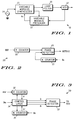
- PLL synthesizer 10 consists of a variable modulus prescaler 11 which divides the output frequency of a voltage controlled oscillator 12 to a predetermined frequency.
- a variable modulus synthesizer 13 is provided for dividing an output frequency of a reference oscillator 14 and a variable modulus prescaler 11; and comparing the divided reference output to the divided prescaler output in a phase comparator.
- the output of synthesizer 13 is then filtered in loop filter 15 and transmitted to VCO 12 to control the frequency/phase thereof.
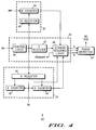
- Synthesizer 20 consists of an N (feedback) counter 21 which receives the feedback signal from the VCO, generally through a prescaler.
- Synthesizer 20 also consists of an R (reference) counter 22 which receives a reference signal. The outputs of the R and N counters, are transmitted to a phase detector 23 where they are compared. If the signals are out of phase, a corrective output signal is transmitted from phase detector 23 to the VCO.
- synthesizer 30 In addition to having an N (feedback) counter 31, an R (reference) counter 32, and a phase detector 33, synthesizer 30 also comprises a control logic circuit 34.
- logic control 34 is coupled to counters 31 and 32 to pass the data used to preset the counters and to synchronize the counters when terminating standby.
- Logic 34 is also coupled to phase detector 33 to control its output functions and its input signals when terminating standby.
- control logic 34 When in a standby mode, control logic 34 will inhibit the clock inputs to counters 31 and 32; shut down one or both of their input buffer amplifiers; and shut down phase detector 33 thereby conserving battery power.
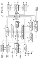
- a reference signal is provided to R counter 32 which is comprised of an R counter 44 and a R register 45.
- the R register 45 is used to retain the preset data input to synthesizer 30 through a control logic circuit 46.
- Control logic 46 also provides preset data to N counter 31.
- N counter 31 consists of an A counter 42, an N counter 43, and an A register 41 for storing the preset data from logic 46.
- Control logic 34 also contains a C register 47.
- C register 47 is provided with data to control several functions of synthesizer 30 including the standby mode. This will be discussed in more detail below.
- the C register provides a control output to a standby sequence logic 48.
- the standby sequence logic provides reference (f r ) and feedback (f v ) signals and a control output to phase detector 33 and also provides a standby signal to other system functions.
- phase detector 33 When the standby bit of C register 47 is set, the operation of phase detector 33 is inhibited. In addition, the standby signal acts to inhibit the Ref and f in signals to their respective counters.
- a reference buffer 51 has been added to receive the REF in signal from an oscillator.
- Buffer 51 has a control input from standby sequence logic 48 and a control input form a reference control 52.
- the reference signal from buffer 51 may be provided to both R counter 44 and reference control 52.
- Reference control 52 operates to provide reference output signal (REF out ). This signal may be adjusted according to a control signal from R register 45.
- the f in input from the prescaler is provided to an input amplifier 53 before being passed to counters 42 and 43.
- the amplified f in signal is also passed to standby logic 48 to be used in the process of terminating standby.
- Amp 53 also has a control input from standby sequence logic 48.
- Outputs from counters 42 and 43 are provided to a modulus control logic circuit 54 which has an output used to control the prescaler counter.
- Modulus control logic 54 also has a control input provided by standby sequence logic 48.
- Synthesizer 30 of FIG. 5 also contains a pair of phase detectors, phase detector A (33) and phase detector B (33').
- Phase detector A (33) receives inputs f r and f v from counters 43 and 44 via standby sequence logic 48 and a control input directly from logic 48.
- the f r and f v inputs are compared in detector 33 and a PD out phase correction signal is provided.
- Detector 33 also provides an output to detector 33' which also receives a control signal from logic 48.
- the outputs of detector 33' are phase and frequency signals ( ⁇ R and ⁇ V) derived from f r and f v .
- Synthesizer 30 also contains a lock detector 55 which receives an input from detector 33 and standby sequence logic 48. Lock detector 55 provides an LD signal which indicates when the f r and f v signals are in phase, locked.
- the C register (47) is the configuration register and may contain various bits for general control as well as bits related to the present invention. The bits relative to the present invention are designated C4 and C5.
- the configuration register is defined as follows: C7 C6 C5 C4 C3 C2 C1 C0 --- --- LDE STBY --- --- --- --- where: LDE enables/disables the lock detector when not in standby; and forces the LD output to a static high or a static low level when in standby; and STBY places the synthesizer in standby mode or terminates standby mode.
- a pull down termination resistor 60 having a first terminal connected to a signal line conducting signal f in , and a second terminal connected to a negative power supply voltage terminal designated "V SS ". While in standby, the current, R x , established by an external resistor is shut off; the bias establishing means to amplifier 53 and a pull down termination at f in are broken; and amp 53 gates off the f in signal. This results in a capacitive load being provided at the f in input. A capacitive load is provided to reduce prescaler power consumption since the prescaler may be external to the synthesizer and may not be placed in standby.
- R register 45 bits R15, R14, and R13
- OSC out static st.
- the recovery sequence is accomplished in two steps following the receipt at register C of a terminate standby signal.
- the f in bias establishing means and pull down termination are reconnected; amp 53 is gated on; and the Rx current is enabled.
- the output of buffer 51 is enabled to R counter 44 and, if buffer 51 has been inhibited, it is also enabled.
- the clock inputs to counters 42, 43, and 44 are enabled and the counters begin counting.
- any f r ' and f v ' signals are inhibited from toggling phase detectors 33 and 33' or lock detect 55 by standby sequence logic 48.
- the system awaits the first f v ' pulse to arrive from counter 43, indicating that counter 43 has completed a cycle.
- counter 44 is "jam" loaded with the preset stored in register 45 and the phase and lock detectors (33, 33', and 55) are initialized.
- the jam load synchronizes counters 42, 43, and 44 and creates outputs f r and f v to detector 33 that are in phase and represent the locked VCO condition (no error signal) that existed just prior to going into standby.
- the detectors are activated, but their outputs are still inhibited.
- the outputs are enabled upon the receipt, at standby sequence logic 48, of the first amplified f in signal following the first f v ' signal. This places the detectors in a state such that the next detector output signal is a true representation of any phase difference between the two input signals f r and f v .
- detector 33 were permitted to start operation without being initialized, the result could be a reversed interpretation of the lead/lag phase relation between f r and f v and the creation of erroneous polarity error signals when first exiting from standby, thus extending the time to acquire lock.
- the f v ' signal is used to commence phase two of the recovery from standby since the counting of the variable modulus prescaler is not controlled by the standby operation of the synthesizer.
- normal operation of the synthesizer is such that an f v ' signal is only generated at the completion of a prescaler count sequence (but not at the completion of every prescaler count sequence).
- f v ' represents a known position of the variable modulus prescaler.
- f v ' via standby sequence logic 48 and modulus control logic 54, is used to generate a modulus control signal to the prescaler to cause the prescaler to start a new, known, sequence of divide values. This new divide sequence is determined by the data preset into counters 42 and 43.
- a synthesizer has been shown which provides a device and method of standby which saves battery power and avoids delays in reestablishing a signal lock. Additionally, it has been shown that this is accomplished even when a variable modulus prescaler (outside direct control of the standby signal) is employed. Further, it has been shown that, when in standby mode, the standby method provides for control of output lock detect, modulus control, and reference signals; provides capacitive loads for the master reference frequency and prescaler input signals; and that the standby means is accomplished without requiring additional interface connections or power supply line switching to the synthesizer.
Landscapes
- Stabilization Of Oscillater, Synchronisation, Frequency Synthesizers (AREA)
Applications Claiming Priority (2)
| Application Number | Priority Date | Filing Date | Title |
|---|---|---|---|
| US07/633,867 US5075638A (en) | 1990-12-26 | 1990-12-26 | Standby system for a frequency synthesizer |
| US633867 | 1990-12-26 |
Publications (3)
| Publication Number | Publication Date |
|---|---|
| EP0492433A2 true EP0492433A2 (de) | 1992-07-01 |
| EP0492433A3 EP0492433A3 (en) | 1993-05-05 |
| EP0492433B1 EP0492433B1 (de) | 1999-03-17 |
Family
ID=24541446
Family Applications (1)
| Application Number | Title | Priority Date | Filing Date |
|---|---|---|---|
| EP91121780A Expired - Lifetime EP0492433B1 (de) | 1990-12-26 | 1991-12-19 | Verfahren und Vorrichtung zur Umschaltung eines Frequenzsynthesierers in einen Wartezustand |
Country Status (4)
| Country | Link |
|---|---|
| US (1) | US5075638A (de) |
| EP (1) | EP0492433B1 (de) |
| JP (1) | JP2841989B2 (de) |
| DE (1) | DE69131003T2 (de) |
Cited By (2)
| Publication number | Priority date | Publication date | Assignee | Title |
|---|---|---|---|---|
| US5471187A (en) * | 1993-03-10 | 1995-11-28 | National Semiconductor Corporation | Data signal comparation with self-adjusting threshold |
| EP0620651A3 (en) * | 1993-04-12 | 1995-12-13 | Motorola Inc | Method and apparatus for standby recovery in a phase locked loop. |
Families Citing this family (6)
| Publication number | Priority date | Publication date | Assignee | Title |
|---|---|---|---|---|
| US5842029A (en) * | 1991-10-17 | 1998-11-24 | Intel Corporation | Method and apparatus for powering down an integrated circuit transparently and its phase locked loop |
| US5473767A (en) * | 1992-11-03 | 1995-12-05 | Intel Corporation | Method and apparatus for asynchronously stopping the clock in a processor |
| US6097933A (en) * | 1997-12-04 | 2000-08-01 | Glenayre Electronics, Inc. | Method and apparatus for conserving power in a pager |
| US7027796B1 (en) * | 2001-06-22 | 2006-04-11 | Rfmd Wpan, Inc. | Method and apparatus for automatic fast locking power conserving synthesizer |
| US7289830B2 (en) * | 2005-03-18 | 2007-10-30 | Lear Corporation | System and method for vehicle module wake up in response to communication activity |
| EP2041599B1 (de) * | 2006-07-13 | 2010-09-01 | Siemens Aktiengesellschaft | Radaranordnung |
Family Cites Families (7)
| Publication number | Priority date | Publication date | Assignee | Title |
|---|---|---|---|---|
| US4030045A (en) * | 1976-07-06 | 1977-06-14 | International Telephone And Telegraph Corporation | Digital double differential phase-locked loop |
| JPS641330A (en) * | 1987-06-24 | 1989-01-05 | Matsushita Electric Ind Co Ltd | Frequency synthesizer |
| GB2207309B (en) * | 1987-07-11 | 1992-05-13 | Plessey Co Plc | Frequency synthesiser with provision for standby mode |
| US5008629A (en) * | 1988-06-20 | 1991-04-16 | Matsushita Electric Industrial Co., Ltd. | Frequency synthesizer |
| JP2795323B2 (ja) * | 1989-06-14 | 1998-09-10 | 富士通株式会社 | 位相差検出回路 |
| US4968950A (en) * | 1989-12-18 | 1990-11-06 | Motorola, Inc. | PLL frequency synthesizer output control circuit |
| US4951005A (en) * | 1989-12-27 | 1990-08-21 | Motorola, Inc. | Phase locked loop with reduced frequency/phase lock time |
-
1990
- 1990-12-26 US US07/633,867 patent/US5075638A/en not_active Expired - Lifetime
-
1991
- 1991-12-19 DE DE69131003T patent/DE69131003T2/de not_active Expired - Fee Related
- 1991-12-19 EP EP91121780A patent/EP0492433B1/de not_active Expired - Lifetime
- 1991-12-25 JP JP3356631A patent/JP2841989B2/ja not_active Expired - Fee Related
Cited By (3)
| Publication number | Priority date | Publication date | Assignee | Title |
|---|---|---|---|---|
| US5471187A (en) * | 1993-03-10 | 1995-11-28 | National Semiconductor Corporation | Data signal comparation with self-adjusting threshold |
| US5515364A (en) * | 1993-03-10 | 1996-05-07 | National Semiconductor Corporation | Radio frequency telecommunications transceiver |
| EP0620651A3 (en) * | 1993-04-12 | 1995-12-13 | Motorola Inc | Method and apparatus for standby recovery in a phase locked loop. |
Also Published As
| Publication number | Publication date |
|---|---|
| EP0492433A3 (en) | 1993-05-05 |
| DE69131003D1 (de) | 1999-04-22 |
| DE69131003T2 (de) | 1999-10-07 |
| EP0492433B1 (de) | 1999-03-17 |
| JPH04343525A (ja) | 1992-11-30 |
| US5075638A (en) | 1991-12-24 |
| JP2841989B2 (ja) | 1998-12-24 |
Similar Documents
| Publication | Publication Date | Title |
|---|---|---|
| JP3253630B2 (ja) | 位相ロックループのための位相同期回路 | |
| EP0272938B1 (de) | Frequenzsynthetisierer | |
| US5424689A (en) | Filtering device for use in a phase locked loop controller | |
| US6879188B2 (en) | Semiconductor integrated circuit device | |
| EP0777333B1 (de) | Energiesparende Phasenregelkreisschaltung | |
| US4743864A (en) | Power saving intermittently operated phase locked loop | |
| WO1998020620A1 (en) | Method and apparatus for reducing standby current in communications equipment | |
| WO2002076009A1 (en) | Fractional-n frequency synthesizer with fractional compensation method | |
| US7027796B1 (en) | Method and apparatus for automatic fast locking power conserving synthesizer | |
| EP0492433B1 (de) | Verfahren und Vorrichtung zur Umschaltung eines Frequenzsynthesierers in einen Wartezustand | |
| JP3253631B2 (ja) | 位相同期ループのためのエラー抑圧回路およびそのための方法 | |
| JPH011330A (ja) | 周波数シンセサイザ | |
| JP3397193B2 (ja) | クロック生成装置 | |
| JPH10308667A (ja) | Pll周波数シンセサイザ | |
| MXPA99000767A (es) | Aparato de division de frecuencia de modulo dual de contador individual. | |
| US6469583B1 (en) | PLL control circuit for digital oscillation frequency control and control method adopted in the same | |
| EP0206247A2 (de) | Frequenzsynthesierer mit Phasenregelschleife | |
| US7103132B1 (en) | Phase comparator and method of controlling power saving operation of the same, and semiconductor integrated circuit | |
| EP0299674A2 (de) | Frequenzsynthesierer | |
| US6304147B1 (en) | Method and circuit for reduced power consumption in a charge pump circuit | |
| JPH0472413B2 (de) | ||
| JP3006805B2 (ja) | ダイレクトディジタルシンセサイザを用いた局部発振回路 | |
| JP2773481B2 (ja) | ダイレクトディジタルシンセサイザを用いた局部発振回路 | |
| JPH05304469A (ja) | Pll周波数シンセサイザ回路 | |
| KR20040022652A (ko) | 락킹 시간을 줄이기 위한 주파수 교정회로를 가지는pll 및 이를 이용한 락킹 방법 |
Legal Events
| Date | Code | Title | Description |
|---|---|---|---|
| PUAI | Public reference made under article 153(3) epc to a published international application that has entered the european phase |
Free format text: ORIGINAL CODE: 0009012 |
|
| AK | Designated contracting states |
Kind code of ref document: A2 Designated state(s): DE FR GB |
|
| PUAL | Search report despatched |
Free format text: ORIGINAL CODE: 0009013 |
|
| AK | Designated contracting states |
Kind code of ref document: A3 Designated state(s): DE FR GB |
|
| 17P | Request for examination filed |
Effective date: 19931102 |
|
| 17Q | First examination report despatched |
Effective date: 19940110 |
|
| GRAG | Despatch of communication of intention to grant |
Free format text: ORIGINAL CODE: EPIDOS AGRA |
|
| GRAG | Despatch of communication of intention to grant |
Free format text: ORIGINAL CODE: EPIDOS AGRA |
|
| GRAG | Despatch of communication of intention to grant |
Free format text: ORIGINAL CODE: EPIDOS AGRA |
|
| GRAH | Despatch of communication of intention to grant a patent |
Free format text: ORIGINAL CODE: EPIDOS IGRA |
|
| GRAH | Despatch of communication of intention to grant a patent |
Free format text: ORIGINAL CODE: EPIDOS IGRA |
|
| GRAA | (expected) grant |
Free format text: ORIGINAL CODE: 0009210 |
|
| AK | Designated contracting states |
Kind code of ref document: B1 Designated state(s): DE FR GB |
|
| REF | Corresponds to: |
Ref document number: 69131003 Country of ref document: DE Date of ref document: 19990422 |
|
| ET | Fr: translation filed | ||
| PLBE | No opposition filed within time limit |
Free format text: ORIGINAL CODE: 0009261 |
|
| STAA | Information on the status of an ep patent application or granted ep patent |
Free format text: STATUS: NO OPPOSITION FILED WITHIN TIME LIMIT |
|
| 26N | No opposition filed | ||
| REG | Reference to a national code |
Ref country code: GB Ref legal event code: IF02 |
|
| REG | Reference to a national code |
Ref country code: GB Ref legal event code: 732E |
|
| PGFP | Annual fee paid to national office [announced via postgrant information from national office to epo] |
Ref country code: GB Payment date: 20061106 Year of fee payment: 16 |
|
| PGFP | Annual fee paid to national office [announced via postgrant information from national office to epo] |
Ref country code: FR Payment date: 20061201 Year of fee payment: 16 |
|
| PGFP | Annual fee paid to national office [announced via postgrant information from national office to epo] |
Ref country code: DE Payment date: 20061229 Year of fee payment: 16 |
|
| GBPC | Gb: european patent ceased through non-payment of renewal fee |
Effective date: 20071219 |
|
| PG25 | Lapsed in a contracting state [announced via postgrant information from national office to epo] |
Ref country code: DE Free format text: LAPSE BECAUSE OF NON-PAYMENT OF DUE FEES Effective date: 20080701 |
|
| REG | Reference to a national code |
Ref country code: FR Ref legal event code: ST Effective date: 20081020 |
|
| PG25 | Lapsed in a contracting state [announced via postgrant information from national office to epo] |
Ref country code: GB Free format text: LAPSE BECAUSE OF NON-PAYMENT OF DUE FEES Effective date: 20071219 |
|
| PG25 | Lapsed in a contracting state [announced via postgrant information from national office to epo] |
Ref country code: FR Free format text: LAPSE BECAUSE OF NON-PAYMENT OF DUE FEES Effective date: 20071231 |