EP0492677B1 - Photoemissionselektronenstrahlmesssonde mit gepulstem Laser - Google Patents
Photoemissionselektronenstrahlmesssonde mit gepulstem Laser Download PDFInfo
- Publication number
- EP0492677B1 EP0492677B1 EP91202756A EP91202756A EP0492677B1 EP 0492677 B1 EP0492677 B1 EP 0492677B1 EP 91202756 A EP91202756 A EP 91202756A EP 91202756 A EP91202756 A EP 91202756A EP 0492677 B1 EP0492677 B1 EP 0492677B1
- Authority
- EP
- European Patent Office
- Prior art keywords
- electron
- laser
- test probe
- probe system
- photocathode
- Prior art date
- Legal status (The legal status is an assumption and is not a legal conclusion. Google has not performed a legal analysis and makes no representation as to the accuracy of the status listed.)
- Expired - Lifetime
Links
- 238000010894 electron beam technology Methods 0.000 title claims description 110
- 239000000523 sample Substances 0.000 title claims description 85
- 238000012360 testing method Methods 0.000 claims description 124
- 238000012545 processing Methods 0.000 claims description 30
- 238000005259 measurement Methods 0.000 claims description 29
- 230000003287 optical effect Effects 0.000 claims description 28
- 230000005540 biological transmission Effects 0.000 claims description 12
- 230000001360 synchronised effect Effects 0.000 claims description 12
- 238000000034 method Methods 0.000 claims description 10
- 239000010453 quartz Substances 0.000 claims description 7
- 230000004044 response Effects 0.000 claims description 7
- VYPSYNLAJGMNEJ-UHFFFAOYSA-N silicon dioxide Inorganic materials O=[Si]=O VYPSYNLAJGMNEJ-UHFFFAOYSA-N 0.000 claims description 7
- 239000003381 stabilizer Substances 0.000 claims description 7
- 239000000758 substrate Substances 0.000 claims description 7
- 238000013461 design Methods 0.000 claims description 5
- 239000013307 optical fiber Substances 0.000 claims description 5
- WUKWITHWXAAZEY-UHFFFAOYSA-L calcium difluoride Chemical compound [F-].[F-].[Ca+2] WUKWITHWXAAZEY-UHFFFAOYSA-L 0.000 claims description 4
- 229910001634 calcium fluoride Inorganic materials 0.000 claims description 4
- PCHJSUWPFVWCPO-UHFFFAOYSA-N gold Chemical compound [Au] PCHJSUWPFVWCPO-UHFFFAOYSA-N 0.000 claims description 4
- 229910052737 gold Inorganic materials 0.000 claims description 4
- 239000010931 gold Substances 0.000 claims description 4
- 230000001419 dependent effect Effects 0.000 claims description 3
- 230000000694 effects Effects 0.000 claims description 3
- 230000008569 process Effects 0.000 claims description 3
- 238000004458 analytical method Methods 0.000 claims description 2
- 238000007789 sealing Methods 0.000 claims 2
- 230000008878 coupling Effects 0.000 claims 1
- 238000010168 coupling process Methods 0.000 claims 1
- 238000005859 coupling reaction Methods 0.000 claims 1
- 230000001131 transforming effect Effects 0.000 claims 1
- 239000013598 vector Substances 0.000 description 18
- 238000010586 diagram Methods 0.000 description 13
- 238000005070 sampling Methods 0.000 description 12
- 239000013078 crystal Substances 0.000 description 9
- 230000003111 delayed effect Effects 0.000 description 7
- 229910001218 Gallium arsenide Inorganic materials 0.000 description 5
- 239000004020 conductor Substances 0.000 description 5
- 239000012212 insulator Substances 0.000 description 4
- 230000000630 rising effect Effects 0.000 description 4
- 230000007704 transition Effects 0.000 description 4
- 238000005516 engineering process Methods 0.000 description 3
- 239000000835 fiber Substances 0.000 description 3
- 238000012986 modification Methods 0.000 description 3
- 230000004048 modification Effects 0.000 description 3
- 230000001960 triggered effect Effects 0.000 description 3
- XBJJRSFLZVLCSE-UHFFFAOYSA-N barium(2+);diborate Chemical compound [Ba+2].[Ba+2].[Ba+2].[O-]B([O-])[O-].[O-]B([O-])[O-] XBJJRSFLZVLCSE-UHFFFAOYSA-N 0.000 description 2
- 230000033228 biological regulation Effects 0.000 description 2
- 238000003745 diagnosis Methods 0.000 description 2
- 230000010354 integration Effects 0.000 description 2
- 239000000463 material Substances 0.000 description 2
- 230000010363 phase shift Effects 0.000 description 2
- 230000000717 retained effect Effects 0.000 description 2
- 238000004626 scanning electron microscopy Methods 0.000 description 2
- 125000003821 2-(trimethylsilyl)ethoxymethyl group Chemical group [H]C([H])([H])[Si](C([H])([H])[H])(C([H])([H])[H])C([H])([H])C(OC([H])([H])[*])([H])[H] 0.000 description 1
- RYGMFSIKBFXOCR-UHFFFAOYSA-N Copper Chemical compound [Cu] RYGMFSIKBFXOCR-UHFFFAOYSA-N 0.000 description 1
- 239000004642 Polyimide Substances 0.000 description 1
- XUIMIQQOPSSXEZ-UHFFFAOYSA-N Silicon Chemical compound [Si] XUIMIQQOPSSXEZ-UHFFFAOYSA-N 0.000 description 1
- PNEYBMLMFCGWSK-UHFFFAOYSA-N aluminium oxide Inorganic materials [O-2].[O-2].[O-2].[Al+3].[Al+3] PNEYBMLMFCGWSK-UHFFFAOYSA-N 0.000 description 1
- 238000010420 art technique Methods 0.000 description 1
- 230000008901 benefit Effects 0.000 description 1
- 230000015556 catabolic process Effects 0.000 description 1
- 239000000919 ceramic Substances 0.000 description 1
- 230000008859 change Effects 0.000 description 1
- 238000012512 characterization method Methods 0.000 description 1
- 230000006835 compression Effects 0.000 description 1
- 238000007906 compression Methods 0.000 description 1
- 238000010276 construction Methods 0.000 description 1
- 238000011109 contamination Methods 0.000 description 1
- 238000007796 conventional method Methods 0.000 description 1
- 238000001816 cooling Methods 0.000 description 1
- 229910052802 copper Inorganic materials 0.000 description 1
- 239000010949 copper Substances 0.000 description 1
- 238000012937 correction Methods 0.000 description 1
- 230000003247 decreasing effect Effects 0.000 description 1
- 238000006731 degradation reaction Methods 0.000 description 1
- 230000001934 delay Effects 0.000 description 1
- 238000000151 deposition Methods 0.000 description 1
- 238000011161 development Methods 0.000 description 1
- 239000000428 dust Substances 0.000 description 1
- 229920001971 elastomer Polymers 0.000 description 1
- 239000000806 elastomer Substances 0.000 description 1
- 238000000605 extraction Methods 0.000 description 1
- 230000002452 interceptive effect Effects 0.000 description 1
- 229910052746 lanthanum Inorganic materials 0.000 description 1
- FZLIPJUXYLNCLC-UHFFFAOYSA-N lanthanum atom Chemical compound [La] FZLIPJUXYLNCLC-UHFFFAOYSA-N 0.000 description 1
- HIQSCMNRKRMPJT-UHFFFAOYSA-J lithium;yttrium(3+);tetrafluoride Chemical compound [Li+].[F-].[F-].[F-].[F-].[Y+3] HIQSCMNRKRMPJT-UHFFFAOYSA-J 0.000 description 1
- 238000003754 machining Methods 0.000 description 1
- 238000000691 measurement method Methods 0.000 description 1
- 230000007246 mechanism Effects 0.000 description 1
- 238000004377 microelectronic Methods 0.000 description 1
- 230000005693 optoelectronics Effects 0.000 description 1
- 238000004806 packaging method and process Methods 0.000 description 1
- 229920001721 polyimide Polymers 0.000 description 1
- WYOHGPUPVHHUGO-UHFFFAOYSA-K potassium;oxygen(2-);titanium(4+);phosphate Chemical compound [O-2].[K+].[Ti+4].[O-]P([O-])([O-])=O WYOHGPUPVHHUGO-UHFFFAOYSA-K 0.000 description 1
- 238000012827 research and development Methods 0.000 description 1
- 229910052710 silicon Inorganic materials 0.000 description 1
- 239000010703 silicon Substances 0.000 description 1
- 238000004088 simulation Methods 0.000 description 1
- 239000007787 solid Substances 0.000 description 1
- 238000001228 spectrum Methods 0.000 description 1
- 230000007480 spreading Effects 0.000 description 1
- 238000003892 spreading Methods 0.000 description 1
- 230000006641 stabilisation Effects 0.000 description 1
- 238000011105 stabilization Methods 0.000 description 1
- 230000000153 supplemental effect Effects 0.000 description 1
- VLCQZHSMCYCDJL-UHFFFAOYSA-N tribenuron methyl Chemical compound COC(=O)C1=CC=CC=C1S(=O)(=O)NC(=O)N(C)C1=NC(C)=NC(OC)=N1 VLCQZHSMCYCDJL-UHFFFAOYSA-N 0.000 description 1
- WFKWXMTUELFFGS-UHFFFAOYSA-N tungsten Chemical compound [W] WFKWXMTUELFFGS-UHFFFAOYSA-N 0.000 description 1
- 229910052721 tungsten Inorganic materials 0.000 description 1
- 239000010937 tungsten Substances 0.000 description 1
- 238000012795 verification Methods 0.000 description 1
- 229910000859 α-Fe Inorganic materials 0.000 description 1
Images


Classifications
-
- G—PHYSICS
- G01—MEASURING; TESTING
- G01R—MEASURING ELECTRIC VARIABLES; MEASURING MAGNETIC VARIABLES
- G01R31/00—Arrangements for testing electric properties; Arrangements for locating electric faults; Arrangements for electrical testing characterised by what is being tested not provided for elsewhere
- G01R31/28—Testing of electronic circuits, e.g. by signal tracer
- G01R31/317—Testing of digital circuits
- G01R31/3181—Functional testing
- G01R31/319—Tester hardware, i.e. output processing circuits
- G01R31/31917—Stimuli generation or application of test patterns to the device under test [DUT]
- G01R31/31922—Timing generation or clock distribution
-
- G—PHYSICS
- G01—MEASURING; TESTING
- G01R—MEASURING ELECTRIC VARIABLES; MEASURING MAGNETIC VARIABLES
- G01R31/00—Arrangements for testing electric properties; Arrangements for locating electric faults; Arrangements for electrical testing characterised by what is being tested not provided for elsewhere
- G01R31/28—Testing of electronic circuits, e.g. by signal tracer
- G01R31/302—Contactless testing
- G01R31/305—Contactless testing using electron beams
Definitions
- the present invention relates to electron-beam probing methods and systems useful, for example, in analyzing operation of Very Large Scale Integrated (VLSI) circuit devices.
- the present invention relates to electron-beam probing methods and systems in which test patterns generated to exercise a device are synchronized with pulsed-laser photoemission of an electron probe beam.
- VLSI circuit devices Characterizing and verifying the operation of VLSI circuit devices is an important element of their design. Probing internal nodes of such devices plays an increasingly significant role in this process.
- E-beam probing uses the principle of voltage contrast in a scanning electron microscope (SEM) to perform VLSI diagnosis through non-contact electron-beam measurement of internal signals in a VLSI device.
- SEM scanning electron microscope
- a focused beam of primary electrons is directed toward a conductor within a circuit specimen as signals are applied to the specimen.
- Detected secondary electrons are indicative of the surface electrical potential on conductors within the specimen. See, for example, E. Menzel & E. Kubalek, Fundamentals of Electron Beam Testing of Integrated Circuits, 5 SCANNING 103-122 (1983), and E. Plies & J. Otto, Voltage Measurement Inside Integrated Circuit Using Mechanical and Electron Probes, IV SCANNING ELECTRON MICROSCOPY 1491-1500 (1985).
- Richardson IDS 5000 an Integrated Diagnosis System for VLSI , 7 MICROELECTRONIC ENGINEERING (1987); and see U.S. Patents 4,706,019 and 4,721,909 to N. Richardson. See also J. FROSIEN, et al., High Performance Electron Optical Column for Testing ICs with Submicrometer Design Rules, MICROELECTRON. ENG. (NETHERLANDS), vol. 7., no. 2-4, pp. 163-72 (First European Conference on Electron and Optical Beam Testing of Integrated Circuits, Grenoble, France, 9-11 December 1987).
- FIG. 1 is a block diagram of a prior art electron-beam test probe system 110.
- the system has three main functional elements: an electron-beam test probe 112, a circuit exerciser 114, and a data processing system 116 which includes a display terminal 118.
- the circuit exerciser 114 may be a conventional integrated circuit tester, such as a model "S 15TM” tester available from Schlumberger Technologies of San Jose, California, which can repeatedly apply a pattern of test vectors to the specimen circuit over a bus 124.
- the specimen circuit (device under test, or DUT) 126 is placed in a vacuum chamber 128 of the electron-beam test probe 112 so that potential measurements can be made as the test vector pattern is applied.
- the points at which such measurements are to be made are sent to the electron-beam test probe 112 by the data processing system 116 over a bus 122.
- the data processing system 116 may also be used to specify the test signal pattern used and the timing of the potential measurements relative to the test signal pattern.
- the electron-beam test probe system is controlled by an operator who inputs commands through the display terminal 118.
- SEMs used for electron-beam probing such as that in the IDS 5000 system, are equipped with high-speed beam pulsing hardware sometimes referred to as a "beam-blanker.”
- An example of such hardware is described in U.S. Patent 4,721,909. Directing a pulsed electron beam at a particular node of interest provides a mode of operation much like that of a sampling oscilloscope, in which images can be produced of waveforms at one or more nodes in the specimen circuit as test vector patterns are applied to the specimen circuit.
- a measurement is made by pulsing the electron beam at a specific time during application of the test vector pattern to the specimen circuit. Since the time needed to make a potential measurement is generally longer than the time over which the test signal pattern remains constant, stroboscopic techniques are used. That is, the electron beam is turned on for a brief period of time at a point in the test signal pattern. Each time the electron beam is so pulsed, a measurement of the potential on a node of the specimen circuit is made.
- the electron source brightness obtained with the conventionally-used tungsten or lanthanum hexaboride thermionic emitters is low; at the necessarily low beam accelerating voltage of around 1 kV, the amount of peak current in the final electron probe is limited to about 1 nA when the probe diameter is around 0.1 micron.
- the beam is pulsed with a duration of less than 50 ps (picoseconds) in order to perform high speed sampling measurements, the statistical average number of electrons per pulse is less than one.
- the duty cycle the trigger period divided by the beam pulse width
- leakage currents and other measurement limitations result in degraded measurement accuracy.
- Data acquisition time is a real concern, particularly with the lengthy test vector patterns require to exercise ever more complex integrated circuits.
- pulsed-laser photoemission source offers a dramatically brighter source of short-duration electron-beam pulses (on the order of 10 1 electrons per pulse vs. 10 -2 electrons per pulse with typical thermionic sources)
- the pulsed-laser electron-beam cannot be readily turned on and off in response to trigger pulses from the test pattern generator in the manner employed with thermionic sources.
- the phase of the pulsed-laser electron-beam be readily shifted with respect to a fixed time reference.
- matching the electron-beam pulses to the test pattern from the circuit exerciser by controlling the electron-beam source does not appear feasible with a pulsed-laser photoemission source.
- the waveform is a single pulse photoconductively launched on a transmission line.
- the waveform is a square-wave signal triggered by applying the laser to a photodiode.
- the phase variation is no more than one period of the probing frequency because it is generated by varying the path length of the optical trigger for the electrical waveform on the DUT.
- EP-A-0 357 440 discloses an electro-optic test system having as an optical sampling source a mode-locked laser which generates light pulses at a constant repetition rate.
- the light output is split.
- One beam is incident on a photodetector, the electronic signal output of which drives a counter.
- the counter output provides a phase reference signal for a time base frequency synthesizer.
- the counter output is also used as a timing signal for an optical pulse selector which gates the optical output pulses of the laser and passes only those optical pulses which are time coincident with the output pulses of the counter. Those optical pulses which pass become the optical sampling pulses for sampling a DUT.
- a further problem is raised by the fact that switching times of elements within the device under test (DUT) can be below 10 ps, yet conventional techniques of connecting to the device do not allow signals with transition times much below 50 ps to be effectively coupled into or out of the device.
- DUT device under test
- a complex component is made by interconnecting thousands of active elements together on a chip. What is of interest is the actual performance of elements internal to the device.
- the non-contact, high-bandwidth measurement technique of electron-beam probing allows detailed observation of the timing relationships of signals internal to the device.
- each device connection e.g., bond wire, probe pin and even bond pad
- each device connection represents an unknown, complex impedance between the stimulus source and the on-chip element.
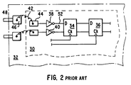
- Figure 2 shows schematically a portion of a VLSI circuit device 30 mounted on a carrier 32.
- Active elements forming part of device 30 include flip-flops 34 and 36 and inverters 38 and 40.
- Each of flip-flops 34 and 36 has a data input port D and a clock input port Ck.
- Bond wire 42 electrically connects bond pad 44 of device 30 to bond pad 46 of carrier 32.
- Bond pad 46 is in turn electrically connected to an input pin 48.
- Circuit exerciser 114 causes the electron-beam probe to be pulsed in stroboscopic fashion by sending trigger pulses (as shown in line "a" of Figure 3) to the test probe 112. Test patterns produced by circuit exerciser 114 are synchronized with these trigger pulses.
- circuit exerciser 114 may be capable of generating a test pattern having a rising edge of, say, 10 ps duration as shown in line "b" of Figure 3, the impedance encountered over the path from input pin 48 to the active element 34 to be examined acts as a low-pass filter and introduces some indeterminate delay. That is, the rise time of the pulse at input port 50 of active element 38 may have a duration of, say, 50 ps as shown in line "c" of Figure 3. While on-chip element 38 may be able to restore the rise time of the pulse at input port 52 of element 34 to 10 ps as shown in line "d” of Figure 3, the intended placement of the rising edge is no longer assured.
- an electron-beam test probe system 400 for analyzing an electronic circuit, the analysis including the measurement of the potential at selected points on the electronic circuit, the electron-beam test probe system comprising:
- an electron beam is used not only as a high-bandwidth, guided probe for interactive waveform measurement but also as a tester (circuit exerciser) calibration probe.
- the test pattern applied to the external pins of the DUT can be adjusted ( e.g., time-shifted) while the actual signal at a port of an element of interest (e.g., an active element such as a flip-flop on the DUT) is observed.
- test pattern edges may be placed with precision of a few picoseconds (ps) at each port of an element of interest, before further measurements are made within the DUT.
- the present invention is directed to implementation of a practical electron beam probing system with a time resolution on the order of 10 ps, together with a low-jitter, high-accuracy test pattern source with multiple output pins and flexible formatting capability.
- the basic architecture of the Schlumberger IDS 5000 electron beam diagnostic system is retained to provide a convenient user interface and convenient access to the electronic circuit under test. Significant modifications made, however, are described below.
- FIG. 4 is a schematic block diagram of a preferred embodiment of an electron-beam system 400 in accordance with the present invention.
- System 400 comprises a test probe 402, a laser subsystem 404 with associated power supply and cooling unit 406, an optical coupler 452 (such as a light pipe or optical fiber), a reference oscillator 408, a phase stabilizer 410, a timebase circuit 412, a pulse-picker circuit 414, a test pattern generator 416, a set of controlled-impedance transmission lines 454, a data-processing system 418, and a display terminal 420.
- Test probe 402 comprises a wafer stage 422 for holding and positioning a wafer bearing one or more IC devices to be probed, wafer probes 424, an electron-beam column 426, an electron-beam blanker 428 ( e.g., of the type described in U.S. Patent 4,721,909), and a photocathode assembly 430.
- Laser subsystem 404 includes a mode locker 434 and a phase monitor 432, among other elements which will be described below.
- Timebase circuit 412 comprises a sine-to-ECL converter 436, a hold-off delay 438, a fine-delay phase-locked loop 440, and a coarse delay counter 442.
- Test pattern generator circuit 416 comprises a set of timing generators 444, a set of formatters 446, and a set of pin drivers 448.
- Data processing system 418 communicates with each of the system elements via control and data lines 450 which may, for example, be in the form of one or more serial and/or parallel data buses.
- reference oscillator 408 produces a 120 MHz sine wave reference signal which is supplied to phase stabilizer 410 and to timebase circuit 412.
- phase stabilizer 410 in turn supplies a 120 MHz sine wave drive signal to mode locker 434 of laser subsystem 404.
- Phase monitor 432 provides a feedback signal to phase stabilizer 410 to assure stabilization of the output pulse train of laser subsystem 404.
- Laser subsystem 404 generates a train of ultraviolet (UV) wavelength laser pulses at a repetition frequency of 240 MHz, the laser pulses being conveyed via an optical coupler (light pipe or optical fiber) 452 to photocathode assembly 430 of test probe 402.
- UV ultraviolet
- Photocathode assembly 402 produces an electron-beam pulse in response to each laser pulse arriving through light pipe or optical fiber 452.
- the electron-beam pulses may be directed to "probe" the DUT and supply signals to data processing system 418 which may be used to display measured parameters of the DUT on display terminal 420.
- Timebase circuit 412 serves to synchronize the test pattern applied to a DUT (mounted in test probe 402) with electron-beam pulses applied to the DUT. Electron-beam pulses to be applied to the DUT are selected by unblanking of the electron-beam pulse train under control of pulse picker 414 and hold-off delay 438, hold-off delay 438 being supplied with the 120 MHz reference signal via sine-to-ECL converter 436.
- a test pattern to be applied to the DUT may be controllably time-shifted relative to the electron-beam pulse train by means of the fine-delay phase-locked loop 440 and coarse-delay counter 442.
- a desired pattern of test vectors to be applied to the DUT is generated by means of timing generators 444 and formatters 446, and supplied to the DUT via pin drivers 448, controlled-impedance transmission lines 454, and wafer probes 424.
- the test-vector pattern may be time-shifted relative to the laser/e-beam pulses by control of timebase circuit 412.
- the time shift imposed by timebase circuit 412 is controlled by data processing system 418 via control and data lines 450.
- Test pattern edges at conductors of interest within the DUT may thus be controllably time-positioned relative to the electron-beam probe pulses applied to those conductors.
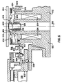
- FIG. 5 is a schematic, sectional view of the test probe of Figure 4.
- Wafer stage 422 comprises a chuck 502 for holding a wafer 504 within a vacuum chamber 506, and an X stage 510, a Y stage 512, a Z stage 514 and a Theta stage 516 for positioning chuck 502 and wafer 504 relative to wafer probes 424.
- a positioning stage is described in U.S. Patent No. 4,706,019 and provided, for example, in the commercially-available Schlumberger IDS 5000 system.
- Wafer stage 422 is mounted on a base plate 518 which is supported on vibration isolators 520.
- Electron-beam column 426 comprises an electrostatic lens assembly 523, a condenser lens 524, an objective lens 526, an energy analyzer electrode 528, an extractor electrode 529, an electron detector 530, an X stage 532 and a Y stage 534 mounted on supports 536.
- a sliding vacuum seal 538 allows electron-beam column 426 to be moved relative to wafer 504 by means of X,Y stages 532 and 534 without loss of vacuum in chamber 506.
- well-known elements of the test probe are not illustrated in Figure 5, such as control and signal and power lines to and from the stages, lenses and electron detector.
- the circuit device under test (e.g., on wafer 504) is placed in vacuum chamber 506, which is evacuated by means of a pump (not illustrated).
- a pump not illustrated
- an adapter comprising a printed circuit board and device socket are used to connect the pins of the DUT to incoming test patterns from the circuit exerciser, in conventional fashion.
- high-bandwidth co-planar waveguide wafer probe pins may be used to deliver the incoming test patterns (e.g., WPH 700 series, available from Cascade Microtech, of Beaverton, Oregon).
- Transmission lines 454 may be individual coaxial cables or may be microstrip fabricated by depositing copper traces on a flexible substrate such as polyimide. Microstrip transmission lines are also available from Cascade Microtech.
- Figure 6 is a partial, sectional, schematic view showing in greater detail the wafer probes and portions of the electron-beam column of Figure 4.
- a support member 602 into which is fitted a probe carrier 604.
- Wafer probes 424 are mounted on mode suppressors 606 (of a lossy, ferrite material), which are in turn mounted on probe carrier 604. Adjusting screws (not shown) facilitate alignment of the wafer probe tips in the plane of a wafer 504 to be probed.
- Signals from pin drivers 448 are conveyed to wafer probes 424 by coaxial cables (not shown) via SMA-type connectors 608 and flexible microstrip transmission lines 610 (shown as dashed lines).
- the upper end of column 426 includes an objective lens body 612, an objective lens coil 614, extractor electrode 529 (which may include a mesh, not shown), and deflection coils 616 (for scanning and/or vectoring the electron beam).
- the electron-optical axis of the body 612 is indicated by dashed line 618.
- Body 612 is laterally movable relative to base plate 518 and support member 602 by means of stages 532 and 534, for aiming the electron-beam probe at a desired location on wafer 504. Seal 538 allows such movement without loss of vacuum in chamber 506.
- Shown at the left side of axis 612 is a mode suppressor 606 which has been modified to allow room for the upper end of body 612 and electrode 529.
- Shown at the right side of axis 612 is a mode suppressor 606 which has not been so modified; phantom lines indicate the region of where mode suppressor end portion 620 may interfere with body 612 and electrode 529. It is the end portion 620 which is preferably removed (as mentioned above) to avoid such interference.
- the layout of pulsed-laser sub-system 404 of Figure 4 is shown in schematic plan view in Figure 7.
- a flash-lamp-pumped, short-cavity, mode-locked, Neodymium-YLF (Yttrium-Lithium-Fluoride) laser produces pulses of 25 ps duration, about 4W average power, at 1053 nm in the infra-red (IR) frequency range.
- the first stage comprises a high-resolution mirror assembly 704, a cavity length adjuster 706, an intra-cavity shutter 708, a laser head 710 having a pump lamp 712 and a laser medium 714, an aperture 716, mode locker 434, and an output mirror 718.
- Beam turning mirrors 720 and 722 pass the pulsed IR laser beam to the second stage, and allow the beam to be sampled by phase monitor 432 via a right-angle prism 724 and by an IR amplitude monitor 726.
- a feedback signal output from phase monitor 432 is supplied to phase stabilizer 410 as shown in Figure 4.
- the second stage of laser subsystem 404 comprises a second-harmonic generator 728 which preferably includes a KTP (potassium titanyl phosphate) frequency-doubler crystal which converts the incoming IR pulses to shorter duration pulses (e.g., pulses of 25/ ⁇ 2 ps duration) in the green part of the spectrum (e.g., at 527 nm wavelength) at much lower power ( e.g., a few hundred milliwatts).
- the second stage further comprises beam-turning mirrors 730 and 732, the latter permitting sampling of the green laser pulses by a 527 nm power monitor 736.
- the green output beam from the second stage is fed to a fourth-harmonic generator 734 of the third stage.
- Fourth-harmonic generator 734 includes a final doubler crystal (for example, of beta barium borate (BBO) or KDP crystals) which converts the green pulses from the second stage into pulses of about 12 ps duration at 263 nm in the ultra-violet (UV) range at still lower power ( e.g., a few milliwatts).
- the third stage further comprises beam-turning mirrors 738 and 740, and a 263 nm power monitor 744.
- the final stage of the laser sub-system includes beam focusing optics 742 which pass the UV laser pulses to optical coupler 452.
- Optical coupler 452 is preferably a light pipe (e.g., produced by Laser Mechanisms of Southfield, Michigan, and available through Quantronix Corporation of Smithtown, New York) comprising a flexible or articulated tube having knuckle joints fitted with mirrors to convey the pulsed UV beam to photocathode 430, though other suitable means such as a single-mode UV fiber or the like may be used.
- IR amplitude monitor 726 is used for internal regulation of laser subsystem 404, as are the outputs of power monitors 736 and 744.
- the frequency doubler crystals of generators 728 and 734 must be temperature-controlled.
- the internal regulation means of laser subsystem 404 is not illustrated, for simplicity of description.
- a flash-lamp-pumped, short-cavity, mode-locked, Neodymium-YLF laser of the type described is commercially available from Quantronix Corporation of Smithtown, New York, Model 498MLSHFH-240.
- the described laser subsystem provides a highly-stable source of narrow UV pulses (e.g., having a pulse width on the order of 12 ps) at a repetition frequency of, for example, 240 MHz.
- Other suitable laser sources may be used, if desired.
- a long-cavity YAG laser was used, which gives fairly broad pulses on the order of 70 ps, and employs a fiber grating compressor. It requires that the beam be launched into a fiber, and tends to be difficult to handle.
- the flash-lamp-pumped, short-cavity, mode-locked, Neodymium-YLF laser described above with reference to Figure 7 is expected to be somewhat less performant (e.g., 12 ps pulse width vs. 2 ps pulse width), but is preferred as it currently appears to offer the greater durability and stability desired for a commercial system.
- laser subsystem Numerous other modifications to the laser subsystem are also possible. For example, it may be possible to mount harmonic generator 734 onto photocathode assembly 430, and to employ a flexible optical coupler to convey green laser light from generator 728 to generator 734. Similarly, it may be possible to mount harmonic generators 728 and 724 onto photocathode assembly 430, and to employ a flexible optical coupler to convey infrared laser light from first stage 702 to harmonic generator 728. Also, it is envisioned that pump flash-lamp 712 may be replaced with solid-state, infrared diodes. In this case, it may be possible to mount substantially all of the laser subsystem onto photocathode assembly 430, which is affixed to and moves with column 426.
- FIG. 8 is a cross-sectional view of a portion of test probe 402 showing principal elements of photocathode assembly 430 and certain surrounding components.
- Ultraviolet laser pulses arriving via optical coupler 452 pass through a focusing lens 802 to a photocathode element 804 which produces an electron-beam pulse in response to each laser pulse.
- the electron-beam pulses pass through an aperture in an extractor anode 806 of electron-beam column 426.
- Anode 806 is preferably maintained at a relatively high positive voltage (e.g., 3 kV - 4 kV) so as to accelerate the electrons sufficiently to avoid space-charge spreading of the electron-beam pulses.
- Photocathode element 804 preferably comprises a transparent, quartz disk of 3 mm thickness, optically polished on both faces to transmit UV laser light with minimum distortion, with a layer of calcium fluoride deposited on its upper surface and with a layer of gold deposited over the calcium fluoride layer.
- Photocathode assembly 430 is preferably designed to replace the thermionic electron-beam gun of a conventional IDS 5000TM test probe system.
- a generally-cylindrical main body 810 mounts on the lower end 812 of electron-beam column 426, and is held in place by a clamp 814.
- a conductive, photocathode carrier ring 816 held between column lower end 812 and a shoulder of main body 810 is a conductive, photocathode carrier ring 816.
- O-ring 818 hermetically seals the junction between column lower end 812 and carrier ring 816.
- An insulator ring 820 mounts within carrier ring 816, and a conductive photocathode support ring 822 mounts within insulator ring 820.
- carrier ring 816 and insulator ring 820, and between insulator ring 820 and support ring 822, are hermetically sealed by O-rings 824 and 826, respectively.
- Photocathode 804, which fits into support ring 822, is held in place by a conductive closure ring 826 which threads onto the lower end of support ring 822.
- An O-ring 828 hermetically seals the junction between photocathode 804 and support ring 822.
- photocathode 804 serves as a lower vacuum boundary of electron-beam column 426. That is, the region above photocathode 804 is contiguous with the evacuated column 426 and chamber 506, and the region below photocathode 804 contains air at atmospheric pressure.
- One or more screws 830 threaded into main body 810 serve to laterally position carrier ring 816.
- the photocathode may be refreshed from time to time by turning screws 830 to laterally displace carrier ring 816.
- O-ring 818 slides relative to the lower surface of column lower end 812 without breaking the hermetic seal.
- a connector 832 provides a cathode-voltage connection to closure ring 826 via a spring contact 834.
- the cathode voltage is applied to the gold surface of photocathode 804 via closure ring 826 and support ring 822.
- Main body 810 is maintained at a voltage of, for example, minus 1000 volts relative to ground.
- a lens support ring 836 slidably disposed in a bore of main body 810 is resiliently biased downwardly by a spring 838 and retained by a focusing barrel 840.
- Focusing barrel 840 is threaded into the interior bore of main body 810, and may be manually rotated to adjust the vertical position of lens support ring 836 relative to main body 810. Cut out regions 842 of main body 810 allow access to barrel 840 for this purpose.
- Lens 802 is held against a shoulder 844 of lens support ring 836 by a retainer ring 846. Rotation of focusing barrel 840 allows the parallel laser beam arriving at lens 802 to be focused to a spot at photocathode 804 by axial adjustment of the position of lens 802.
- Optical coupler 452 attaches by means of a screw coupler ring 848 to a flanged ring 850 which is in turn mounted within the lower bore of main body 810 by shoulder bolts 852.
- Compression springs 854 resiliently bias flange 850 away from main body 810 in the axial direction.
- a resilient seal 856 keeps dust and other contamination from entering the bore of main body 810.
- the laser beam entering via optical coupler 452 may be aligned with the central optical axis of main body 810 by tilting flange 850 through suitable adjustment of shoulder bolts 852.
- Figure 9 is a schematic block diagram of the timebase circuit portion of Figure 4, showing the four basic elements of timebase circuit 412 (sine-to-ECL converter 436, hold-off counter 438, fine-delay phase-locked loop 440, and coarse delay counter 442) as well as minor additional logic not shown in Figure 4.
- Phase-locked loop 440 comprises a 120 MHz phase comparator 902, which receives a 120 MHz reference signal from oscillator 408 via sine-to-ECL converter 436.
- the output of comparator 902 is supplied to an integrator 904 whose threshold is set by time-base vernier data from data processing system 418 via data lines 450 and 12-bit digital-to-analog converter 906.
- a control voltage output from integrator 904 is provided to a 480 MHz voltage-controlled oscillator 910.
- the output of VCO 910 is supplied via a sine-to-ECL converter 912 to series-connected divide-by-two circuits 914 and 916.
- phase-locked loop 440 provides at its main output line 918 a 480 MHz clock signal which may be controllably phase-shifted in vernier fashion over a range of ⁇ 180° by supplying appropriate time-base vernier data from data processing system 418 to 12-bit DAC 906 over data lines 450.
- An AND gate 920 receives an asynchronous enable ("start" sequence) signal from data processing system 418 at a first input, and a "restart” signal from timing generators 444, as will be explained below.
- the output of AND gate 920 is synchronized with the 240 MHz output of divide-by-two circuit 914 in a flip-flop 922 to provide a "sync enable" signal to the enable input of coarse delay counter 442.
- the 480 MHz clock signal at output line 918 of phase-locked loop 440 is supplied to the clock input of coarse delay counter 442.
- the terminal count value of coarse delay counter 442 is set by timebase counter data from data processing system 418 via data lines 450.
- a number-of-samples counter 928 counts the restart pulses on line 1012 (from a counter 1010 shown in Figure 10), and the stored count value is monitored by data processing system 418.
- coarse delay counter 442 When the async enable and restart signals supplied to AND gate 920 assume a logic high level, coarse delay counter 442 will begin counting in sync with the 480 MHz clock signal from phase-locked loop 480. When coarse delay counter 442 reaches its terminal count value, it provides a "sync enable delayed" output signal to timing generators 444 and to its own load input to reset itself for the next count cycle.
- the sync enable signal from flip-flop 922 is also supplied to the enable input of a hold-off counter 924 of hold-off delay circuit 438.
- the 120 MHz reference signal from sine-to-ECL converter 436 is supplied to the clock input of hold-off counter 924.
- Hold-off counter 924 provides an output signal, at a predetermined number of 120 MHz clock cycles following receipt of the sync enable signal, to a beam unblank adjustable delay circuit 926.
- Beam unblank adjustable delay circuit is a vernier delay which allows the output from hold-off counter to be controllably adjusted over a range of ⁇ 1 ⁇ 2 of one 120 MHz reference cycle.
- the output of beam unblank adjustable delay circuit 926 is supplied to pulse-picker circuit 414 (e.g. a monostable flip-flop) which briefly unblanks beam blanker 428.
- the collective delay period of hold-off counter 924 and beam unblank adjustable delay are controlled by data processing system 418.
- a D-type flip-flop may be supplied at its D input with the 120 MHz reference signal from sine-to-ECL converter 436, and at its clock input with the 480 MHz signal from sine-to-ECL converter 912 (via a delay element 940), to provide a calibration output signal.
- the calibration output signal from flip-flop 938 is a status bit monitored by data processing system 418 on the system bus to indicate coincidence of a vernier-delayed edge of the 480 MHz clock signal on line 918 with an edge of the 120 MHz clock signal from sine-to-ECL converter 436.
- Vernier-shifting the 480 MHz clock signal through a full cycle of phase shift by modification of the fine-delay data to DAC 906 allows data processing system 418 to determine a vernier scaling factor of the 480 MHz clock signal relative to the 120 MHz clock signal.
- FIG 10 is a schematic block diagram of the timing generators circuit portion of the test pattern generator of Figure 4.
- An 8-bit self-resetting terminal counter / address generator 1010 receives the sync enable delayed signal from coarse delay counter 442 via line 942 at its count-enable input, and the 480/2 MHz clock signal via line 1020 at its clock input. The number of clock pulses per count cycle is preset by data processing system 418 via data lines 450. When triggered to do so by the sync enable delayed signal, counter/generator 1010 counts 480 MHz clock cycles until it reaches the preset terminal count, then issues a "restart" signal on output line 1012. The restart signal on line 1012 is supplied to AND gate 920 of timebase circuit 412.
- Counter/generator 1010 supplies 8-bit addresses to the respective address inputs of 256x20 SRAM barks 1014 and 1016.
- SRAM Banks 1014 and 1016 are pre-loaded by data processing system 418 via data lines 450 with data patterns from which edge patterns are generated in response to clock signals.
- the 480 MHz clock signal from phase-locked loop 440 is divided in a divide-by-two circuit 1018 into two 240 MHz clock signals at Q and Q-bar output lines 1020 and 1022, respectively.
- the 240 MHz signals on lines 1020 and 1022, which are of opposing phase, are supplied to the respective clock inputs of SRAM banks 1014 and 1016.
- SRAM bank 1014 provides at its Q output a 20-bit pattern of timing edges on "even” clock cycles and SRAM bank 1016 provides at its Q output a 20-bit pattern of timing edges on "odd” clock cycles.
- a 20-bit register with input multiplexer 1024 multiplexes the timing edge patterns from SRAM banks 1014 and 1016 in sync with the clock signals on lines 918 and 1020 to supply a pattern of output signals on a 20-bit wide bus.
- the pattern may have from 1 to 20 timing edges per cycle of 8-bit counter/generator 1010, with each of those edges being synchronized with an edge of a 480 MHz clock pulse (multiple edges may transition on a single 480 MHz clock pulse, if desired).
- An array of vernier circuits 1028 under control of data processing system 418, allows each of the timing edges to be adjusted in vernier fashion.
- the vernier-adjusted timing edge pattern from vernier circuits 1028 is supplied via a 20-bit wide bus 1030 to an array of edge-to-pulse generators 1032 ( e.g., monostable flip-flops).
- a pattern of narrow output pulses is supplied by generators 1032 via a 20-bit wide bus 1034 to formatters 446, and is repeated once for each cycle of counter/generator 1010.
- Counter/generator is programmable to count to any desired terminal-count value, the terminal-count value determines the number of test vectors in the desired test-vector pattern.
- counter/generator 1010 As counter/generator 1010 counts, it addresses each location of SRAM banks 1014 and 1016 in turn. In each column of the SRAM banks (there are 20 columns in each bank) a single “one" would be written, and the rest of the entries would be “zeros.” As the counter counts down, the corresponding SRAM output goes high when a location with a "one" is addressed. Thus, the SRAM banks allow the relative time within a range of 0 - 512 periods to be programmed.
- SRAM banks 1014 and 1016 need only have a short enough access time to deal with a 240 MHz clock signal.
- the pulse pattern may be generated by circuits other than that shown in Figure 10.
- counter/generator 1010, SRAM banks 1014 and 1016 and register/mux 1024 may be replaced with an array of counters of sufficiently high speed to be driven by the 480 MHz clock, or SRAM banks 1014 and 1016 and register/mux 1024 may be replaced with a single, high-speed memory.
- Figure 11 is a schematic block diagram of the formatters and pin drivers circuit portions of the test pattern generator of Figure 4. Any number of formatters 446 may be provided, with each formatter typically driving a single pin of the DUT.
- a formatter 1110 comprises a 16x16 crosspoint switch 1114 (e.g., Gigabit Logic part number 10G051) which receives at its respective 16 signal inputs the pulse pattern from 16 of the 20 signal lines of bus 1034 ( e.g., signal line addresses 0:15 of bus 1034, as illustrated).
- Crosspoint switch 1114 may be configured by data processing system 418 via data lines 450.
- Pulses appearing on a first group 1116 of 8 output lines are supplied to the inputs of an OR gate array 1118 to drive the "set" input of set/reset flip-flop 1120.
- Pulses appearing on a second group 1122 of 8 output lines are supplied to the inputs of an OR gate array 1124 to drive the "reset” input of set/reset flip-flop circuit 1120.
- DC state control lines of OR gates 1118 are addressed by data processing system 418 to set the initial state of flip-flop 1120 ( e.g., at the beginning of a test-vector sequence). It will be seen that the pattern of up to 8 pulses appearing at Q-output line 1126 of formatter 1110 during each clock cycle is programmable at the will of the operator under control of data processing system 418.
- the pulse pattern appearing at line 1126 is passed to a pin driver circuit 1128 for driving a pin of the DUT. Any number N of channels similar to that formed by formatter 1110 and pin driver 1128 may be provided.
- Formatter 1112 is identical to formatter 1110, except that the input lines of 16x16 crosspoint switch 1132 receive the pulse pattern from a different group of 16 of the 20 signal lines of bus 1034 (e.g., signal line addresses 4:19 of bus 1034, as illustrated).
- each formatter may use up to 16 of 20 pulses from the pattern on bus 1034 to form a pattern to drive a pin of the DUT, and any or all of those 16 pulses may be used in composing the pattern to drive a pin of the DUT.
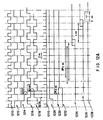
- Figures 12A and 12B are timing diagrams showing exemplary waveforms of the described system 400.
- System operation will be described with reference to the 480 MHz VCO output clock signal from phase-locked loop 440, which may be controllably time-shifted relative to the 240 MHz fixed pulse-repetition frequency of the UV output pulse train from laser subsystem 404. That is, the 480 MHz clock signal 1210 ( Figures 12A and 12B) supplied on output line 918 ( Figures 4 and 9) is varied in time relative to the output from reference oscillator 408 ( Figure 4), while the UV laser pulse train from laser subsystem 404 is fixed with respect to the output from reference oscillator 408 ( Figure 4).
- Waveform 1212 depicts the 480/2 MHz signal supplied at the output of divide-by-two circuit 914.
- Waveforms 1214, 1216 and 1218 respectively depict the 240 MHz repetition-rate UV laser pulses from laser subsystem 404 in sync, leading by 90°, and lagging by 90°, relative to waveform 1212. Again, it is to be noted that it is actually waveforms 1210 and 1212 which are shifted, while waveform 1214 remains fixed.
- Line 1220 of Figure 12A shows the timing of a train of laser/electron-beam pulses relative to the 480/2 MHz waveform 1212: when waveform 1212 is in sync with the laser/e-beam pulse train, the laser/e-beam pulse train is as shown by the dark lines (see arrow 1222); when waveform 1212 lags the laser/e-beam pulse train by 90°, the laser/e-beam pulse train is shifted as shown by arrow 1224; and when waveform 1212 leads the laser/e-beam pulse train by 90°, the laser/e-beam pulse train is shifted as shown by arrow 1226.
- fine-delay phase-locked loop 440 allows clock signal 1212 to be controllably phase-shifted in vernier fashion over a range of ⁇ 180° relative to the UV laser pulse train.
- the vernier-shift "window” is approximately 2 ns as shown at line 1220 in Figure 12A (1 / 480 MHz ⁇ 2.08 ns).
- An operating cycle of system 400 begins with an asynchronous enable (“start") signal ( Figure 12A, line 1228) supplied by data processing system 418 to AND gate 920 while restart line 1012 is high.
- the output of AND gate 920 is synchronized to clock signal 1212 by flip-flop 922, producing the sync enable signal ( Figure 12A, line 1230).
- the sync enable delayed signal ( Figure 12A, line 1232) on output line 942 of coarse delay counter 442 goes high at some integer number "n” of 480 MHz clock cycles after the sync enable signal ( Figure 12A, line 1230) goes high; the integer number is determined by the terminal count value loaded in coarse delay counter 442.
- Hold-off counter 924 is programmed to count any integer number "y" of 120 MHz clock cycles, so that its output waveform 1234 goes high at a programmable interval of approximately 8*y ns (more precisely, 1/120 MHz ⁇ 8.33 ) following the first rising edge of the 120 MHz clock signal after the sync enable delayed signal 1232 goes high.
- Beam unblank adjustable delay circuit 926 adds a further, programmable, vernier delay of "x" ns, as depicted by the waveform of line 1236.
- a beam unblank pulse of 3 ns width ( Figure 12A, line 1238) is produced by pulse picker 414 in response to signal 1236, to allow a single electron-beam pulse to pass through blanker 428 and into electron-beam column 426.
- Figure 12A illustrates how a single "sync enable" event (line 1230) and a single beam-unblank pulse (line 1238) are generated at programmably-controllable times relative to the 240 MHz laser/e-beam pulse train.
- Waveforms 1210, 1212, 1228, 1230 and 1232 of Figure 12A are repeated in Figure 12B for reference.
- Waveform 1232, sync enable delayed depicts the output signal from coarse timebase delay counter 442 (on output line 942 of Figure 9), which goes high approximately 2*n ns after sync enable waveform 1230 goes high; "n" is a terminal-count integer loaded into coarse delay counter 442 by data processing system 418.
- Waveform 1242 depicts the output of an exemplary one of the 20 output lines of register/mux 1024, which goes high approximately 2*m ns after waveform 1232 goes high (more precisely, m/480MHz ⁇ 2,08*m ns); "m" is a terminal-count integer loaded into counter/generator 1010 by data processing system 418.
- Waveform 1244 is the output of the corresponding one of the 20 vernier circuits 1028, with the rising edge delayed relative to that of waveform 1242 by a programmable interval of up to one 480 MHz clock cycle ( ⁇ 2.08 ns) as shown by arrow 1246. That is, the edge can go high at any time between time 1248 and 1250.
- Waveform 1252 shows the narrow pulse output from the corresponding one of the 20 edge-to-pulse generators 1032; if waveform 1244 went high at time 1248, then a narrow pulse 1254 is produced, and if waveform 1244 went high at time 1250, then a narrow pulse 1256 is produced.
- Waveform 1258 depicts the typical output signal from a "set” array of OR gates (e.g., OR gate array 1118 of Figure 11), comprising a series of pulses 1260, 1262, 1264, etc. It is noted that, due to the programmable nature of vernier circuits 1028, the pulses may be placed as desired relative to the 480 MHz VCO clock waveform 1210. Waveform 1266 depicts the typical output signal from a "reset” array of OR gates (e.g., OR gate array 1124 of Figure 11), comprising a series of pulses 1268, 1270, etc. Again, due to the programmable nature of vernier circuits 1028, the pulses may be placed as desired relative to the 480 VCO clock waveform 1210.
- Waveform 1272 depicts the typical output signal from S/R flip-flip 1120 on output line 1126 ( Figure 11), as derived from waveforms 1258 and 1266. That is, "set” pulse 1260 causes line 1126 to go high as indicated at 1274, "reset” pulse 1268 causes line 1126 to go low at time 1276, etc.
- laser subsystem 404 applies a UV output pulse train at a fixed pulse-repetition frequency of 240 MHz to photocathode assembly 430.
- the resultant electron beam sampling pulse train emitted by photocathode assembly 430 is then formed at 240 MHz, or is blanked by blanker 428 to form an integral submultiple of this frequency (e.g., 120 MHz, 80 MHz, 60 MHz, etc. ).
- Unblanking of blanker 428 is known as "pulse picking". Pulse picking is used where the time sweep of the sampled measurement exceeds one laser pulse repetition period.
- Figures 12A and 12B illustrate exemplary waveforms of one sampling measurement cycle, i.e., of one electron-beam probe pulse.
- Sampling measurements in accordance with the present invention are performed by varying the phase of the entire test program timing (e.g., shifting the phase of the test pattern applied to the DUT) relative to the fixed electron-beam sampling pulse train. This is in contrast to the prior-art technique of fixing the test pattern timing and varying the phase of the measurement sampling pulse.
- the 120 MHz signal output from reference oscillator 408 acts as a master clock to drive the "shutter" of the laser subsystem to produce the pulsed UV laser beam, and is also used to phase lock the 480 MHz voltage-controlled oscillator 910, which may be crystal-controlled if necessary for adequate stability.
- Phase discriminator 902 e.g., Analog Devices part number AD9901
- a programmable offset introduced by phase-locked loop 440 forces a phase shift of up to ⁇ 45° at 120 MHz (one cycle at 480MHz, or ⁇ 2.08ns) in the clock signal which drives coarse delay counter 442 and test pattern generator 416.
- Coarse-delay counter 442 is programmable to delay the start of the test pattern sequence by any desired number of 480 MHz clock cycles.
- the programmable, supplemental (fine) delay introduced by phase-locked loop 440 allows control to ⁇ 1 ps resolution.
- a GaAs D-type flip-flop 938 e.g., Gigabit Logic part number 10G021A
- a GaAs D-type flip-flop 938 e.g., Gigabit Logic part number 10G021A
- Non-linearity of 1% in the vernier phase shifter can cause up to 20 ps timebase error between vernier end points. This non-linearity can be characterized by, and a correction look up table created in, data processing system 418.
- a voltage-controlled phase shifter could be put in the 120 MHz signal path from reference oscillator to phase comparator 902.
- phase-lock scheme should provide sufficiently low jitter.
- jitter There is a trade off between jitter and the speed with which the phase changing can be done. Every ⁇ 2.08 ns along the time base, the phase of the 480 MHz oscillator has to change 360°. With a voltage controlled crystal oscillator this could take many ms. Also, even the phase changes for the timebase steps within the vernier range could take up to 1 ms to stabilize. Good jitter performance might be obtained with a non-crystal VCO but, if performance is to be improved, a crystal VCO may be used.
- GaAs devices are preferred for use as pin drivers 448. Simulations of GaAs driver circuits have shown that rise/fall times of 80 ps can be obtained, switching 20 mA into 50 ohms. However, packaging appears to be critical. It is preferred to use a GaAs integrated circuit or discrete components on an alumina substrate.
- the hybrid may be either leadless with all connections done by a Tektronix Hypcon elastomer connector to a printed circuit board or an SMA-type connector could contact the fast output directly on the hybrid.
- FIG. 13 is a simplified illustration of how the present invention may be employed in analyzing an electronic circuit.
- a test-vector pattern is applied by generator 416 to a target element 1302 of a wafer 504.
- the test vector pattern is synchronized to a timing reference 1303, as depicted in the "vector" window of display terminal 420.
- Electron beam pulses 1304 are applied to target element 1302, and secondary electrons 1306 are detected to supply a probe signal to data processing system 418.
- An event of probe signal (such as an edge 1308) may be related to a timing reference 1310, as shown in the "target" window of display terminal 420.
- the probe signal event may be aligned with the timing reference by adjusting the test vector pattern relative to timing reference 1303.
- Such adjustment may, for example, be made by displaying the signals as illustrated, and then giving commands to the data processing system 418 by keyboard or mouse pointer or the like.
- the electron-beam probe may be directed to element 1302 with the aid of "navigational” tools (employing CAD data, NET list data, schematic data, etc.) and the results displayed using "display” tools as described in U.S. Patent 4,706,019 and/or as embodied in the IDS 5000TM electron beam test probe system.
- an "electronic circuit” is intended to mean an integrated circuit, a hybrid circuit, an opto-electronic circuit, a multi-chip carrier module (MCM), or any other manufactured item having active and/or inactive elements and/or conductors which may be probed with an electron-beam test probe.
- MCM multi-chip carrier module
Landscapes
- Engineering & Computer Science (AREA)
- General Engineering & Computer Science (AREA)
- Physics & Mathematics (AREA)
- General Physics & Mathematics (AREA)
- Tests Of Electronic Circuits (AREA)
- Testing Or Measuring Of Semiconductors Or The Like (AREA)
Claims (21)
- Ein Elektronenstrahltestsondensystem für das Analysieren eines elektronischen Schaltkreises (504), welche Analyse die Messung des Potentials an ausgewählten Punkten des elektronischen Schaltkreises umfaßt, welches Elektronenstrahltestsondensystem umfaßt:a. eine Testsonde (402) miti. einer Photokatode (804) für das Erzeugen eines Zuges von Elektronenstrahlimpulsen (1220) in Reaktion auf einen Zug von Laserstrahlimpulsen;ii. Mittel (426, 428) für das Einwirkenlassen von Elektronenstrahlimpulsen, ausgewählt aus dem Zug von Elektronenstrahl impulsen auf einen elektronischen Schaltkreis, undiii. Mittel (528, 530) für das Messen des Potentials an einem Punkt innerhalb des elektronischen Schaltkreises durch Erfassen von Sekundärelektronen;b. ein Laseruntersystem (404) für das Erzeugen eines Zuges von Laserstrahlimpulsen mit einer stabilisierten Wiederholungsfrequenz (1214);c. einen optischen Koppler (452) für das Führen des Zuges von Laserstrahlimpulsen zu der Photokatode zur Erzeugung des Zuges von Elektronenstrahlimpulsen;d. einen Testmustergenerator (416), der auf einen Zeitbasisschaltkreis (412) reagiert für das Erzeugen eines formatierten Testmusters (1272), das synchronisiert ist auf die stabilisierte Wiederholungsfrequenz;e. Übertragungsleitungen (454) für das Zuführen des formatierten Testmusters zu dem zu analysierenden elektronischen Schaltkreis; undf. einen Zeitbasisschaltkreis (412), synchronisiert mit dem Laseruntersystem und angekoppelt an den Testmustergenerator (416) für das Einfügen einer programmierbaren Verzögerung zwischen einen Laserstrahlimpuls des Zuges von Laserstrahlimpulsen und das formatierte Testmuster,dadurch gekennzeichnet, daß die Länge des formatierten Testmusters und die Länge der programmierbaren Verzögerung größer sind als eine Periode der stabilisierten Wiederholungsfrequenz und daß der Zeitbasisschaltkreis (412) umfaßt:i. einen phasenverriegelten spannungsgesteuerten Oszillator (910), synchronisiert mit dem Laseruntersystem (404), welcher Oszillator dem Testmustergenerator ein Referenztaktsignal (1210) zuführt, dessen Phase abhängt von einer Referenzspannung, die dem Oszillator zugeführt wird;ii. Mittel (906, 904) für das Liefern einer programmierbaren Referenzspannung an den Oszillator zum Bewirken der Steuerung der Phase des Referenztaktsignals; undiii. einen programmierbaren Zähler (442) zum Zählen von Zyklen des Referenztaktsignals, zugeführt dem Testmustergenerator, welcher programmierbare Zähler ein Synchronisationssignal (1232) an den Testmustergenerator (416) liefert.
- Das Elektronenstrahltestsondensystem nach Anspruch 1, bei dem die Mittel (426) für das Anlegen von Elektronenstrahlimpulsen Mittel (616) umfassen für das Abtastenlassen der Elektronenstrahlimpulse über einen Bereich des elektronischen Schaltkreises, und bei dem das System ferner Mittel (418, 420) umfaßt, die auf die Potentialmeßmittel reagieren für das Erzeugen einer Abbildung von Potentialen auf Oberflächen innerhalb des elektronischen Schaltkreises.
- Das Elektronenstrahltestsondensystem nach Anspruch 1, bei dem der Zug von Elektronenstrahlimpulsen eine Impulswiederholungsrate aufweist gleich der stabilisierten Wiederholungsfrequenz, wobei die Testsonde einen steuerbaren Unterdrücker (428) für das Gattern der Elektronenstrahlimpulse umfaßt, und wobei das System ferner einen Pulsauswählschaltkreis (414) umfaßt für das Steuern des Unterdrückers zum Verringern der Elektronenstrahlimpulswiederholungsrate auf einen Bruchteil der stabilisierten Wiederholungsfrequenz.
- Das Elektronenstrahltestsondensystem nach Anspruch 1, bei dem das Laseruntersystem (404) umfaßt:i. einen modus-verriegelten IR-Infrarot-Laser (702);ii. einen ersten Frequenzverdoppler (728) zum Umsetzen von Licht von dem IR-Laser (702) in grünes Licht; undiii. einen zweiten Frequenzverdoppler (734) zum Umsetzen des grünen Lichts von dem ersten Frequenzverdoppler (728) in UV (ultra-violettes) Licht.
- Das Elektronenstrahltestsondensystem nach Anspruch 4, ferner umfassend einen elektronischen Phasenstabilisator (410), angekoppelt an das Laseruntersystem (404) für das Verringern von Phasenrauschen des Zuges von Laserstrahlimpulsen.
- Das Elektronenstrahltestsondensystem nach Anspruch 1, bei dem der optische Koppler eine optische Leitung (452) und eine Quarzlinse (802) für das Fokussieren der Laserstrahlimpulse auf die Photokatode (804) umfaßt.
- Das Elektronenstrahltestsondensystem nach Anspruch 6, bei dem der optische Koppler (452) eine optische Faser anstelle der optischen Leitung und eine Linse (742) für das Koppeln der Laserstrahlimpulse in die optische Faser umfaßt.
- Das Elektronenstrahltestsondensystem nach Anspruch 6, bei dem die optische Leitung (452) ein Lichtrohr umfaßt, das im wesentlichen freie Bewegung in mehreren Achsen zwischen dem Laseruntersystem (404) und der Photokatode ermöglicht, wobei das Lichtrohr ein gelenkiges Rohr mit mit Spiegeln versehenen Gelenken umfaßt.
- Das Elektronenstrahltestsondensystem nach Anspruch 1, bei dem die Photokatode (804) umfaßt:ein poliertes Quarzsubstrat;eine Schicht aus Calciumfluorid, aufgebracht auf einer Seite des polierten Quarzsubstrats; undeinen Goldfilm, der auf der Schicht aus Calciumfluorid aufgebracht ist.
- Das Elektronenstrahltestsondensystem nach Anspruch 9, bei dem die Mittel (426) für das Anlegen von Elektronenstrahlimpulsen eine evakuierte Elektronenstrahlsäule (426) umfassen mit einem Ende (812) mit einer öffnung für die Aufnahme der Photokatode (804), welche Photokatode in der öffnung aufgenommen ist, und mit Mitteln (816, 818, 820, 822, 824, 826, 828) für die hermetische Abdichtung der Stoßstelle zwischen der Photokatode (804) und dem Säulenende (812).
- Das Elektronenstrahltestsondensystem nach Anspruch 1, ferner umfassend Mittel (832, 834, 826) für das Halten der Photokatode (804) auf einem hohen negativen Potential relativ zur Masse.
- Das Elektronenstrahltestsondensystem nach Anspruch 11, bei dem die Mittel (426) für das Anlegen von Elektronenstrahlimpulsen eine Anode (806) umfassen, die auf hohem positivem Potential relativ zur Masse gehalten ist.
- Das Elektronenstrahltestsondensystem nach Anspruch 1, bei dem der Testmustergenerator (416) umfaßt:i. eine Schaltung (444), die auf ein Synchronisiersignal (1232) von dem Zeitbasisschaltkreis (412) reagiert für das Erzeugen eines Satzes von Zeitlageereignissignalen mit Zeitlageereignissen in gesteuerter zeitlicher Beziehung zu einem Startsignal (1228) und einem Referenztaktsignal (1210) und zueinander;ii. eine Logikmatrix (1114, 1118, 1124) für selektives Transformieren mindestens einiger der Zeitlageereignissignale in ein Muster von "Setz"- und "Rücksetz"signalen;iii. mindestens einen Schaltkreis (1120) für das Bilden des formatierten Testmusters aus dem Muster von "Setz-" und "Rücksetz"signalen; undiv. Mittel (1128) für das Ansteuern der elektronischen zu analysierenden Schaltung mit dem formatierten Testmuster.
- Das Elektronenstrahltestsondensystem nach Anspruch 13, bei dem die Schaltung (444) für das Erzeugen eines Satzes von Zeitlageereignissignalen mit Zeitlageereignissen in gesteuerter zeitlicher Beziehung zueinander programmierbare Vernier-Verzögerungselemente (1028) für die Steuerung der zeitlichen Beziehungen umfaßt.
- Das Elektronenstrahltestsondensystem nach Anspruch 1, bei dem die Übertragungsleitungen (454) mindestens eine Übertragungsleitung mit gesteuerter Impedanz und mindestens eine coplanare Übertragungsleitungssonde (424) mit hoher Bandbreite umfaßt.
- Das Elektronenstrahltestsondensystem nach Anspruch 1, bei dem die Mittel für das Messen des Potentials umfassen:i. Mittel (530, 528) für das Erfassen und Analysieren der Energie von Sekundärelektronen und für das Erzeugen eines entsprechenden Meßsignals; undii. ein Datenverarbeitungssystem (418, 420), angeschlossen zum Empfangen, Verarbeiten und graphisch Wiedergeben des Meßsignals.
- Das Elektronenstrahltestsondensystem nach Anspruch 16, bei dem die Mittel für das Messen des Potentials ferner Mittel (616) umfassen für das Richten der Elektronenstrahlimpulse auf einen ausgewählten Punkt innerhalb des elektronischen Schaltkreises unter Bezugnahme auf Konstruktionsdaten des elektronischen Schaltkreises.
- Das Elektronenstrahltestsondensystem nach Anspruch 9, bei dem das Quarzsubstrat beweglich ist, so daß der Zug von Laserstrahlimpulsen selektiv auf irgend einen Punkt einwirken kann innerhalb eines Bereichs der Photokatode, um so die Photokatode zu erneuern.
- Das Elektronenstrahltestsondensystem nach Anspruch 10, ferner umfassend Mittel (830) für das Positionieren des Quarzsubstrats derart, daß der Laserstrahlimpuls selektiv einwirken kann auf irgend einen Punkt innerhalb eines Bereichs der Photokatode, um so die Photokatode zu erneuern, und bei dem die Mittel (816-828) für das hermetische Abdichten ausgebildet sind, um eine solche Bewegung ohne Verlust an hermetischer Abdichtung zu ermöglichen.
- Das Elektronenstrahltestsondensystem nach Anspruch 4, bei dem der zweite Frequenzverdoppler (734) auf der Photokatodenbaugruppe (430) montiert ist und gekoppelt ist zum Empfang von grünem Laserlicht von dem ersten Frequenzverdoppler (728) über einen flexiblen optischen Koppler.
- Das Elektronenstrahltestsondensystem nach Anspruch 4, bei dem der erste Frequenzverdoppler (728) und der zweite Frequenzverdoppler (734) auf der Photokatodenbaugruppe (430) montiert sind, und der erste Frequenzverdoppler (728) angekoppelt ist zum Empfang von infrarotem Laserlicht von dem modusverriegelten IR-Laser über einen flexiblen optischen Koppler.
Applications Claiming Priority (2)
| Application Number | Priority Date | Filing Date | Title |
|---|---|---|---|
| US61992790A | 1990-11-28 | 1990-11-28 | |
| US619927 | 1990-11-28 |
Publications (2)
| Publication Number | Publication Date |
|---|---|
| EP0492677A1 EP0492677A1 (de) | 1992-07-01 |
| EP0492677B1 true EP0492677B1 (de) | 1996-06-12 |
Family
ID=24483887
Family Applications (1)
| Application Number | Title | Priority Date | Filing Date |
|---|---|---|---|
| EP91202756A Expired - Lifetime EP0492677B1 (de) | 1990-11-28 | 1991-10-24 | Photoemissionselektronenstrahlmesssonde mit gepulstem Laser |
Country Status (3)
| Country | Link |
|---|---|
| EP (1) | EP0492677B1 (de) |
| JP (1) | JPH05312925A (de) |
| DE (1) | DE69120233T2 (de) |
Families Citing this family (6)
| Publication number | Priority date | Publication date | Assignee | Title |
|---|---|---|---|---|
| EP0552048B1 (de) * | 1992-01-16 | 1999-04-21 | Hamamatsu Photonics K.K. | Anordnung zur Messung des zeitlichen Zusammenhangs zwischen zwei oder mehr Signalen |
| US5959458A (en) * | 1996-11-08 | 1999-09-28 | Schlumberger Technologies, Inc. | Method and apparatus for measuring electrical waveforms using atomic force microscopy |
| FR2844056B1 (fr) * | 2002-08-27 | 2005-04-29 | Centre Nat Etd Spatiales | Installation d'analyse d'un circuit integre |
| CN115410887B (zh) * | 2021-12-21 | 2026-04-07 | 中国科学院物理研究所 | 用于电子枪的激光引入装置及包括其的超快扫描电镜 |
| CN116449111B (zh) * | 2023-03-08 | 2025-07-18 | 重庆邮电大学 | 一种窄脉冲检测与计数电路 |
| KR20250140597A (ko) * | 2023-06-13 | 2025-09-25 | 주식회사 히타치하이테크 | 전자선 응용 장치 및 시간 상수 계측 방법 |
Family Cites Families (3)
| Publication number | Priority date | Publication date | Assignee | Title |
|---|---|---|---|---|
| US4963823A (en) * | 1988-06-27 | 1990-10-16 | Siemens Aktiengesellschaft | Electron beam measuring instrument |
| US5095262A (en) * | 1988-09-01 | 1992-03-10 | Photon Dynamics, Inc. | Electro-optic sampling system clock and stimulus pattern generator |
| DE3829770A1 (de) * | 1988-09-01 | 1990-04-19 | Brust Hans Detlef | Verfahren und anordnung zur asynchronen messung von signalverlaeufen |
-
1991
- 1991-10-24 EP EP91202756A patent/EP0492677B1/de not_active Expired - Lifetime
- 1991-10-24 DE DE1991620233 patent/DE69120233T2/de not_active Expired - Fee Related
- 1991-11-27 JP JP3312142A patent/JPH05312925A/ja active Pending
Non-Patent Citations (4)
| Title |
|---|
| - 410; M.BRUNNER ET AL.: 'Non-Invasive Waveform Measurements of IC-Internal GHz Signals in a ps Time Scale' * |
| EXTENDED ABSTRACTS, vol. 88-2, The Electrochemical Society, Fall Meeting 1988, pages 559-561 * |
| J. Vac. Sci. Technol. B6(6), November/December 1988, pages 2005-2008 * |
| MICROELECTRONIC ENGINEERING, vol. 12, nos. 1-4, May 1990, pages 213-220 * |
Also Published As
| Publication number | Publication date |
|---|---|
| EP0492677A1 (de) | 1992-07-01 |
| DE69120233D1 (de) | 1996-07-18 |
| JPH05312925A (ja) | 1993-11-26 |
| DE69120233T2 (de) | 1996-12-12 |
Similar Documents
| Publication | Publication Date | Title |
|---|---|---|
| US5270643A (en) | Pulsed laser photoemission electron-beam probe | |
| US7228464B2 (en) | PICA system timing measurement and calibration | |
| Fixl et al. | Laser stimulated electron-beam prober for 15 ps resolution internal waveform measurements of a 5 Gb/s ECL circuit | |
| Shinagawa et al. | An automated electro-optic probing system for ultra-high-speed IC's | |
| EP0492677B1 (de) | Photoemissionselektronenstrahlmesssonde mit gepulstem Laser | |
| Fujioka et al. | Function testing of bipolar ICs and LSIs with the stroboscopic scanning electron microscope | |
| May et al. | Picosecond photoelectron scanning electron microscope for noncontact testing of integrated circuits | |
| May et al. | Noncontact high-speed waveform measurements with the picosecond photoelectron scanning electron microscope | |
| US6154039A (en) | Functional OBIC analysis | |
| US20190227119A1 (en) | System and method of preparing integrated circuits for backside probing using charged particle beams | |
| Eiles et al. | Optical probing of VLSI ICs from the silicon backside | |
| Winkler et al. | Flexible picosecond probing of integrated circuits with chopped electron beams | |
| Lischke et al. | The limits of high-speed e-beam testing | |
| US5107124A (en) | Apparatus for modulating a particle beam intensity | |
| US4902963A (en) | Method and arrangement for recording periodic signals with a laser probe | |
| Gopinath et al. | High-resolution sampling SEM for quantitative investigations of semiconductor devices and integrated circuits | |
| Halbout et al. | Ultrashort electron-pulse probing of integrated circuits | |
| Keezer | Fault isolation and performance characterization of high speed digital multichip modules | |
| May et al. | Waveform measurements in high-speed silicon bipolar circuits using a picosecond photoelectron scanning electron microscope | |
| Brunner et al. | Non-invasive waveform measurements of IC-internal GHz signals in a ps time scale | |
| Weng et al. | Quantitative voltage measurement of high-frequency internal integrated circuit signals by scanning probe microscopy | |
| Thong et al. | Ultrahigh speed electron beam pulsing systems for electron beam testing | |
| May et al. | Picosecond photoelectron microscope for high-speed testing of integrated circuits | |
| Pastol et al. | Electron beam testing of integrated circuits using a picosecond photoelectron scanning electron microscope | |
| Chiu et al. | High‐speed electron beam testing |
Legal Events
| Date | Code | Title | Description |
|---|---|---|---|
| PUAI | Public reference made under article 153(3) epc to a published international application that has entered the european phase |
Free format text: ORIGINAL CODE: 0009012 |
|
| AK | Designated contracting states |
Kind code of ref document: A1 Designated state(s): DE FR GB IT NL |
|
| 17P | Request for examination filed |
Effective date: 19920925 |
|
| 17Q | First examination report despatched |
Effective date: 19940704 |
|
| GRAH | Despatch of communication of intention to grant a patent |
Free format text: ORIGINAL CODE: EPIDOS IGRA |
|
| GRAH | Despatch of communication of intention to grant a patent |
Free format text: ORIGINAL CODE: EPIDOS IGRA |
|
| GRAA | (expected) grant |
Free format text: ORIGINAL CODE: 0009210 |
|
| AK | Designated contracting states |
Kind code of ref document: B1 Designated state(s): DE FR GB IT NL |
|
| PG25 | Lapsed in a contracting state [announced via postgrant information from national office to epo] |
Ref country code: IT Free format text: LAPSE BECAUSE OF FAILURE TO SUBMIT A TRANSLATION OF THE DESCRIPTION OR TO PAY THE FEE WITHIN THE PRE;WARNING: LAPSES OF ITALIAN PATENTS WITH EFFECTIVE DATE BEFORE 2007 MAY HAVE OCCURRED AT ANY TIME BEFORE 2007. THE CORRECT EFFECTIVE DATE MAY BE DIFFERENT FROM THE ONE RECORDED.SCRIBED TIME-LIMIT Effective date: 19960612 Ref country code: NL Free format text: LAPSE BECAUSE OF FAILURE TO SUBMIT A TRANSLATION OF THE DESCRIPTION OR TO PAY THE FEE WITHIN THE PRESCRIBED TIME-LIMIT Effective date: 19960612 |
|
| ET | Fr: translation filed | ||
| REF | Corresponds to: |
Ref document number: 69120233 Country of ref document: DE Date of ref document: 19960718 |
|
| NLV1 | Nl: lapsed or annulled due to failure to fulfill the requirements of art. 29p and 29m of the patents act | ||
| PLBE | No opposition filed within time limit |
Free format text: ORIGINAL CODE: 0009261 |
|
| STAA | Information on the status of an ep patent application or granted ep patent |
Free format text: STATUS: NO OPPOSITION FILED WITHIN TIME LIMIT |
|
| 26N | No opposition filed | ||
| PGFP | Annual fee paid to national office [announced via postgrant information from national office to epo] |
Ref country code: GB Payment date: 19990928 Year of fee payment: 9 |
|
| PG25 | Lapsed in a contracting state [announced via postgrant information from national office to epo] |
Ref country code: GB Free format text: LAPSE BECAUSE OF NON-PAYMENT OF DUE FEES Effective date: 20001024 |
|
| GBPC | Gb: european patent ceased through non-payment of renewal fee |
Effective date: 20001024 |
|
| PGFP | Annual fee paid to national office [announced via postgrant information from national office to epo] |
Ref country code: FR Payment date: 20051006 Year of fee payment: 15 |
|
| PGFP | Annual fee paid to national office [announced via postgrant information from national office to epo] |
Ref country code: DE Payment date: 20051031 Year of fee payment: 15 |
|
| PG25 | Lapsed in a contracting state [announced via postgrant information from national office to epo] |
Ref country code: DE Free format text: LAPSE BECAUSE OF NON-PAYMENT OF DUE FEES Effective date: 20070501 |
|
| REG | Reference to a national code |
Ref country code: FR Ref legal event code: ST Effective date: 20070629 |
|
| PG25 | Lapsed in a contracting state [announced via postgrant information from national office to epo] |
Ref country code: FR Free format text: LAPSE BECAUSE OF NON-PAYMENT OF DUE FEES Effective date: 20061031 |