EP0493827A2 - Sensor für die Kontrolle des Fabrikationsprozesses einer Halbleitervorrichtung - Google Patents
Sensor für die Kontrolle des Fabrikationsprozesses einer Halbleitervorrichtung Download PDFInfo
- Publication number
- EP0493827A2 EP0493827A2 EP91122371A EP91122371A EP0493827A2 EP 0493827 A2 EP0493827 A2 EP 0493827A2 EP 91122371 A EP91122371 A EP 91122371A EP 91122371 A EP91122371 A EP 91122371A EP 0493827 A2 EP0493827 A2 EP 0493827A2
- Authority
- EP
- European Patent Office
- Prior art keywords
- semiconductor wafer
- scatter
- power
- coherent
- sensor
- Prior art date
- Legal status (The legal status is an assumption and is not a legal conclusion. Google has not performed a legal analysis and makes no representation as to the accuracy of the status listed.)
- Granted
Links
Images


Classifications
-
- H—ELECTRICITY
- H10—SEMICONDUCTOR DEVICES; ELECTRIC SOLID-STATE DEVICES NOT OTHERWISE PROVIDED FOR
- H10P—GENERIC PROCESSES OR APPARATUS FOR THE MANUFACTURE OR TREATMENT OF DEVICES COVERED BY CLASS H10
- H10P72/00—Handling or holding of wafers, substrates or devices during manufacture or treatment thereof
- H10P72/50—Handling or holding of wafers, substrates or devices during manufacture or treatment thereof for positioning, orientation or alignment
- H10P72/57—Mask-wafer alignment
-
- B—PERFORMING OPERATIONS; TRANSPORTING
- B24—GRINDING; POLISHING
- B24B—MACHINES, DEVICES, OR PROCESSES FOR GRINDING OR POLISHING; DRESSING OR CONDITIONING OF ABRADING SURFACES; FEEDING OF GRINDING, POLISHING, OR LAPPING AGENTS
- B24B37/00—Lapping machines or devices; Accessories
- B24B37/005—Control means for lapping machines or devices
- B24B37/013—Devices or means for detecting lapping completion
-
- G—PHYSICS
- G01—MEASURING; TESTING
- G01B—MEASURING LENGTH, THICKNESS OR SIMILAR LINEAR DIMENSIONS; MEASURING ANGLES; MEASURING AREAS; MEASURING IRREGULARITIES OF SURFACES OR CONTOURS
- G01B11/00—Measuring arrangements characterised by the use of optical techniques
- G01B11/02—Measuring arrangements characterised by the use of optical techniques for measuring length, width or thickness
- G01B11/06—Measuring arrangements characterised by the use of optical techniques for measuring length, width or thickness for measuring thickness ; e.g. of sheet material
- G01B11/0616—Measuring arrangements characterised by the use of optical techniques for measuring length, width or thickness for measuring thickness ; e.g. of sheet material of coating
-
- G—PHYSICS
- G01—MEASURING; TESTING
- G01B—MEASURING LENGTH, THICKNESS OR SIMILAR LINEAR DIMENSIONS; MEASURING ANGLES; MEASURING AREAS; MEASURING IRREGULARITIES OF SURFACES OR CONTOURS
- G01B11/00—Measuring arrangements characterised by the use of optical techniques
- G01B11/30—Measuring arrangements characterised by the use of optical techniques for measuring roughness or irregularity of surfaces
- G01B11/303—Measuring arrangements characterised by the use of optical techniques for measuring roughness or irregularity of surfaces using photoelectric detection means
-
- G—PHYSICS
- G03—PHOTOGRAPHY; CINEMATOGRAPHY; ANALOGOUS TECHNIQUES USING WAVES OTHER THAN OPTICAL WAVES; ELECTROGRAPHY; HOLOGRAPHY
- G03F—PHOTOMECHANICAL PRODUCTION OF TEXTURED OR PATTERNED SURFACES, e.g. FOR PRINTING, FOR PROCESSING OF SEMICONDUCTOR DEVICES; MATERIALS THEREFOR; ORIGINALS THEREFOR; APPARATUS SPECIALLY ADAPTED THEREFOR
- G03F7/00—Photomechanical, e.g. photolithographic, production of textured or patterned surfaces, e.g. printing surfaces; Materials therefor, e.g. comprising photoresists; Apparatus specially adapted therefor
- G03F7/70—Microphotolithographic exposure; Apparatus therefor
- G03F7/70483—Information management; Active and passive control; Testing; Wafer monitoring, e.g. pattern monitoring
-
- H—ELECTRICITY
- H10—SEMICONDUCTOR DEVICES; ELECTRIC SOLID-STATE DEVICES NOT OTHERWISE PROVIDED FOR
- H10P—GENERIC PROCESSES OR APPARATUS FOR THE MANUFACTURE OR TREATMENT OF DEVICES COVERED BY CLASS H10
- H10P72/00—Handling or holding of wafers, substrates or devices during manufacture or treatment thereof
- H10P72/04—Apparatus for manufacture or treatment
- H10P72/0451—Apparatus for manufacturing or treating in a plurality of work-stations
- H10P72/0468—Apparatus for manufacturing or treating in a plurality of work-stations comprising a chamber adapted to a particular process
-
- H—ELECTRICITY
- H10—SEMICONDUCTOR DEVICES; ELECTRIC SOLID-STATE DEVICES NOT OTHERWISE PROVIDED FOR
- H10P—GENERIC PROCESSES OR APPARATUS FOR THE MANUFACTURE OR TREATMENT OF DEVICES COVERED BY CLASS H10
- H10P72/00—Handling or holding of wafers, substrates or devices during manufacture or treatment thereof
- H10P72/06—Apparatus for monitoring, sorting, marking, testing or measuring
- H10P72/0604—Process monitoring, e.g. flow or thickness monitoring
-
- H—ELECTRICITY
- H10—SEMICONDUCTOR DEVICES; ELECTRIC SOLID-STATE DEVICES NOT OTHERWISE PROVIDED FOR
- H10P—GENERIC PROCESSES OR APPARATUS FOR THE MANUFACTURE OR TREATMENT OF DEVICES COVERED BY CLASS H10
- H10P72/00—Handling or holding of wafers, substrates or devices during manufacture or treatment thereof
- H10P72/06—Apparatus for monitoring, sorting, marking, testing or measuring
- H10P72/0612—Production flow monitoring, e.g. for increasing throughput
-
- H—ELECTRICITY
- H10—SEMICONDUCTOR DEVICES; ELECTRIC SOLID-STATE DEVICES NOT OTHERWISE PROVIDED FOR
- H10P—GENERIC PROCESSES OR APPARATUS FOR THE MANUFACTURE OR TREATMENT OF DEVICES COVERED BY CLASS H10
- H10P74/00—Testing or measuring during manufacture or treatment of wafers, substrates or devices
- H10P74/23—Testing or measuring during manufacture or treatment of wafers, substrates or devices characterised by multiple measurements, corrections, marking or sorting processes
- H10P74/238—Testing or measuring during manufacture or treatment of wafers, substrates or devices characterised by multiple measurements, corrections, marking or sorting processes comprising acting in response to an ongoing measurement without interruption of processing, e.g. endpoint detection or in-situ thickness measurement
-
- H—ELECTRICITY
- H10—SEMICONDUCTOR DEVICES; ELECTRIC SOLID-STATE DEVICES NOT OTHERWISE PROVIDED FOR
- H10P—GENERIC PROCESSES OR APPARATUS FOR THE MANUFACTURE OR TREATMENT OF DEVICES COVERED BY CLASS H10
- H10P74/00—Testing or measuring during manufacture or treatment of wafers, substrates or devices
- H10P74/20—Testing or measuring during manufacture or treatment of wafers, substrates or devices characterised by the properties tested or measured, e.g. structural or electrical properties
- H10P74/203—Structural properties, e.g. testing or measuring thicknesses, line widths, warpage, bond strengths or physical defects
Definitions
- a sensor system that includes a coherent electromagnetic or optical energy source that is configured to direct an incident energy beam perpendicular to and in the direction of semiconductor wafer surface.
- Components of the present invention measure those specular portions of the optical or electromagnetic energy that are coherently reflected by and coherently transmitted through the semiconductor wafer.
- the present invention also includes components for measuring the non-specular portions of electromagnetic or optical energy that are scattered in both reflectance from and transmittance through the semiconductor wafer.
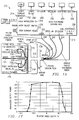
- the equipment parameters 42 are the easiest to monitor.
- the equipment parameters 42 can be directly adjusted and monitored by an operator, whereas the process 44 and wafer 46 parameters are usually dependent variables. Monitoring and control of the desired process 44 and wafer 46 parameters require specialized non-invasive in-situ sensors. Proper adjustments of process and wafer parameters are usually performed via varying the equipment parameters.
- the process parameters are functions of the equipment variables via equipment models and the wafer parameters are determined by the process parameters via process models.
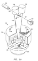
- An additional post-process in-situ sensor may be used for monitoring the gate dielectric thickness uniformity.
- the in-situ post-process uniformity sensor will assist in meeting the process uniformity specification and can provide delayed feedback process control information for process uniformity control, assuming the RTP module employs a multi-zone illuminator for dynamic and real-time uniformity control. If the temperature sensor monitors multiple points on wafer for dynamic uniformity control during the gate dielectric formation process, the post-process uniformity sensor will be non-critical.
- FIGURE 4 is a schematic diagram of a cluster tool setup 80 for CMOS metallization.
- the process sequence for metal (such as tungsten metallization) starts with a pre-clean for native oxide removal and continues with applying a layer via physical-vapor deposition (PVD) or sputtering and a CVD metal layer such as CVD tungsten.
- the critical real-time sensors for this cluster tool are temperature sensors and sheet resistant sensors to determine processed end-point. If necessary, one of the CVD metal chambers may be used for deposition of a barrier layer such as titanium nitride.
- a scattering ratio, S r can be defined as follows: S r ⁇ P sr (P sr + P cr )
- a transmitted scattering ratio can be determined as follows: S t ⁇ P st (P st + P ct )
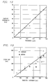
- KAMINS indicates that, at least to a first-order of magnitude, a linear relationship exists between tungsten film thickness and tungsten film average grain size.
- FIGURE 13 illustrates this relationship showing tungsten thickness ranging from 0 to 500 nm and grain size ranging from 0 to 450 nm.
- FIGURE 13 illustrates that with increasing CVD tungsten film thickness, average grain size increases almost linearly.
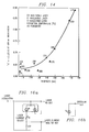
- FIGURE 19 illustrates the passage of semiconductor wafer 124 through the sensor heads 216 and 218 to establish the point at which RMS surface roughness measurements can be made using the method of the present invention.
- This sensor system can also perform multi-point measurements on a wafer. It is also possible to employ two diode laser sources with the sensor system of this invention in order to provide laser beam power simultaneously to the two sensor heads. The two laser sources may be modulated at two different frequencies.
Landscapes
- Physics & Mathematics (AREA)
- General Physics & Mathematics (AREA)
- Engineering & Computer Science (AREA)
- Mechanical Engineering (AREA)
- Testing Or Measuring Of Semiconductors Or The Like (AREA)
- Length Measuring Devices By Optical Means (AREA)
- Management, Administration, Business Operations System, And Electronic Commerce (AREA)
- Investigating Materials By The Use Of Optical Means Adapted For Particular Applications (AREA)
- Physical Vapour Deposition (AREA)
Applications Claiming Priority (4)
| Application Number | Priority Date | Filing Date | Title |
|---|---|---|---|
| US638468 | 1990-12-31 | ||
| US07/638,472 US5293216A (en) | 1990-12-31 | 1990-12-31 | Sensor for semiconductor device manufacturing process control |
| US638472 | 1990-12-31 | ||
| US07/638,468 US5270222A (en) | 1990-12-31 | 1990-12-31 | Method and apparatus for semiconductor device fabrication diagnosis and prognosis |
Publications (3)
| Publication Number | Publication Date |
|---|---|
| EP0493827A2 true EP0493827A2 (de) | 1992-07-08 |
| EP0493827A3 EP0493827A3 (en) | 1993-09-29 |
| EP0493827B1 EP0493827B1 (de) | 1996-02-28 |
Family
ID=27093091
Family Applications (1)
| Application Number | Title | Priority Date | Filing Date |
|---|---|---|---|
| EP91122371A Expired - Lifetime EP0493827B1 (de) | 1990-12-31 | 1991-12-30 | Sensor für die Kontrolle des Fabrikationsprozesses einer Halbleitervorrichtung |
Country Status (3)
| Country | Link |
|---|---|
| EP (1) | EP0493827B1 (de) |
| JP (1) | JPH06244261A (de) |
| DE (1) | DE69117480T2 (de) |
Cited By (10)
| Publication number | Priority date | Publication date | Assignee | Title |
|---|---|---|---|---|
| NL9401933A (nl) * | 1994-11-18 | 1996-07-01 | Tno | Documentensorteersysteem voor het sorteren van voor hercirculatie geschikte documenten, in het bijzonder bankbiljetten. |
| EP0647827A3 (de) * | 1993-10-12 | 1997-01-29 | Hughes Aircraft Co | Schichtdickenmessung auf einer diffus streuenden Oberfläche. |
| WO1999066548A1 (de) * | 1998-06-15 | 1999-12-23 | Steag Rtp Systems Gmbh | Verfahren zum bestimmen von parameterverteilungen von objekteigenschaften |
| EP0877308A3 (de) * | 1997-05-06 | 2000-08-23 | Tokyo Electron Limited | Steuerungsverfahren und -vorrichtung |
| DE19913922C2 (de) * | 1998-06-15 | 2002-10-24 | Steag Rtp Systems Gmbh | Verfahren zum Bestimmen von Parameterverteilungen von Substrateigenschaften |
| EP1271096A1 (de) * | 2001-06-18 | 2003-01-02 | Electronic Systems S.P.A. | Verfahren und Vorrichtung zur Messung der Dicke nichtmetallischer Schichten mit Hilfe einer Halbleiter-Infrarotstrahlungsquelle |
| EP1111657A3 (de) * | 1999-12-22 | 2005-09-07 | Applied Materials, Inc. | Steuerungssystem für mehrere Verarbeitungseinheiten |
| EP1124270A3 (de) * | 2000-02-11 | 2005-09-14 | Lucent Technologies Inc. | Herstellungsverfahren für piezoelektrische Filme mittels rotierendem Magnetronsputter-System |
| EP3495790A1 (de) * | 2017-12-05 | 2019-06-12 | Laser Systems & Solutions of Europe | Vorrichtung und verfahren zur messung der oberflächentemperatur eines substrats |
| EP4022108A4 (de) * | 2019-08-30 | 2024-02-14 | Applied Materials, Inc. | Elektronenstrahl-pvd-endpunkt-detektion und prozesssteuerungssysteme mit geschlossenem regelkreis |
Families Citing this family (7)
| Publication number | Priority date | Publication date | Assignee | Title |
|---|---|---|---|---|
| US6560503B1 (en) * | 1999-10-05 | 2003-05-06 | Advanced Micro Devices, Inc. | Method and apparatus for monitoring controller performance using statistical process control |
| US6985229B2 (en) * | 2002-05-30 | 2006-01-10 | Agere Systems, Inc. | Overlay metrology using scatterometry profiling |
| US20050275850A1 (en) * | 2004-05-28 | 2005-12-15 | Timbre Technologies, Inc. | Shape roughness measurement in optical metrology |
| JP4757456B2 (ja) * | 2004-07-01 | 2011-08-24 | 芝浦メカトロニクス株式会社 | 真空処理装置 |
| US8284394B2 (en) * | 2006-02-09 | 2012-10-09 | Kla-Tencor Technologies Corp. | Methods and systems for determining a characteristic of a wafer |
| DE102008049774B4 (de) * | 2008-09-30 | 2017-07-27 | Advanced Micro Devices, Inc. | Prozessanlage und Verfahren zur prozessinternen Überwachung der Metallkontamination während der Bearbeitung von Mikrostrukturen |
| DE102013006363A1 (de) | 2013-04-12 | 2014-10-30 | Guido Bell | Sensorik für die Unterscheidung von Dünnfilm-Solarmodulen |
Family Cites Families (2)
| Publication number | Priority date | Publication date | Assignee | Title |
|---|---|---|---|---|
| US4511800A (en) * | 1983-03-28 | 1985-04-16 | Rca Corporation | Optical reflectance method for determining the surface roughness of materials in semiconductor processing |
| US4707132A (en) * | 1985-08-05 | 1987-11-17 | Dutton G Wayne | Process for sensing defects on a smooth cylindrical interior surface in tubing |
-
1991
- 1991-12-27 JP JP34723391A patent/JPH06244261A/ja active Pending
- 1991-12-30 EP EP91122371A patent/EP0493827B1/de not_active Expired - Lifetime
- 1991-12-30 DE DE69117480T patent/DE69117480T2/de not_active Expired - Fee Related
Cited By (14)
| Publication number | Priority date | Publication date | Assignee | Title |
|---|---|---|---|---|
| EP0647827A3 (de) * | 1993-10-12 | 1997-01-29 | Hughes Aircraft Co | Schichtdickenmessung auf einer diffus streuenden Oberfläche. |
| NL9401933A (nl) * | 1994-11-18 | 1996-07-01 | Tno | Documentensorteersysteem voor het sorteren van voor hercirculatie geschikte documenten, in het bijzonder bankbiljetten. |
| EP0877308A3 (de) * | 1997-05-06 | 2000-08-23 | Tokyo Electron Limited | Steuerungsverfahren und -vorrichtung |
| US6258169B1 (en) | 1997-05-06 | 2001-07-10 | Tokyo Electron Limited | Control apparatus and control method |
| WO1999066548A1 (de) * | 1998-06-15 | 1999-12-23 | Steag Rtp Systems Gmbh | Verfahren zum bestimmen von parameterverteilungen von objekteigenschaften |
| DE19913922C2 (de) * | 1998-06-15 | 2002-10-24 | Steag Rtp Systems Gmbh | Verfahren zum Bestimmen von Parameterverteilungen von Substrateigenschaften |
| EP1111657A3 (de) * | 1999-12-22 | 2005-09-07 | Applied Materials, Inc. | Steuerungssystem für mehrere Verarbeitungseinheiten |
| EP1124270A3 (de) * | 2000-02-11 | 2005-09-14 | Lucent Technologies Inc. | Herstellungsverfahren für piezoelektrische Filme mittels rotierendem Magnetronsputter-System |
| EP1271096A1 (de) * | 2001-06-18 | 2003-01-02 | Electronic Systems S.P.A. | Verfahren und Vorrichtung zur Messung der Dicke nichtmetallischer Schichten mit Hilfe einer Halbleiter-Infrarotstrahlungsquelle |
| EP3495790A1 (de) * | 2017-12-05 | 2019-06-12 | Laser Systems & Solutions of Europe | Vorrichtung und verfahren zur messung der oberflächentemperatur eines substrats |
| WO2019110524A1 (en) * | 2017-12-05 | 2019-06-13 | Laser Systems & Solutions Of Europe | Apparatus and method for measuring the surface temperature of a substrate |
| TWI705234B (zh) * | 2017-12-05 | 2020-09-21 | 法商歐洲雷射系統與方案解決公司 | 用於測量基板的表面溫度之裝置及方法 |
| US11454543B2 (en) | 2017-12-05 | 2022-09-27 | Laser Systems & Solutions Of Europe | Apparatus and method for measuring the surface temperature of a substrate |
| EP4022108A4 (de) * | 2019-08-30 | 2024-02-14 | Applied Materials, Inc. | Elektronenstrahl-pvd-endpunkt-detektion und prozesssteuerungssysteme mit geschlossenem regelkreis |
Also Published As
| Publication number | Publication date |
|---|---|
| EP0493827A3 (en) | 1993-09-29 |
| JPH06244261A (ja) | 1994-09-02 |
| EP0493827B1 (de) | 1996-02-28 |
| DE69117480T2 (de) | 1996-06-13 |
| DE69117480D1 (de) | 1996-04-04 |
Similar Documents
| Publication | Publication Date | Title |
|---|---|---|
| US5293216A (en) | Sensor for semiconductor device manufacturing process control | |
| US5270222A (en) | Method and apparatus for semiconductor device fabrication diagnosis and prognosis | |
| EP0493827B1 (de) | Sensor für die Kontrolle des Fabrikationsprozesses einer Halbleitervorrichtung | |
| US5156461A (en) | Multi-point pyrometry with real-time surface emissivity compensation | |
| US5255286A (en) | Multi-point pyrometry with real-time surface emissivity compensation | |
| EP0655620B1 (de) | Auf Lichtstreuung basierende Temperaturmessung von Werkstücken in Echtzeit | |
| US5508934A (en) | Multi-point semiconductor wafer fabrication process temperature control system | |
| US5317656A (en) | Fiber optic network for multi-point emissivity-compensated semiconductor wafer pyrometry | |
| US8277281B2 (en) | Method and system for endpoint detection | |
| US5313044A (en) | Method and apparatus for real-time wafer temperature and thin film growth measurement and control in a lamp-heated rapid thermal processor | |
| US5118200A (en) | Method and apparatus for temperature measurements | |
| US5241366A (en) | Thin film thickness monitor | |
| US6958814B2 (en) | Apparatus and method for measuring a property of a layer in a multilayered structure | |
| KR100334706B1 (ko) | 반도체 공정에서 웨이퍼의 뒤틀림, 슬립변위, 및 그 분포를 측정하기 위한 시스템 | |
| WO2000012961A9 (en) | Combination thin-film stress and thickness measurement device | |
| EP1043759B1 (de) | Verfahren zur Verarbeitung von Siliziumwerkstücken mittels eines hybriden optischen Thermometerssystems | |
| US20060190211A1 (en) | In-situ wafer parameter measurement method employing a hot susceptor as radiation source for reflectance measurement | |
| Lehnert et al. | In situ spectroscopic ellipsometry for advanced process control in vertical furnaces | |
| Nguyenphu et al. | Wafer temperature measurement in a rapid thermal processor with modulated lamp power | |
| CN119290188A (zh) | 光栅测温装置、半导体设备及其测温方法 | |
| WO1996004534A1 (en) | Multipoint temperature monitoring apparatus for semiconductor wafers during processing | |
| JP2970020B2 (ja) | コーティング薄膜の形成方法 | |
| Bogdanowicz | Chromatic monitoring technique for thickness measurement of thin transparent films |
Legal Events
| Date | Code | Title | Description |
|---|---|---|---|
| PUAI | Public reference made under article 153(3) epc to a published international application that has entered the european phase |
Free format text: ORIGINAL CODE: 0009012 |
|
| AK | Designated contracting states |
Kind code of ref document: A2 Designated state(s): DE FR GB IT NL |
|
| PUAL | Search report despatched |
Free format text: ORIGINAL CODE: 0009013 |
|
| AK | Designated contracting states |
Kind code of ref document: A3 Designated state(s): DE FR GB IT NL |
|
| 17P | Request for examination filed |
Effective date: 19940324 |
|
| 17Q | First examination report despatched |
Effective date: 19940811 |
|
| GRAA | (expected) grant |
Free format text: ORIGINAL CODE: 0009210 |
|
| AK | Designated contracting states |
Kind code of ref document: B1 Designated state(s): DE FR GB IT NL |
|
| REF | Corresponds to: |
Ref document number: 69117480 Country of ref document: DE Date of ref document: 19960404 |
|
| ITF | It: translation for a ep patent filed | ||
| ET | Fr: translation filed | ||
| PLBE | No opposition filed within time limit |
Free format text: ORIGINAL CODE: 0009261 |
|
| STAA | Information on the status of an ep patent application or granted ep patent |
Free format text: STATUS: NO OPPOSITION FILED WITHIN TIME LIMIT |
|
| 26N | No opposition filed | ||
| REG | Reference to a national code |
Ref country code: GB Ref legal event code: IF02 |
|
| PGFP | Annual fee paid to national office [announced via postgrant information from national office to epo] |
Ref country code: FR Payment date: 20041201 Year of fee payment: 14 |
|
| PGFP | Annual fee paid to national office [announced via postgrant information from national office to epo] |
Ref country code: DE Payment date: 20041230 Year of fee payment: 14 |
|
| PG25 | Lapsed in a contracting state [announced via postgrant information from national office to epo] |
Ref country code: IT Free format text: LAPSE BECAUSE OF NON-PAYMENT OF DUE FEES;WARNING: LAPSES OF ITALIAN PATENTS WITH EFFECTIVE DATE BEFORE 2007 MAY HAVE OCCURRED AT ANY TIME BEFORE 2007. THE CORRECT EFFECTIVE DATE MAY BE DIFFERENT FROM THE ONE RECORDED. Effective date: 20051230 |
|
| PG25 | Lapsed in a contracting state [announced via postgrant information from national office to epo] |
Ref country code: DE Free format text: LAPSE BECAUSE OF NON-PAYMENT OF DUE FEES Effective date: 20060701 |
|
| PG25 | Lapsed in a contracting state [announced via postgrant information from national office to epo] |
Ref country code: FR Free format text: LAPSE BECAUSE OF NON-PAYMENT OF DUE FEES Effective date: 20060831 |
|
| PGFP | Annual fee paid to national office [announced via postgrant information from national office to epo] |
Ref country code: GB Payment date: 20061106 Year of fee payment: 16 |
|
| REG | Reference to a national code |
Ref country code: FR Ref legal event code: ST Effective date: 20060831 |
|
| PGFP | Annual fee paid to national office [announced via postgrant information from national office to epo] |
Ref country code: NL Payment date: 20071109 Year of fee payment: 17 |
|
| GBPC | Gb: european patent ceased through non-payment of renewal fee |
Effective date: 20071230 |
|
| PG25 | Lapsed in a contracting state [announced via postgrant information from national office to epo] |
Ref country code: GB Free format text: LAPSE BECAUSE OF NON-PAYMENT OF DUE FEES Effective date: 20071230 |
|
| NLV4 | Nl: lapsed or anulled due to non-payment of the annual fee |
Effective date: 20090701 |
|
| PG25 | Lapsed in a contracting state [announced via postgrant information from national office to epo] |
Ref country code: NL Free format text: LAPSE BECAUSE OF NON-PAYMENT OF DUE FEES Effective date: 20090701 |