EP0494536A2 - Operationschaltungsvorrichtung - Google Patents
Operationschaltungsvorrichtung Download PDFInfo
- Publication number
- EP0494536A2 EP0494536A2 EP91311974A EP91311974A EP0494536A2 EP 0494536 A2 EP0494536 A2 EP 0494536A2 EP 91311974 A EP91311974 A EP 91311974A EP 91311974 A EP91311974 A EP 91311974A EP 0494536 A2 EP0494536 A2 EP 0494536A2
- Authority
- EP
- European Patent Office
- Prior art keywords
- circuit device
- operational circuit
- bit data
- current
- analog
- Prior art date
- Legal status (The legal status is an assumption and is not a legal conclusion. Google has not performed a legal analysis and makes no representation as to the accuracy of the status listed.)
- Granted
Links
Images


Classifications
-
- G—PHYSICS
- G06—COMPUTING OR CALCULATING; COUNTING
- G06J—HYBRID COMPUTING ARRANGEMENTS
- G06J1/00—Hybrid computing arrangements
Definitions
- the present invention relates to an operational circuit device for calculation such as addition, multiplication and the like.
- a plurality of input digital signals are calculated by a digital operational circuit 71, and the calculated results are supplied to an analog converter 72 to obtain an analog signal.
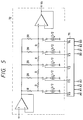
- Fig. 1 is a circuit diagram of an addition operational circuit device according to a first embodiment of the present invention.
- Reference numeral 1 represents an operational amplifier for outputting an analog reference voltage
- reference numerals 2 to 8 represent resistors connected in a ladder form constituting a resistor ladder unit 9.
- the values of the resistors 2, 3, 5, and 7 are R (ohm), and the values of the resistors 4, 6, and 8 are 2R (ohm).
- a voltage appears whose amplitude corresponds to the current states at interconnection points a , b , c , and d .
- Reference numeral 10 represents an operational amplifier for buffering an output voltage of the resistor ladder unit 9.
- Reference numerals 11 to 18 represent switches which are switched in accordance with inputted digital signals. If an input digital signal is "0", the switch is disconnected, and if "1", it is connected.
- the switches 11 and 12 are connected to the interconnection point a between the resistors 2 and 3, the switches 13 and 14 are connected to the interconnection point b between the resistors 3, 4, and 5, the switches 15 and 16 are connected to the interconnection point c between the resistors 5, 6, and 7, and the switches 17 and 18 are connected to the interconnection point d between the resistors 7 and 8.
- Reference numerals 19 to 26 represent constant current sources connected in series to corresponding switches 11 to 18.
- *A0 to *A3 and *B0 to *B3 are the inverted bits of input data A0 to A3 and B0 to B3.
- *A0 to *A3 are connected to the switches 11, 13, 15, and 17, and *B0 to *B3 are connected to the switches 12, 14, 16, and 18.
- Two input data A and B to be added together are inverted by inverters (not shown).
- the switch corresponding to the inverted bit *A0 to *A3 and *B0 to *B3 having a value "1" is connected to thereby flow a predetermined current from the corresponding constant current source.
- Such constant currents are summed up for each digit (0-th, 1st, 2nd, and 3rd) at the interconnection points a , b , c , and d and flow into the resistor ladder unit 9.
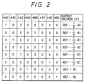
- FIG. 2 shows output voltages V0 when one of the bits *A0 to *A3 and *B0 to *B3 takes “1", and all the remaining bits take “0".
- addition can be carried out by adding currents for respective digits without using a digital adder, thereby reducing the circuit dimension.
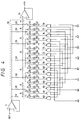
- Fig. 4 is a circuit diagram of a multiplication operational circuit device according to a second embodiment of the present invention.
- Reference numeral 1 represents an operational amplifier for outputting an analog reference voltage
- reference numeral 30 represents a resistor ladder unit for generating a voltage corresponding to the current states at interconnection points, similar to the first embodiment.
- Reference numeral 10 represents an operational amplifier for buffering an output voltage of the resistor ladder unit 30.
- Reference numerals 31 to 46 represent switches.
- Reference numerals 47 to 62 represent constant current sources connected in series to the corresponding switches 31 to 46.
- A0 to A3 and B0 to B3 are values at respective digits of input data A and B to be multiplied together.
- Reference numerals 63 to 78 represent NAND gates for performing a NAND operation for each term.
- the switches 31 to 46 are connected when an output of the corresponding NAND gates 63 to 78 takes "1".
- the NAND gates 63 to 78 carry out a multiplication operation for each term (A0 to A3, B0 to B3) of the input data A and B.
- the constant current sources 47 to 62, switches 31 to 46, interconnection points f to l carry out an addition of the multiplied results at the same term.
- the resistor ladder unit 30 carries out an addition operation for each digit including a carry.
- the switch corresponding to the bit *(A0 x B0) to * (A3 x B3) having a value "1" is connected to thereby flow a predetermined current from the corresponding constant current source.
- Such constant currents are summed up for each term at the interconnection points f to l and flow into the resistor ladder unit 30.
- V0 proportional to the sum of weighted currents at the interconnection points. Namely, the product for each term is carried out by the NAND gate, and the results are added together by the resistor ladder circuit to output the multiplication results.
- a digital multiplication circuit can be realized by one stage of NAND gates, resulting in a small circuit dimension and realizing high speed calculation.
Landscapes
- Engineering & Computer Science (AREA)
- Physics & Mathematics (AREA)
- Theoretical Computer Science (AREA)
- Computer Hardware Design (AREA)
- Mathematical Physics (AREA)
- Automation & Control Theory (AREA)
- Evolutionary Computation (AREA)
- Fuzzy Systems (AREA)
- General Physics & Mathematics (AREA)
- Software Systems (AREA)
- Analogue/Digital Conversion (AREA)
Applications Claiming Priority (2)
| Application Number | Priority Date | Filing Date | Title |
|---|---|---|---|
| JP3000557A JPH04251389A (ja) | 1991-01-08 | 1991-01-08 | 演算装置 |
| JP557/91 | 1991-01-08 |
Publications (3)
| Publication Number | Publication Date |
|---|---|
| EP0494536A2 true EP0494536A2 (de) | 1992-07-15 |
| EP0494536A3 EP0494536A3 (en) | 1993-02-03 |
| EP0494536B1 EP0494536B1 (de) | 1997-09-10 |
Family
ID=11477028
Family Applications (1)
| Application Number | Title | Priority Date | Filing Date |
|---|---|---|---|
| EP91311974A Expired - Lifetime EP0494536B1 (de) | 1991-01-08 | 1991-12-23 | Multiplikationsvorrichtung |
Country Status (4)
| Country | Link |
|---|---|
| US (1) | US5448506A (de) |
| EP (1) | EP0494536B1 (de) |
| JP (1) | JPH04251389A (de) |
| DE (1) | DE69127610T2 (de) |
Cited By (1)
| Publication number | Priority date | Publication date | Assignee | Title |
|---|---|---|---|---|
| WO2000017802A3 (en) * | 1998-09-21 | 2000-07-20 | Rn2R L L C | Adder and multiplier circuits employing logic gates having discrete, weighted inputs and methods of performing combinatorial operations therewith |
Families Citing this family (3)
| Publication number | Priority date | Publication date | Assignee | Title |
|---|---|---|---|---|
| US6188268B1 (en) * | 1998-10-30 | 2001-02-13 | Sony Corporation Of Japan | Low side current sink circuit having improved output impedance to reduce effects of leakage current |
| US6617989B2 (en) * | 2001-12-21 | 2003-09-09 | Texas Instruments Incorporated | Resistor string DAC with current source LSBs |
| US7002391B1 (en) * | 2003-03-27 | 2006-02-21 | Rf Micro Devices, Inc. | Selectable input attenuation |
Family Cites Families (14)
| Publication number | Priority date | Publication date | Assignee | Title |
|---|---|---|---|---|
| US3504360A (en) * | 1966-06-27 | 1970-03-31 | Sanders Associates Inc | Logic circuit producing an analog signal corresponding to an additive combination of digital signals |
| US3683165A (en) * | 1970-07-23 | 1972-08-08 | Computer Sciences Corp | Four quadrant multiplier using bi-polar digital analog converter |
| US3699568A (en) * | 1970-12-21 | 1972-10-17 | Motorola Inc | Weighted ladder technique |
| US3810157A (en) * | 1972-02-14 | 1974-05-07 | Sperry Rand Corp | Bipolar digital-to-analog converter |
| US3857021A (en) * | 1972-04-03 | 1974-12-24 | Hybrid Syst Corp | Multiplying current mode digital-to-analog converter |
| US4422155A (en) * | 1981-04-01 | 1983-12-20 | American Microsystems, Inc. | Multiplier/adder circuit |
| US4475170A (en) * | 1981-10-29 | 1984-10-02 | American Microsystems, Inc. | Programmable transversal filter |
| US4470126A (en) * | 1981-10-29 | 1984-09-04 | American Microsystems, Inc. | Programmable transversal filter |
| JPS61164338A (ja) * | 1985-01-17 | 1986-07-25 | Riken Denshi Kk | 多重演算型d/a変換器 |
| JPH0646709B2 (ja) * | 1985-02-28 | 1994-06-15 | キヤノン株式会社 | デジタル・アナログ変換器 |
| US4631522A (en) * | 1985-04-12 | 1986-12-23 | Audio Precision, Inc. | Method and circuit for compensation of a multiplying digital-to-analog converter |
| JPS61245718A (ja) * | 1985-04-24 | 1986-11-01 | Iwatsu Electric Co Ltd | デイジタル−アナログ変換器 |
| FR2620883A1 (fr) * | 1987-09-21 | 1989-03-24 | Thomson Semiconducteurs | Convertisseur numerique/analogique de sommes ponderees de mots binaires |
| US5311454A (en) * | 1993-02-08 | 1994-05-10 | Gulton Industries, Inc. | Digital multiplier-accumulator |
-
1991
- 1991-01-08 JP JP3000557A patent/JPH04251389A/ja active Pending
- 1991-12-23 DE DE69127610T patent/DE69127610T2/de not_active Expired - Fee Related
- 1991-12-23 EP EP91311974A patent/EP0494536B1/de not_active Expired - Lifetime
-
1994
- 1994-04-01 US US08/221,449 patent/US5448506A/en not_active Expired - Fee Related
Cited By (2)
| Publication number | Priority date | Publication date | Assignee | Title |
|---|---|---|---|---|
| WO2000017802A3 (en) * | 1998-09-21 | 2000-07-20 | Rn2R L L C | Adder and multiplier circuits employing logic gates having discrete, weighted inputs and methods of performing combinatorial operations therewith |
| US6205458B1 (en) | 1998-09-21 | 2001-03-20 | Rn2R, L.L.C. | Adder and multiplier circuits employing logic gates having discrete, weighted inputs and methods of performing combinatorial operations therewith |
Also Published As
| Publication number | Publication date |
|---|---|
| JPH04251389A (ja) | 1992-09-07 |
| DE69127610D1 (de) | 1997-10-16 |
| EP0494536A3 (en) | 1993-02-03 |
| DE69127610T2 (de) | 1998-01-22 |
| EP0494536B1 (de) | 1997-09-10 |
| US5448506A (en) | 1995-09-05 |
Similar Documents
| Publication | Publication Date | Title |
|---|---|---|
| US6003054A (en) | Programmable digital circuits | |
| EP0066251A2 (de) | Digital-Analog-Umwandler | |
| US4628276A (en) | Logarithmically linearly controlled variable gain amplifier | |
| EP0418184B1 (de) | Gegentaktdoppel-Digital-zu-Analog-Konverter | |
| KR940017236A (ko) | 아날로그 디지탈 컨버터 | |
| US3311910A (en) | Electronic quantizer | |
| EP0065795B1 (de) | DA-Wandler für bipolare Signale | |
| EP0494536A2 (de) | Operationschaltungsvorrichtung | |
| US3183342A (en) | Hybrid arithmetic unit | |
| JPH0783267B2 (ja) | 2進信号をこれに比例する直流信号に変換する装置 | |
| US3400257A (en) | Arithmetic operations using two or more digital-to-analog converters | |
| US5361219A (en) | Data circuit for multiplying digital data with analog | |
| EP0558243A2 (de) | Digital-/Analogumsetzer mit genauer linearer Ausgabe, sowohl für positive als auch für negative digitale Eingangsgrössen | |
| EP0373492A3 (de) | Wahrheitswerteflussverarbeitungseinheit | |
| US3810157A (en) | Bipolar digital-to-analog converter | |
| US3171022A (en) | Hybrid multiplier | |
| US5684483A (en) | Floating point digital to analog converter | |
| JPS5860821A (ja) | デジタル−アナログ変換出力装置 | |
| EP0177909A2 (de) | Digital-Analogwandler | |
| US4295123A (en) | Analog-to-digital converter | |
| ATE28015T1 (de) | Zustandsvariablenfilter. | |
| SU1640824A1 (ru) | Цифроаналоговый преобразователь | |
| SU935996A1 (ru) | Преобразователь перемещени в код | |
| SU739558A1 (ru) | Функциональный преобразователь с кусочно-линейной аппроксимацией | |
| JP2720156B2 (ja) | 信号発生装置 |
Legal Events
| Date | Code | Title | Description |
|---|---|---|---|
| PUAI | Public reference made under article 153(3) epc to a published international application that has entered the european phase |
Free format text: ORIGINAL CODE: 0009012 |
|
| AK | Designated contracting states |
Kind code of ref document: A2 Designated state(s): DE FR GB IT NL |
|
| PUAL | Search report despatched |
Free format text: ORIGINAL CODE: 0009013 |
|
| AK | Designated contracting states |
Kind code of ref document: A3 Designated state(s): DE FR GB IT NL |
|
| 17P | Request for examination filed |
Effective date: 19930618 |
|
| 17Q | First examination report despatched |
Effective date: 19950704 |
|
| GRAG | Despatch of communication of intention to grant |
Free format text: ORIGINAL CODE: EPIDOS AGRA |
|
| GRAH | Despatch of communication of intention to grant a patent |
Free format text: ORIGINAL CODE: EPIDOS IGRA |
|
| GRAH | Despatch of communication of intention to grant a patent |
Free format text: ORIGINAL CODE: EPIDOS IGRA |
|
| GRAA | (expected) grant |
Free format text: ORIGINAL CODE: 0009210 |
|
| AK | Designated contracting states |
Kind code of ref document: B1 Designated state(s): DE FR GB IT NL |
|
| PG25 | Lapsed in a contracting state [announced via postgrant information from national office to epo] |
Ref country code: IT Free format text: LAPSE BECAUSE OF FAILURE TO SUBMIT A TRANSLATION OF THE DESCRIPTION OR TO PAY THE FEE WITHIN THE PRE;WARNING: LAPSES OF ITALIAN PATENTS WITH EFFECTIVE DATE BEFORE 2007 MAY HAVE OCCURRED AT ANY TIME BEFORE 2007. THE CORRECT EFFECTIVE DATE MAY BE DIFFERENT FROM THE ONE RECORDED.SCRIBED TIME-LIMIT Effective date: 19970910 Ref country code: NL Free format text: LAPSE BECAUSE OF FAILURE TO SUBMIT A TRANSLATION OF THE DESCRIPTION OR TO PAY THE FEE WITHIN THE PRESCRIBED TIME-LIMIT Effective date: 19970910 |
|
| REF | Corresponds to: |
Ref document number: 69127610 Country of ref document: DE Date of ref document: 19971016 |
|
| ET | Fr: translation filed | ||
| NLV1 | Nl: lapsed or annulled due to failure to fulfill the requirements of art. 29p and 29m of the patents act | ||
| PLBE | No opposition filed within time limit |
Free format text: ORIGINAL CODE: 0009261 |
|
| STAA | Information on the status of an ep patent application or granted ep patent |
Free format text: STATUS: NO OPPOSITION FILED WITHIN TIME LIMIT |
|
| 26N | No opposition filed | ||
| REG | Reference to a national code |
Ref country code: GB Ref legal event code: IF02 |
|
| PGFP | Annual fee paid to national office [announced via postgrant information from national office to epo] |
Ref country code: DE Payment date: 20060224 Year of fee payment: 15 |
|
| PGFP | Annual fee paid to national office [announced via postgrant information from national office to epo] |
Ref country code: GB Payment date: 20061218 Year of fee payment: 16 |
|
| PG25 | Lapsed in a contracting state [announced via postgrant information from national office to epo] |
Ref country code: DE Free format text: LAPSE BECAUSE OF NON-PAYMENT OF DUE FEES Effective date: 20070703 |
|
| PGFP | Annual fee paid to national office [announced via postgrant information from national office to epo] |
Ref country code: FR Payment date: 20061218 Year of fee payment: 16 |
|
| GBPC | Gb: european patent ceased through non-payment of renewal fee |
Effective date: 20071223 |
|
| REG | Reference to a national code |
Ref country code: FR Ref legal event code: ST Effective date: 20081020 |
|
| PG25 | Lapsed in a contracting state [announced via postgrant information from national office to epo] |
Ref country code: GB Free format text: LAPSE BECAUSE OF NON-PAYMENT OF DUE FEES Effective date: 20071223 |
|
| PG25 | Lapsed in a contracting state [announced via postgrant information from national office to epo] |
Ref country code: FR Free format text: LAPSE BECAUSE OF NON-PAYMENT OF DUE FEES Effective date: 20071231 |