EP0494629B1 - Elektrische Stromversorgung - Google Patents
Elektrische Stromversorgung Download PDFInfo
- Publication number
- EP0494629B1 EP0494629B1 EP92100129A EP92100129A EP0494629B1 EP 0494629 B1 EP0494629 B1 EP 0494629B1 EP 92100129 A EP92100129 A EP 92100129A EP 92100129 A EP92100129 A EP 92100129A EP 0494629 B1 EP0494629 B1 EP 0494629B1
- Authority
- EP
- European Patent Office
- Prior art keywords
- voltage
- circuit
- current
- output
- load
- Prior art date
- Legal status (The legal status is an assumption and is not a legal conclusion. Google has not performed a legal analysis and makes no representation as to the accuracy of the status listed.)
- Expired - Lifetime
Links
- 238000001514 detection method Methods 0.000 claims description 44
- 238000004804 winding Methods 0.000 claims 1
- 238000010586 diagram Methods 0.000 description 34
- 239000003990 capacitor Substances 0.000 description 15
- 230000001276 controlling effect Effects 0.000 description 7
- 238000000926 separation method Methods 0.000 description 6
- 230000000694 effects Effects 0.000 description 5
- 230000005669 field effect Effects 0.000 description 3
- 230000001965 increasing effect Effects 0.000 description 3
- 230000015556 catabolic process Effects 0.000 description 2
- 230000008878 coupling Effects 0.000 description 2
- 238000010168 coupling process Methods 0.000 description 2
- 238000005859 coupling reaction Methods 0.000 description 2
- 230000006378 damage Effects 0.000 description 2
- 230000007423 decrease Effects 0.000 description 2
- 230000020169 heat generation Effects 0.000 description 2
- 230000004044 response Effects 0.000 description 2
- 239000000779 smoke Substances 0.000 description 2
- 230000004913 activation Effects 0.000 description 1
- 230000033228 biological regulation Effects 0.000 description 1
- 230000003028 elevating effect Effects 0.000 description 1
- 238000009499 grossing Methods 0.000 description 1
- 230000004048 modification Effects 0.000 description 1
- 238000012986 modification Methods 0.000 description 1
- 230000010355 oscillation Effects 0.000 description 1
- 230000001105 regulatory effect Effects 0.000 description 1
- 230000000391 smoking effect Effects 0.000 description 1
Images








Classifications
-
- H—ELECTRICITY
- H02—GENERATION; CONVERSION OR DISTRIBUTION OF ELECTRIC POWER
- H02M—APPARATUS FOR CONVERSION BETWEEN AC AND AC, BETWEEN AC AND DC, OR BETWEEN DC AND DC, AND FOR USE WITH MAINS OR SIMILAR POWER SUPPLY SYSTEMS; CONVERSION OF DC OR AC INPUT POWER INTO SURGE OUTPUT POWER; CONTROL OR REGULATION THEREOF
- H02M7/00—Conversion of AC power input into DC power output; Conversion of DC power input into AC power output
- H02M7/42—Conversion of DC power input into AC power output without possibility of reversal
- H02M7/44—Conversion of DC power input into AC power output without possibility of reversal by static converters
- H02M7/48—Conversion of DC power input into AC power output without possibility of reversal by static converters using discharge tubes with control electrode or semiconductor devices with control electrode
Definitions
- the present invention relates to a high-voltage AC power supply circuit adapted for use in an image forming apparatus such as a copying machine, printer or the like.
- US 4 962 307 describes an AC high-voltage power supply apparatus for use in an image forming apparatus including a load, comprising an AC high-voltage transformer to output AC high-voltage power and to supply an AC output to the load without rectifying the AC output and a load current detection circuit for detecting a DC component of a load current of the load.
- the known apparatus uses a constant voltage circuit instead of a constant current circuit and no diode element is connected to a DC constant current circuit in parallel, such that a current flowing in a direction of said diode element is opposite to that of said DC constant current circuit.
- a DC-DC converter circuit is inserted between a low voltage terminal and a ground terminal of a secondary coil of an AC high-voltage transformer, in order to control a DC current in an AC charging wire of a separating charger constituting a load.
- a DC-DC converter with a positive output and another DC-DC converter with a negative output are required.
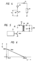
- Fig. 4 schematically shows the basic structure of the above-mentioned conventional example, wherein shown are an AC high-voltage power source 21 including an AC high-voltage transformer; a DC-DC converter 22; an output terminal P1; a separating charger 23 constituting a load; and a direct current i dc required for an electrostatic sheet separation.
- Said direct current i dc has to be in a direction opposite to the output of the DC-DC converter 22.
- Fig. 5 is a circuit diagram of said DC-DC converter 22, wherein the primary DC input to a transformer T31 is chopped by a switching transistor TR31 controlled by an output control circuit 31, and the generated secondary output is rectified and smoothed by a diode D31 and a capacitor C31.
- the secondary rectifying circuit is provided further with a breeder resistor R31.
- Fig. 6 shows the voltage-current characteristic of said DC-DC converter 22, indicating the DC voltage v dc and the direct current i dc respectively in the ordinate and in the abscissa.
- Fig. 7 shows the voltage-current characteristic of the separating charger 23 receiving power supply from said high-voltage AC power supply circuit, indicating the current i and voltage v respectively in the ordinate and in the abscissa. As shown in Fig. 7, the separating charger 23 has an apparently asymmetrical characteristic in the positive and negative sides, accepting more easily a current of the negative side.
- the resistance of the breeder resistor R31 has to be made infinitely small, in order to bring the direct current i dc to -400 ⁇ A.
- the DC-DC converter 22 has to be of a high power type, which gives rise to drawbacks of heat generation and high cost.
- control range of the direct current i dc is further spread from the limit of about zero in Fig. 6 to a positive area, it becomes necessary to serially insert a DC-DC converter 25 of a fixed output, with a polarity opposite to that of the variable-output DC-DC converter 22, as shown in Fig. 8. Since the control range of the direct current i dc in the load side becomes narrower by the output voltage of the fixed-output DC-DC converter 25, the output control range of the variable-output DC-DC converter 22 has to be accordingly widened, so that the power loss becomes even larger.
- the DC-DC converter 22 requires a small resistance in the freeder resistor R31 shown in Fig. 5, thus resulting in a significant power loss when the control range of the direct current i dc required for electrostatic sheet separation becomes wider. Also it requires a complex circuit structure.
- the object of the present invention is to provide an AC high-voltage power supply circuit, adapted for use in an image forming apparatus, and capable of controlling the DC component of the load current of a charger over a wide range from positive to negative side, with a simple structure and with a low power loss.
- Fig. 1 is a circuit diagram of an AC high-voltage power supply circuit, for electrostatic sheet separation in an electrophotographic copying machine, constituting a first embodiment of the present invention, wherein provided are an AC high-voltage transformer T1, and switching transistors TR1, TR2 for primary side drive, controlled by a control circuit 1 to provide a push-pull output. Output of a secondary high-voltage coil L2 of said transformer T1 is supplied, through an output terminal P1, to a separating charger constituting the load.
- an AC high-voltage transformer T1 and switching transistors TR1, TR2 for primary side drive, controlled by a control circuit 1 to provide a push-pull output.
- Output of a secondary high-voltage coil L2 of said transformer T1 is supplied, through an output terminal P1, to a separating charger constituting the load.
- a converter transformer T2 is provided for a constant voltage circuit, and a rectified positive output of the secondary side thereof is connected to the low voltage side of the secondary coil of the high-voltage transformer T1.
- the primary side of said converter transformer T2 is driven by a transistor TR11, and the output of said converter transformer T2 is controlled by regulation of the duty ratio of the collector current of said transistor TR11, through a pulse width modulation (PWM) circuit 11 connected to the base thereof.
- PWM pulse width modulation
- the secondary output of said transformer is rectified and smoothed by a diode D11 and a capacitor C11.
- a breeder resistor R11 is connected parallel to said capacitor C11, and a constant voltage circuit 2 is constituted by the above-explained structure.
- the low voltage side of the secondary coil of the converter transformer T2 of said constant voltage circuit is connected to the anode of a high-voltage diode D1 and the cathode of another high-voltage diode D2.
- the cathode of the high-voltage diode D1 is connected to the collector of a high-voltage transistor TR3, while the anode of the high-voltage diode D2 is connected to the emitter of the high-voltage transistor TR3.
- a diode varistor D61 is connected parallel to the high-voltage diode D2, for the purpose of circuit protection.
- a load current detection circuit 4 consisting of a resistor R1 and a capacitor C1, for detecting the DC component of the load current.
- Differential amplifiers OP1, OP2 compare the voltage detected by said detection circuit 4 with a reference voltage supplied to a terminal P2.
- the output of the differential amplifier OP1 is supplied to the base of the high-voltage transistor TR3, thereby controlling the base current thereof in such a manner that the detection output of the detection circuit 4 becomes equal to the reference voltage at the terminal P2.
- the high-voltage diode D1 and the high-voltage transistor TR3 constitute a DC constant current circuit 3 controlled by the detection output of the load current detection circuit 4.
- the output of the differential amplifier OP2 is supplied to the PWM circuit 11, thereby controlling the secondary rectified output of the converter transformer T2 in such a manner that the detection output of the detection circuit 4 becomes equal to the reference voltage at the terminal P2.
- the output of said constant voltage circuit 2 is controlled by the detection output of the load current detection circuit 4.
- the above-explained configuration enables to vary the DC component of the load current of the charger over a wider range from positive to negative side, with a higher efficiency and a reduced heat loss, and without the use of a power device or a heat sink.
- the circuit is protected from shortcircuiting of the load, resulting for example from the breakage of charging wires, and is therefore capable of preventing the accidents of fire or smoking resulting from spark leaking.
- the load current can be very easily controlled, since the serially connected DC constant current circuit and constant voltage circuit are not controlled independently but simultaneously by the voltage detected by the load current detection cricuit 4.
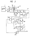
- Figs. 2 and 3 are circuit diagrams showing other embodiments, wherein parts same as or equivalent to those in the foregoing embodiment are represent by same symbols and will not be explained further.
- an integrating circuit 5 consisting of a resistor R12 and a capacitor C12, is inserted between the differential amplifier OP2 and the PWM circuit 11, in order to render the response speed of the constant voltage circuit 2, including the converter transformer T2, slower than that of the DC constant current circuit 3 including the high-voltage transistor TR3, thereby improving the stability of circuit operation.
- the difference in said response speeds can be arbitrarily selected by the resistor R12 and the capacitor C12.
- the constant voltage circuit involving the DC-DC converter shown in Fig. 1 is replaced by a tertiary coil L3 provided at the secondary side of the high-voltage transformer T1 and a shunt regulator 81 which constitutes a constant voltage circuit driven by the voltage generated in said tertiary coil L3 and is connected between the low voltage side of the high-voltage coil L2 of said high-voltage transformer T1 and the DC constant current circuit 3 consisting of the transistor TR3 and the diode D1.
- Said shunt regulator 81 is provided with a rectifying circuit consisting of a diode D23 and a capacitor C23.
- the output of the differential amplifier OP2 is supplied to the base of a transistor TR21 of the shunt regulator 81, and the collector current of said transistor TR21 is controlled by said output, or the voltage detected by the load current detection circuit 4, whereby the output voltage of the shunt regulator 81, across the capacitor C23 and the resistor R23, can be regulated.
- Said output is supplied, as in the foregoing embodiments, to the low voltage side of the high-voltage coil of the AC high-voltage transformer T1.
- the output of the differential amplifier OP1 is elevated to increase the collector current of the transistor TR3 in the DC constant current circuit 3, thereby increasing the load current in the negative direction.
- the output of the differential amplifier OP2 is also elevated to increase the collector current of the transistor TR21 of the shunt regulator 81.
- the output of the tertiary coil L3 of the high-voltage transformer T1 is lowered at the junction between the transistor TR21 and the capacitor C21, because of the voltage drop in the serial impedance of the resistor R21 and the capacitor C21, so that the output of the shunt regulator 81, corresponding to the double of said output voltage, is also lowered.
- the output of the shunt regulator 81 increases.
- the output of the differential amplifier OP1 is supplied, as in the foregoing embodiments, to the base of the high-voltage transistor TR3 of the DC constant current circuit 3, which is thus controlled by the detection output of the detection circuit 4.
- the 1st to 3rd embodiments explained above do not require a power device or a heat sink, since they are featured by a simple configuration with little power loss and without heat generation. Also since the serial connected DC constant current circuit and constant voltage circuit are not independently controlled but simultaneously by the output of the load current detection circuit, the load current can be very easily controlled and the DC component of the load current of the charger can be varied over a wide range, from positive to negative region.
- Fig. 9 is a circuit diagram of an AC high voltage generating device constituting a 4th embodiment of the present invention, wherein provided are an AC high-voltage transformer T1, switching transistors TR1, TR2 for primary side driving, and a push-pull output control circuit 1.
- the output of a high-voltage secondary coil of said high-voltage transformer T1 is supplied, through an output terminal P1, to an unrepresented separating charger constituting the load.
- the low voltage side P3 of the secondary coil of the high-voltage transformer T1 is connected to the anode of a high-voltage diode D1, the cathode of a high-voltage diode D2, and an end of a resistor R12.
- the cathode of the high-voltage diode D1 is connected to the collector of a high-voltage transistor Tr3, while the anode of the high-voltage diode D2 and the other end of the resistor R12 are connected to the emitter of said high-voltage transistor Tr3.
- Said components D1, TR3, R12 and D2 constitute a current control circuit 6.
- a detection circuit 3 consisting of a parallel circuit of a resistor R1 and a capacitor C1, for detecting the DC component of the load current.
- Said resistor R1 and capacitor C1 obtain the average of the load current.
- the voltage detected by said detection circuit 3 is compared with a reference voltage V R supplied to a terminal P2, in an error amplifier 2 in a control unit 7.
- the output of said error amplifier 2 serves to control the base current of the high-voltage transistor TR3 in such a manner that the detection output of the detection circuit 3 becomes equal to the reference voltage V R at the terminal P2.
- the power for the error amplifier 2 is supplied by a power source Ef in floating state. As a line of said power source is connected to the emitter of the high-voltage transistor TR3, the base current thereof does not flow into the current detection circuit 3.
- the value of the resistor R12 is determined in the following manner.
- Fig. 10 is an equivalent circuit diagram of the 4th embodiment shown in Fig. 9 and the charger constituting the load
- Fig. 11 is a voltage-current characteristic chart of the DC component (average of load current) of the current in the charger.
- Points A and B define the required control range of the DC component.
- the high-voltage transistor TR3 has to be turned on at the point A and off at the point B. Consequently, in the off-state of the high-voltage transistor TR3, the positive current has to be larger than the negative current by I 3 .
- V 1 /R LP - V 1 /(R LN + R12) I 3 wherein:
- R12 R LP 1 - (I 3 R LP )/V 1 - R LN
- the output of the detection circuit 3 is shifted in level by resistors R3, R4, into the input dynamic range of the error amplifier 2.
- resistors R3, R4 As the current in said resistors R, R4 also flows in the DC component detecting resistor R1, the resistances of R3, R4 have to be sufficiently large in order not to affect the accuracy of detection.
- the error amplifier 2 has to have a sufficiently large input impedance.
- an AC high voltage generating device of a high efficiency capable of controlling the DC current over a wide range covering positive and negative regions, without the use of a DC-DC converter. Since the error amplifier has a power source in floating state (hereinafter called floating power source), the DC component of the load current can be exactly detected.
- floating power source a power source in floating state
- Fig. 12 is a circuit diagram of a 5th embodiment, in which the differential amplifier 2 is powered by a common power source V cc , and a transistor TR4 of emitter follower connection is inserted between the output of said error amplifier 2 and the base of the high-voltage transistor TR3.
- An output line of a floating power source Ef is connected to the collector of the emitter follower transistor TR4, while the other output line of said power source Ef is connected to the emitter of the high-voltage transistor TR3.
- the present embodiment allows to simplify the floating power source, since it is only used for supplying the base current of the high-voltage transistor TR3.
- Fig. 13 is a circuit diagram of a 6th embodiment having a shortcircuiting protection circuit in the 4th embodiment.
- the output voltage of the AC high-voltage transformer T1 is applied between the collector and the emitter of the high-voltage transistor TR3.
- the embodiment shown in Fig. 9 may result in the destruction of the high-voltage transistor TR3, driving transistors TR1, TR2 for the AC high-voltage transformer T1, high-voltage diodes D1, D2 or resistor R12.
- an alternating current detection resistor R13 of which detection output is compared by a comparator with a predetermined value V R2 . If said detection output exceeds said predetermined value, the comparator sends a high-level output signal to the control circuit 1 for the AC high-voltage transformer T1, thereby terminating the activation of the switching transistors TR1, TR2.
- the 6th embodiment not only protects the circuit from shortcircuiting for example resulting from breakage of the charging wire but also can prevent fire or smoke generation by spark leaking. Also the alternating current detection for circuit protection from shortcircuiting is made possible without an additional rectifying circuit. Furthermore, said alternating current detection is made possible without affecting the precision of DC component detection in the load current.
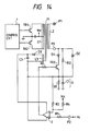
- Fig. 14 is a circuit diagram of a 7th embodiment in which the floating power supply Ef is obtained by rectifying and smoothing the output voltage of a tertiary coil L3 provided on the AC high-voltage transformer T1.
- Fig. 15 shows an 8th embodiment in which the floating power supply Ef is obtained by switching a transistor TR5 with the output of an oscillator circuit 5, and effecting double-voltage rectification on the switched output with capacitors C5, C6 and diodes D5, D6.
- Fig. 16 shows a 9th embodiment employing a high-voltage field effect transistor (FET) instead of the high-voltage bipolar transistor TR3.
- FET field effect transistor
- the 9th embodiment dispenses with the floating power source and allows to simplify the circuit structure, because of absence of current leak from the gate circuit of FET, based on the high input impedance thereof.
- the 4th to 9th embodiments explained above provide an AC high-voltage generating device of a high efficiency, capable of controlling the direct current over positive and negative regions, without the use of a DC-DC converter.
- the DC component of the load current can be exactly detected by the use of a floating power source.
- the floating power source may be dispensed with by the use of a field effect transistor in the current control circuit.
- Fig. 7 is a circuit diagram of an AC high-voltage generating circuit, adapted for electrostatic sheet separation in an electro-photographic copying apparatus, constituting a 10th embodiment of the present invention, wherein provided are an AC high-voltage transformer T1, and switching transistors TR1, TR2 for primary driving, driven by a control circuit 1 to generate a push-pull output.
- the output of a secondary high-voltage coil L2 of said AC high-voltage transformer T1 is supplied, through an output terminal P1, to a separating charger constituting the load.
- the other end of the secondary high-voltage coil of the high-voltage transformer T1 is connected to a current control circuit consisting of serial connection of a high-voltage diode D1 and a serial regulator 4, and also to a parallel circuit consisting of a high-voltage diode D2 and a resistor R12.
- Said serial regulator 4 is composed of serial connection of high-voltage transistors TR3, TR4 and serves to control the negative component of a separating corona current, which is the load current, by a variation in the base current of said transistor TR3 as will be explained later.
- a diode D2 is provided for bypassing the positive component in the opposite direction.
- the resistor R12 determines the amount of negative component in the load current when the serial regulator 4 is cut off.
- a detection circuit 3 for detecting the DC component of the load current consisting of parallel connection of a resistor R1 and a capacitor C1.
- the voltage detected by said detection circuit 3 is compared with a reference voltage CR supplied to a terminal P2, by a differential amplifier 2, of which output controls the base current of the transistor TR3 in such a manner that the output of the detection circuit 3 becomes equal to said reference voltage VR.
- Said differential amplifier 2 is powered by a floating power source EF1. Since the other end of said floating power source EF1 is connected to the emitter of the transistor TR3, the base current thereof does not flow into the current detecting resistor R1.
- the value of the resistor R12 is determined in the following manner.
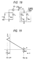
- Fig. 18 is a schematic equivalent circuit diagram of the power supply circuit of the 10th embodiment shown in Fig. 17 and the load charger, and Fig. 19 is a voltage-current characteristic chart of the DC component of the charger.
- points A and B define the required control range of the DC component.
- the transistor TR3 has to be turned on at the point A and off at the point B, and, in the turned-off state of the transistor TR3, the positive current has to be larger than the negative current by I 3 .
- V 1 /R LP - V 1 /(R LN + R 12 ) I 3 wherein:
- the detection output of the DC component detection circuit 3 has to be shifted in level by resistors R3, R4 so as to fit into the input dynamic range of the differential amplifier 2.
- the values of said resistors R3, R4 have to be sufficiently large, in order not to affect the precision of detection, since the current in said resistors R3, R4 also flows in the DC component detecting resistor R1.
- the differential amplifier 2 constituting control means for controlling the base current of the transistor TR3 of the serial regulator 4 according to the output of the detection circuit 3 for the DC component of the load current, is to have a sufficiently large input impedance, for a similar reason to that for the resistors R3, R4.
- the above-explained configuration divides the secondary high-voltage current of the AC high-voltage transformer T1 into positive and negative DC currents by the diodes D1 and D2, and controls the DC component of the load current by the serial regulator 4 constituting the current control circuit, inserted in one of thus divided currents.
- the resistor R12 inserted parallel to the current control circuit, has a resistance larger than the difference between the positive and negative pseudo equivalent resistances of the load charger.
- the output voltage of the serial regulator 4 in the current control circuit has to be variable over a wide range. Since the serial regulator 4 divides the applied voltage by serial connection of plural transistors TR3, TR4, it is not restricted by the breakdown voltage of respective transistor. Thus the DC component of the load current of the charger can be controlled over a wide range including positive and negative regions, by the control of base current of the transistor in said serial regulator 4 according to the result of comparison of the output of the detection circuit 3 with the reference voltage VR in the operational amplifier 2.
- the configuration of the present embodiment is featured by a simpler structure and a lower power loss, in comparison with the conventional devices.
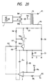
- Fig. 20 is a circuit diagram of an 11th embodiment of the present invention, wherein parts same as or equivalent to those in the 10th embodiment are represented by same symbols and will not be explained further.
- the resistors R6, R7 provided parallel to the serial regulator 4 are so selected that they have a summed resistance equal to the resistance of the resistor R12 in the 10th embodiment, thereby dispensing with said resistor R12.
- the resistance of a resistor R8 provided between the base and the emitter of the transistor TR3 is selected sufficiently smaller than that of the resistors R6, R7 and can therefore be considered negligible.
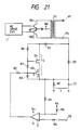
- Fig. 21 is a circuit diagram of a 12th embodiment of the present invention, wherein parts same as or equivalent to those in the 10th embodiment are represented by same symbols and will not be explained further.
- high-voltage field effect transistors (FET) Q3, Q4 are employed for the high-voltage transistors TR3, TR4 in the serial regulator 4.
- the output of the differential amplifier 2 controls the gate voltage of the FET Q3. Since there is no current leak from the gate G to the source S or drain D, the power source for the differential amplifier 2 need not be in the floating state. Consequently the circuit structure is simplified, and still a same effect as in the 10th embodiment can be attained.
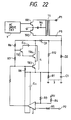
- Fig. 22 is a circuit diagram of a 13th embodiment of the present invention, wherein parts same as or equivalent to those in the 12th embodiment are represented by same symbols and will not be explained further.
- the potential at the junction of the resistors R6 and R7 is given to the base of the transistor TR4 through a transistor TR5 of emitter follower connection.
- the collector of said transistor TR5 is connected to a floating power source EF2, having the reference at the emitter of the transistor TR4.
- Base resistors R6, R7 of the transistors TR3, TR4 have resistances in a range from several hundred ohms to several kilo-ohms for elevating the destruction voltages of said transistors.
- Fig. 23 illustrates an example of the floating power sources EF1, EF2 for the 13th embodiment.
- a high frequency oscillator circuit 5 drives a pulse transformer T, of which secondary output is rectified to provide a floating power source EF1 for the differential amplifier 2 and a floating power source for the emitter follower transistor TR5.
- the above-explained configuration provides an effect similar to that in the 10th embodiment, without the limitation in the variable range of the load current resulting from the base current of the high-voltage transistors TR3, TR4 constituting the serial regulator 4.
- Fig. 24 is a circuit diagram of a 14th embodiment, wherein parts same as or equivalent to those in the foregoing embodiment are represented by same symbols and will not be explained further.
- the floating power supplies EF1, EF2 are obtained, not from a pulse transformer but from a capacity-coupled rectifying circuit.
- the output frequency of the oscillator circuit 5 is selected as high as possible, in order to minimize the coupling capacity between the rectifying circuit and the oscillator circuit.
- the oscillation frequency is selected as 500 KHz
- coupling capacitors C42, C43, C44 and C45 are selected as 100 pF.
- the above-explained configuration provides an effect similar to that in the 13th embodiment, while reducing the cost of the floating power source and minimizing the attenuation of the AC high-voltage output.
- the circuits of the 10th to 14th embodiments can control the DC component of the load current, by dividing the secondary high-voltage current of the AC high-voltage transformer into positive and negative DC currents by diodes, and inserting a current control circuit in one of thus divided currents.
- the DC component of the load current can be controlled over a wide range including positive and negative regions, since the resistor positioned parallel to the current control circuit has a resistance larger than the difference between the positive and negative pseudo equivalent resistances of the load charger.
- the serial regulator is composed of serial connection of plural transistors, it is not limited by the breakdown voltage of respective transistor, and the DC component of the load current of the charger constituting the load can be controlled over a wide range, from positive to negative region, through the control of base current of the transistor constituting said serial regulator, according to the output of the detection circuit. Also the circuits of said embodiments are featured by a simpler structure and a lower power loss, in comparison with conventional circuits.
- the present invention enables to vary the DC component of an AC output in a simple manner over a wide range including positive and negative regions.
- an AC high-voltage power supply circuit adapted for use in an image forming apparatus, for example in the separation charger of an electrophotographic copier, and capable of controlling the DC component in an AC high voltage, over a wide range including positive and negative regions.
- the power supply circuit comprises, at the low voltage side of a secondary coil of an AC high-voltage transformer, a DC constant current circuit consisting of a transistor and a diode, a constant voltage circuit connected oppositely in polarity to the DC constant current circuit, and a detection circuit for detecting the DC component of a load current, and the outputs of the constant voltage circuit and of the DC constant current circuit are controlled according to the output of the detection circuit.
- the device is featured by a simpler structure, a wider control range of the DC component including positive and negative regions, and a lower power loss.
Landscapes
- Engineering & Computer Science (AREA)
- Power Engineering (AREA)
- Dc-Dc Converters (AREA)
- Electrostatic Charge, Transfer And Separation In Electrography (AREA)
Claims (5)
- Wechselhochspannungs- Stromversorgungsgerät zur Versorgung einer Last in einem Bilderzeugungsgerät, miteinem Wechselhochspannungstransformator (T1) mit wenigstens einer Sekundärwicklung, deren erster Anschluß (P1) mit der Last verbunden ist, und deren zweiter Anschluß mit einer Konstantgleichstromschaltung (3) verbunden ist, die einen Transistor (TR3) enthält, der in Serie mit einer Laststrom-Feststellschaltung (4) zur Feststellung einer Gleichstromkomponente des Laststroms der Last geschaltet ist, und miteinem Diodenelement (D2), das mit der Konstantgleichstromschaltung (3) parallel geschaltet ist, so daß ein Strom in einer Richtung des Diodenelements (D2) fließt, die derjenigen der Konstantgleichstromschaltung (3) entgegengesetzten ist, und miteiner Rückkoppelsteuerschaltung (OP1, OP2, P2) zur Steuerung der Konstantgleichstromsteuerschaltung (3) auf der Grundlage eines Ausgangssignals der Laststrom- Steuerschaltung (4).
- Gerät nach Anspruch 1, das des weiteren ausgestattet ist mit einer Konstantspannungsschaltung (2), die in Serie mit der Konstantgleichstromschaltung (3) und dem Transformator (T1) geschaltet ist.
- Gerät nach Anspruch 2, dessen Rückkopplungssteuerschaltung (OP1, OP2, P2) die Konstantgleichspannungsschaltung (2) auf der Grundlage des Ausgangssignals der Laststrom- Feststellschaltung (4) steuert.
- Gerät nach Anspruch 1, das des weiteren mit einem Diodenvaristor (61) ausgestattet ist, der parallel zur Konstantstromschaltung (3) und zum Diodenelement (D2) geschaltet ist.
- Gerät nach Anspruch 1, dessen Konstantgleichstromschaltung (3) eine zweite Diode (D1) enthält, deren Richtung dem Diodenelement (D2) entgegengesetzt ist.
Applications Claiming Priority (6)
| Application Number | Priority Date | Filing Date | Title |
|---|---|---|---|
| JP620/91 | 1991-01-08 | ||
| JP03000620A JP3105549B2 (ja) | 1991-01-08 | 1991-01-08 | 画像形成装置の高圧交流電源回路 |
| JP04164291A JP3210026B2 (ja) | 1991-03-07 | 1991-03-07 | Ac高圧発生装置 |
| JP41642/91 | 1991-03-07 | ||
| JP23125191A JP3195620B2 (ja) | 1991-09-11 | 1991-09-11 | 画像形成装置の高圧交流電源回路 |
| JP231251/91 | 1991-09-11 |
Publications (3)
| Publication Number | Publication Date |
|---|---|
| EP0494629A2 EP0494629A2 (de) | 1992-07-15 |
| EP0494629A3 EP0494629A3 (en) | 1992-10-21 |
| EP0494629B1 true EP0494629B1 (de) | 1997-08-20 |
Family
ID=27274535
Family Applications (1)
| Application Number | Title | Priority Date | Filing Date |
|---|---|---|---|
| EP92100129A Expired - Lifetime EP0494629B1 (de) | 1991-01-08 | 1992-01-07 | Elektrische Stromversorgung |
Country Status (3)
| Country | Link |
|---|---|
| US (1) | US5532913A (de) |
| EP (1) | EP0494629B1 (de) |
| DE (1) | DE69221644T2 (de) |
Families Citing this family (13)
| Publication number | Priority date | Publication date | Assignee | Title |
|---|---|---|---|---|
| ES2100803B1 (es) * | 1994-05-20 | 1998-04-16 | Telefonica Nacional Espana Co | Circuito integrado de actuacion y exploracion doble. |
| JP3647166B2 (ja) * | 1996-09-11 | 2005-05-11 | キヤノン株式会社 | 電源回路 |
| US5815381A (en) * | 1997-06-06 | 1998-09-29 | Burr-Brown Corporation | Single-barrier closed loop DC-to-DC converter and method |
| JP4314709B2 (ja) * | 1999-12-28 | 2009-08-19 | ソニー株式会社 | スイッチング電源装置 |
| JP4556331B2 (ja) * | 2001-01-22 | 2010-10-06 | 株式会社豊田自動織機 | スイッチング電源回路 |
| CA2417395A1 (en) * | 2002-01-28 | 2003-07-28 | James William Haslett | Monolithic transformer compensated circuit |
| DE102004010169B4 (de) * | 2004-03-02 | 2010-09-02 | Infineon Technologies Ag | Schaltungsanordnung und Verfahren zur Reduzierung von Übersprechen sowie Verwendung derartiger Schaltungsanordnungen |
| US20060006849A1 (en) * | 2004-06-28 | 2006-01-12 | Haslett James W | Inductor compensating circuit |
| KR102086596B1 (ko) * | 2013-07-03 | 2020-04-14 | 휴렛-팩커드 디벨롭먼트 컴퍼니, 엘.피. | 화상형성장치 및 화상형성장치의 전원 공급 방법 |
| US9337714B2 (en) * | 2014-02-06 | 2016-05-10 | Dialog Semiconductor Inc. | Power converter with fast discharge circuit |
| US9904232B2 (en) | 2015-02-18 | 2018-02-27 | Canon Kabushiki Kaisha | Power supply apparatus and image forming apparatus |
| CN108964468B (zh) * | 2016-05-03 | 2020-07-17 | 苏州泰思特电子科技有限公司 | 用于多种电压等级的高压发生器 |
| JP7066538B2 (ja) * | 2018-06-07 | 2022-05-13 | キヤノン株式会社 | 電源装置及び画像形成装置 |
Family Cites Families (18)
| Publication number | Priority date | Publication date | Assignee | Title |
|---|---|---|---|---|
| GB1551013A (en) * | 1975-11-07 | 1979-08-22 | Rca Corp | Power supply arrangement with minimum interaction between plural loads |
| JPS54139736A (en) * | 1978-04-21 | 1979-10-30 | Sharp Corp | Electrophotographic copier |
| JPS5936151Y2 (ja) * | 1979-09-18 | 1984-10-05 | シャープ株式会社 | 電源回路 |
| US4868729A (en) * | 1982-02-16 | 1989-09-19 | Canon Kabushiki Kaisha | Power supply unit |
| JPH078139B2 (ja) * | 1983-09-02 | 1995-01-30 | キヤノン株式会社 | 高圧電源 |
| US4791544A (en) * | 1984-09-21 | 1988-12-13 | Veeco Instruments | Regulating control for single-ended switching power supply |
| US4727463A (en) * | 1985-06-13 | 1988-02-23 | Canon Kabushiki Kaisha | Power supply device comprising means for modulating the output thereof |
| US4791528A (en) * | 1985-06-13 | 1988-12-13 | Canon Kabushiki Kaisha | Power supply device |
| EP0261894B1 (de) * | 1986-09-20 | 1996-04-10 | Canon Kabushiki Kaisha | Leistungsquellenapparat |
| NL8701846A (nl) * | 1987-08-05 | 1989-03-01 | Merrillton Corp N V | Elektrisch voedingsapparaat met een gereguleerde wisselspanningsuitgang. |
| US4968106A (en) * | 1987-12-04 | 1990-11-06 | Murata Manufacturing Co., Ltd. | High voltage generating apparatus for television equipment |
| JP2773195B2 (ja) * | 1988-04-05 | 1998-07-09 | 松下電器産業株式会社 | スイッチング電源装置 |
| US4962307A (en) * | 1988-04-21 | 1990-10-09 | Ricoh Company, Ltd. | Corona discharging device |
| EP0343392B1 (de) * | 1988-05-09 | 1992-09-23 | Siemens Aktiengesellschaft | Anordnung zum Nachbilden einer Wechselgrösse bei einem gesteuerten Halbleiter |
| US5173847A (en) * | 1988-09-30 | 1992-12-22 | Canon Kabushiki Kaisha | PWM power supply with synchronous rectifier and synchronizing oscillator |
| US4866587A (en) * | 1988-12-22 | 1989-09-12 | American Telephone And Telegraph Company At&T Bell Laboratories | Electronic ringing signal generator |
| DE3914799A1 (de) * | 1989-05-05 | 1990-11-08 | Standard Elektrik Lorenz Ag | Durchflusswandler |
| US4996638A (en) * | 1990-02-15 | 1991-02-26 | Northern Telecom Limited | Method of feedback regulating a flyback power converter |
-
1992
- 1992-01-07 EP EP92100129A patent/EP0494629B1/de not_active Expired - Lifetime
- 1992-01-07 DE DE69221644T patent/DE69221644T2/de not_active Expired - Lifetime
-
1994
- 1994-03-21 US US08/215,399 patent/US5532913A/en not_active Expired - Lifetime
Also Published As
| Publication number | Publication date |
|---|---|
| DE69221644D1 (de) | 1997-09-25 |
| EP0494629A2 (de) | 1992-07-15 |
| EP0494629A3 (en) | 1992-10-21 |
| DE69221644T2 (de) | 1998-02-12 |
| US5532913A (en) | 1996-07-02 |
Similar Documents
| Publication | Publication Date | Title |
|---|---|---|
| EP0123030B1 (de) | Schaltnetzteil mit isolierter Rückkopplung | |
| US5532913A (en) | Electric power source | |
| EP0295858B1 (de) | Hochspannungsgleichstromleistungsversorgung | |
| US4455596A (en) | Flyback-forward boost switchmode converter | |
| US5973483A (en) | Switching mode power supply with over voltage stabilizer | |
| US5369307A (en) | Switching power source | |
| JP2737069B2 (ja) | スイッチング電源 | |
| JPH0357694B2 (de) | ||
| JP3107193B2 (ja) | Dc−dcコンバータ | |
| JP2816719B2 (ja) | 現像バイアス用電源装置 | |
| JP3161514B2 (ja) | 直流電源装置 | |
| JP3105549B2 (ja) | 画像形成装置の高圧交流電源回路 | |
| JP2773534B2 (ja) | 直流電源装置 | |
| JP2968670B2 (ja) | 保護回路付きdc−dcコンバータ | |
| JP3203922B2 (ja) | 直流電源装置 | |
| JP3195620B2 (ja) | 画像形成装置の高圧交流電源回路 | |
| JPH01216369A (ja) | 画像形成装置 | |
| KR980012770A (ko) | 밧데리의 충전시 정전압 및 정전류 조절장치 | |
| JPH07143740A (ja) | 電源回路 | |
| JP2681778B2 (ja) | 電源装置 | |
| JPH06105545A (ja) | スイッチング電源装置 | |
| JP2707444B2 (ja) | 電源装置 | |
| JP2004282975A (ja) | 同期整流型dc−dcコンバータ | |
| JPH07104737B2 (ja) | 直流バイアス交流電源回路 | |
| JPH0698537A (ja) | スイッチング電源装置 |
Legal Events
| Date | Code | Title | Description |
|---|---|---|---|
| PUAI | Public reference made under article 153(3) epc to a published international application that has entered the european phase |
Free format text: ORIGINAL CODE: 0009012 |
|
| AK | Designated contracting states |
Kind code of ref document: A2 Designated state(s): DE FR GB IT |
|
| PUAL | Search report despatched |
Free format text: ORIGINAL CODE: 0009013 |
|
| AK | Designated contracting states |
Kind code of ref document: A3 Designated state(s): DE FR GB IT |
|
| 17P | Request for examination filed |
Effective date: 19930308 |
|
| 17Q | First examination report despatched |
Effective date: 19940824 |
|
| GRAG | Despatch of communication of intention to grant |
Free format text: ORIGINAL CODE: EPIDOS AGRA |
|
| GRAH | Despatch of communication of intention to grant a patent |
Free format text: ORIGINAL CODE: EPIDOS IGRA |
|
| GRAH | Despatch of communication of intention to grant a patent |
Free format text: ORIGINAL CODE: EPIDOS IGRA |
|
| GRAA | (expected) grant |
Free format text: ORIGINAL CODE: 0009210 |
|
| AK | Designated contracting states |
Kind code of ref document: B1 Designated state(s): DE FR GB IT |
|
| REF | Corresponds to: |
Ref document number: 69221644 Country of ref document: DE Date of ref document: 19970925 |
|
| ITF | It: translation for a ep patent filed | ||
| ET | Fr: translation filed | ||
| PLBE | No opposition filed within time limit |
Free format text: ORIGINAL CODE: 0009261 |
|
| STAA | Information on the status of an ep patent application or granted ep patent |
Free format text: STATUS: NO OPPOSITION FILED WITHIN TIME LIMIT |
|
| 26N | No opposition filed | ||
| REG | Reference to a national code |
Ref country code: GB Ref legal event code: IF02 |
|
| PGFP | Annual fee paid to national office [announced via postgrant information from national office to epo] |
Ref country code: FR Payment date: 20100210 Year of fee payment: 19 Ref country code: IT Payment date: 20100120 Year of fee payment: 19 |
|
| PGFP | Annual fee paid to national office [announced via postgrant information from national office to epo] |
Ref country code: GB Payment date: 20100126 Year of fee payment: 19 Ref country code: DE Payment date: 20100131 Year of fee payment: 19 |
|
| GBPC | Gb: european patent ceased through non-payment of renewal fee |
Effective date: 20110107 |
|
| REG | Reference to a national code |
Ref country code: FR Ref legal event code: ST Effective date: 20110930 |
|
| PG25 | Lapsed in a contracting state [announced via postgrant information from national office to epo] |
Ref country code: FR Free format text: LAPSE BECAUSE OF NON-PAYMENT OF DUE FEES Effective date: 20110131 |
|
| PG25 | Lapsed in a contracting state [announced via postgrant information from national office to epo] |
Ref country code: GB Free format text: LAPSE BECAUSE OF NON-PAYMENT OF DUE FEES Effective date: 20110107 |
|
| PG25 | Lapsed in a contracting state [announced via postgrant information from national office to epo] |
Ref country code: IT Free format text: LAPSE BECAUSE OF NON-PAYMENT OF DUE FEES Effective date: 20110107 |
|
| REG | Reference to a national code |
Ref country code: DE Ref legal event code: R119 Ref document number: 69221644 Country of ref document: DE Effective date: 20110802 |
|
| PG25 | Lapsed in a contracting state [announced via postgrant information from national office to epo] |
Ref country code: DE Free format text: LAPSE BECAUSE OF NON-PAYMENT OF DUE FEES Effective date: 20110802 |