EP0494753A2 - Silicium et carbure de silicium produits par dépôt chimique en phase vapeur ayant des propriétés optiques améliorées - Google Patents
Silicium et carbure de silicium produits par dépôt chimique en phase vapeur ayant des propriétés optiques améliorées Download PDFInfo
- Publication number
- EP0494753A2 EP0494753A2 EP92300110A EP92300110A EP0494753A2 EP 0494753 A2 EP0494753 A2 EP 0494753A2 EP 92300110 A EP92300110 A EP 92300110A EP 92300110 A EP92300110 A EP 92300110A EP 0494753 A2 EP0494753 A2 EP 0494753A2
- Authority
- EP
- European Patent Office
- Prior art keywords
- cvd
- silicon
- annealing
- samples
- produced
- Prior art date
- Legal status (The legal status is an assumption and is not a legal conclusion. Google has not performed a legal analysis and makes no representation as to the accuracy of the status listed.)
- Withdrawn
Links
Images





Classifications
-
- C—CHEMISTRY; METALLURGY
- C23—COATING METALLIC MATERIAL; COATING MATERIAL WITH METALLIC MATERIAL; CHEMICAL SURFACE TREATMENT; DIFFUSION TREATMENT OF METALLIC MATERIAL; COATING BY VACUUM EVAPORATION, BY SPUTTERING, BY ION IMPLANTATION OR BY CHEMICAL VAPOUR DEPOSITION, IN GENERAL; INHIBITING CORROSION OF METALLIC MATERIAL OR INCRUSTATION IN GENERAL
- C23C—COATING METALLIC MATERIAL; COATING MATERIAL WITH METALLIC MATERIAL; SURFACE TREATMENT OF METALLIC MATERIAL BY DIFFUSION INTO THE SURFACE, BY CHEMICAL CONVERSION OR SUBSTITUTION; COATING BY VACUUM EVAPORATION, BY SPUTTERING, BY ION IMPLANTATION OR BY CHEMICAL VAPOUR DEPOSITION, IN GENERAL
- C23C16/00—Chemical coating by decomposition of gaseous compounds, without leaving reaction products of surface material in the coating, i.e. chemical vapour deposition [CVD] processes
- C23C16/22—Chemical coating by decomposition of gaseous compounds, without leaving reaction products of surface material in the coating, i.e. chemical vapour deposition [CVD] processes characterised by the deposition of inorganic material, other than metallic material
- C23C16/30—Deposition of compounds, mixtures or solid solutions, e.g. borides, carbides, nitrides
- C23C16/32—Carbides
- C23C16/325—Silicon carbide
-
- C—CHEMISTRY; METALLURGY
- C01—INORGANIC CHEMISTRY
- C01B—NON-METALLIC ELEMENTS; COMPOUNDS THEREOF; METALLOIDS OR COMPOUNDS THEREOF NOT COVERED BY SUBCLASS C01C
- C01B32/00—Carbon; Compounds thereof
- C01B32/90—Carbides
- C01B32/914—Carbides of single elements
- C01B32/956—Silicon carbide
-
- C—CHEMISTRY; METALLURGY
- C01—INORGANIC CHEMISTRY
- C01B—NON-METALLIC ELEMENTS; COMPOUNDS THEREOF; METALLOIDS OR COMPOUNDS THEREOF NOT COVERED BY SUBCLASS C01C
- C01B33/00—Silicon; Compounds thereof
- C01B33/02—Silicon
-
- C—CHEMISTRY; METALLURGY
- C23—COATING METALLIC MATERIAL; COATING MATERIAL WITH METALLIC MATERIAL; CHEMICAL SURFACE TREATMENT; DIFFUSION TREATMENT OF METALLIC MATERIAL; COATING BY VACUUM EVAPORATION, BY SPUTTERING, BY ION IMPLANTATION OR BY CHEMICAL VAPOUR DEPOSITION, IN GENERAL; INHIBITING CORROSION OF METALLIC MATERIAL OR INCRUSTATION IN GENERAL
- C23C—COATING METALLIC MATERIAL; COATING MATERIAL WITH METALLIC MATERIAL; SURFACE TREATMENT OF METALLIC MATERIAL BY DIFFUSION INTO THE SURFACE, BY CHEMICAL CONVERSION OR SUBSTITUTION; COATING BY VACUUM EVAPORATION, BY SPUTTERING, BY ION IMPLANTATION OR BY CHEMICAL VAPOUR DEPOSITION, IN GENERAL
- C23C16/00—Chemical coating by decomposition of gaseous compounds, without leaving reaction products of surface material in the coating, i.e. chemical vapour deposition [CVD] processes
- C23C16/22—Chemical coating by decomposition of gaseous compounds, without leaving reaction products of surface material in the coating, i.e. chemical vapour deposition [CVD] processes characterised by the deposition of inorganic material, other than metallic material
- C23C16/24—Deposition of silicon only
-
- C—CHEMISTRY; METALLURGY
- C01—INORGANIC CHEMISTRY
- C01P—INDEXING SCHEME RELATING TO STRUCTURAL AND PHYSICAL ASPECTS OF SOLID INORGANIC COMPOUNDS
- C01P2002/00—Crystal-structural characteristics
- C01P2002/70—Crystal-structural characteristics defined by measured X-ray, neutron or electron diffraction data
- C01P2002/72—Crystal-structural characteristics defined by measured X-ray, neutron or electron diffraction data by d-values or two theta-values, e.g. as X-ray diagram
-
- C—CHEMISTRY; METALLURGY
- C01—INORGANIC CHEMISTRY
- C01P—INDEXING SCHEME RELATING TO STRUCTURAL AND PHYSICAL ASPECTS OF SOLID INORGANIC COMPOUNDS
- C01P2002/00—Crystal-structural characteristics
- C01P2002/80—Crystal-structural characteristics defined by measured data other than those specified in group C01P2002/70
- C01P2002/82—Crystal-structural characteristics defined by measured data other than those specified in group C01P2002/70 by IR- or Raman-data
-
- C—CHEMISTRY; METALLURGY
- C01—INORGANIC CHEMISTRY
- C01P—INDEXING SCHEME RELATING TO STRUCTURAL AND PHYSICAL ASPECTS OF SOLID INORGANIC COMPOUNDS
- C01P2004/00—Particle morphology
- C01P2004/01—Particle morphology depicted by an image
- C01P2004/02—Particle morphology depicted by an image obtained by optical microscopy
-
- C—CHEMISTRY; METALLURGY
- C01—INORGANIC CHEMISTRY
- C01P—INDEXING SCHEME RELATING TO STRUCTURAL AND PHYSICAL ASPECTS OF SOLID INORGANIC COMPOUNDS
- C01P2004/00—Particle morphology
- C01P2004/60—Particles characterised by their size
- C01P2004/61—Micrometer sized, i.e. from 1-100 micrometer
-
- C—CHEMISTRY; METALLURGY
- C01—INORGANIC CHEMISTRY
- C01P—INDEXING SCHEME RELATING TO STRUCTURAL AND PHYSICAL ASPECTS OF SOLID INORGANIC COMPOUNDS
- C01P2006/00—Physical properties of inorganic compounds
- C01P2006/90—Other properties not specified above
Definitions
- the present invention is directed to silicon and silicon carbide, each produced by chemical vapor deposition processes, each having improved optical properties, and to a method of producing the same.
- Silicon (Si) is a widely used material in the semiconductor industry. Over the past twenty years, properties of silicon of direct relevance to semiconductor devices have been extensively studied and documented in the literature. These properties are primarily those of a single crystal silicon. However, recently new and large scale applications of silicon, such as an optical substrate for infrared windows, lenses and domes in the 3-5 ⁇ m wavelength range, LIDAR (Light Detection and Ranging) mirrors, solar collectors and concentrators, cathode covers (in the reactive ion etching systems), and astronomical mirrors, have been proposed. For many of these applications, silicon blank sizes of interest are in the one-meter range.
- LIDAR Light Detection and Ranging
- Single crystal silicon is unsuitable for these applications because of the current size limitation, which is several tens of centimeters in diameter.
- the sintered and hot processed forms of Si are usually porous and do not produce a high quality optical surface on polishing.
- Other fabrication technologies, such as physical vapor deposition and casting, also produce relatively small size Si blanks. Further, all the aforementioned technologies, except physical vapor deposition, cannot be used to apply an optical grade Si coating on other substrates such as SiC, graphite, and Si3N4.
- CVD polycrystalline Si The characterization of CVD polycrystalline Si showed that most of its properties, except thermal conductivity, are approximately the same as those of the single crystal Si. Due to the effects associated with grain boundaries, the thermal conductivity of CVD-Si is less than that of the single crystal Si. However, because CVD-Si is a fine grain polycrystalline material, it does not exhibit failure along the cleavage planes as does the single crystal Si. CVD-Si also exhibited excellent polishability. For example, a surface finish less than 0.2 nm root mean square (RMS) was routinely produced.
- RMS root mean square
- CVD-Si produced by the above-described method exhibited superior properties, it also showed a large scattering loss in the near infrared (1.0 ⁇ m-7.0 ⁇ m) wavelength region making it unsuitable for those applications that make use of its transmissive properties (windows, domes, lenses).
- CVD-Si fabricated by other CVD processes exhibit better transmission in the near infrared region, but these materials are inferior in other optical and mechanical properties. Further, these other CVD processes have not been scaled to produce large size Si blanks. Thus, it will be of interest to improve infrared transmission of CVD-Si produced by the above-described method without degrading its other unique properties.
- SiC is a large band gap material, and single crystal SiC is transparent in the visible and infrared region to a wavelength of about 10 ⁇ m. Because the CVD process yields a highly pure, theoretically dense, void free, polycrystalline SiC, in principal, it should also exhibit the above property. However, moderately thick samples of CVD-SiC (thickness > 0.1-inch) transmits neither in the visible region nor in the infrared region. This lack of transmission may be due to non-stoichiometry giving rise to excess carbon or excess Si, presence of impurities, residual stresses, and/or crystal disorder. If polycrystalline silicon carbide produced by CVD processes could be made optically transmitting, there are potentially valuable optical applications of this material, particularly as infrared window material.
- optical properties of polycrystalline CVD-produced silicon (CVD-Si) and polycrystalline CVD-produced silicon carbide (CVD-SiC) are optically enhanced, i.e., are given improved transmission of light, particularly in the near infrared regions, by annealing these materials at temperatures approaching their melting temperatures.
- annealing temperatures are in the range of between about 1300°C and about 1400°C; in the case of silicon carbide, annealing temperatures are in the range of between about 1800°C and about 2600°C, most preferably in the range of from about 1800°C to about 2300°C.
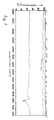
- FIGURE 1 shows transmission traces of unannealed CVD-Si samples.
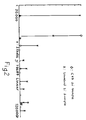
- FIGURE 2 is an X-ray diffraction scan of an unannealed CVD-Si sample.
- FIGURE 3 shows microstructure of unannealed CVD-Si.
- FIGURE 4 is a comparison of infrared transmission of annealed and unannealed CVD-Si.
- FIGURE 5 is a comparison of infrared transmission of annealed and unannealed CVD-Si.
- FIGURE 6 is an infrared transmission trace of an annealed sample of CVD-Si.
- FIGURE 7 is an infrared transmission trace of an annealed sample of CVD-Si.
- FIGURE 8 is a micrograph comparing the microstructure of (a) unannealed and (b) annealed CVD-Si.
- FIGURE 9 is a micrograph comparing the microstructure of annealed CVD-Si at two locations.
- FIGURE 10 is a comparison of X-ray diffraction of (a) unannealed and (b) annealed CVD-Si.
- FIGURE 11 is a comparison of X-ray diffraction of (a) unannealed and (b) annealed CVD-Si.
- FIGURE 12 is an infrared transmission trace of an annealed CVD-Si sample.
- FIGURE 13 is a transmission trace of an annealed sample of CVD-Si.
- FIGURE 14 is a micrograph comparing the microstructure of (a) unannealed and (b) annealed CVD- Si.
- FIGURE 15 is an infrared transmission trace of an annealed CVD-SiC sample.
- FIGURE 16 is an infrared transmission trace comparing annealed and unannealed CVD-SiC samples.
- CVD-Si particularly silicon produced by the pyrolysis reaction of SiHCl3 and H2 at deposition temperatures below about 1100°C
- the annealing substantially enhances the optical transmission properties, particularly transmission in the near infrared, of the CVD-produced silicon.
- mechanical properties are either not degraded by the annealing or degraded only slightly.
- the annealing process does not change the average values of hardness and flexural strength, within the accuracy of measurement, while the elastic modulus is decreased by only about 10% by the annealing process.
- Annealed CVD-Si samples may have Knoop hardness of between 800-1000 Kg mm ⁇ 2 and preferably above about 850 Kg mm ⁇ 2, flextural strengths of above about 20-40 Ksi and preferably above about 24 Ksi, and elastic moduli of above about 20-24 x 106 psi and preferably above about 21 x 106 psi.
- the annealed CVD-produced silicon has optical properties similar to single crystal silicon. Unlike single crystal silicon, polycrystalline, CVD-produced silicon is scalable to several meters and then can be used in a variety of window applications.
- CVD-produced silicon does not have cleavage planes and has mechanical characteristics suitable for window applications.
- the CVD-produced silicon may either be a relatively thick layer which can stand by itself as an optically-transmitting material or may be a layer on a composite optically-transmitting material.
- Optically-transmitted substrates on which silicon may be deposited by CVD and subsequently annealed include, but are not limited to SiC, Si3N4, BN, Y2O3, CaL2S4.
- Annealing times will depend upon a number of factors, such as sample thickness, whether the sample is a stand-alone sample, whether it is a layer on another substrate, and whether it is sandwiched between other materials in the annealing unit.
- the examples below show experiments in which annealing times were sufficiently long, but this is not to say that shorter annealing times might not also be successful.
- Annealed CVD-Si produced in accordance with the present invention, has attenuation coefficient at a wavelength of 3500 cm ⁇ 1 of at most 0.30 cm ⁇ 1 and lower to 0.01 cm ⁇ 1. This is a tremendous improvement relative to unannealed CVD-produced silicon which typically has an absorption coefficient of no more than about 10 cm ⁇ 1 at 3500 cm ⁇ 1.
- Optical attenuation coefficients at 3500 cm ⁇ 1 are used herein as a suitable comparison of optically transmitting materials because this is a wavelength at which infrared window materials are frequently required to exhibit good optical transmittance.
- optical transmittance across a wide range of visible and infrared wavelengths is improved by annealing CVD-produced silicon.
- Annealing is accomplished by merely heating the CVD-Si in the presence of a non-reactive atmosphere.
- the annealing may be done within the reactor where the silicon was produced by chemical vapor deposition. It appears that the annealing may be done immediately after a deposition that was performed at a somewhat lower temperature.
- silicon produced by CVD and then brought to ambient temperature may be annealed by reheating to the annealing temperature range.
- CVD-SiC is a polycrystalline material that is effectively opaque throughout the visible and infrared regions. It has been found that annealing CVD-SiC provides attenuation coefficients of at most about 4 cm ⁇ 1 at 3500 cm ⁇ 1. Although this material is not highly transmitting, the fact that it transmits light at all is a dramatic improvement over non-transmitting, unannealed CVD-SiC.
- SiC may make this material especially useful as a thin coating on infrared window material.
- Annealed CVD-Si samples may have Knoop hardness of above about 2000-2500 Kg mm ⁇ 2 and preferably above about 2500 Kg mm ⁇ 2.
- Optically-transmitted substrates on which silicon carbide may be deposited by CVD and subsequently annealed include, but are not limited to SiC, BN, Al2O3.
- Annealing temperatures for CVD-SiC are in the range of between about 1800°C and about 2600°C, preferably in the range of about 1800-2300°C, most preferably in the range of 2200°C to 2300°C. Because SiC undergoes a phase transition from its beta to its alpha form at about 2300°C, for many applications it may be advisable to anneal at below about 2300°C. Furthermore, the highest annealing temperatures may be difficult to achieve in many available annealing units.
- annealing may be done in any suitable high temperature-producing apparatus, including the deposition reactor. It is not at this time known whether it is necessary, but CVD-SiC annealing experiments have been conducted in the presence of silicon in an inert atmosphere. Silicon boils at 2355°C and has a high vapor pressure throughout the annealing temperature range of CVD-SiC, and it was felt that without the presence of external silicon vapor in the annealing atmosphere, significant amounts of silicon vaporizes from the silicon carbide. This fact was confirmed by annealing the SiC samples at 2200°C in the presence of Ar. A thick coating of carbon was detected on the annealed SiC samples.
- SiHCl3 trichlorosilane
- g and s refers to gas and solid, respectively.
- SiHCl3 is a liquid at room temperature, it was carried to the deposition area using the following two conditions: (1) Argon was used as a carrier gas and bubbled through the SiHCl3 cylinder which was maintained at about 20°C and (2) the SiHCl3 cylinder was heated to 33°C using a constant temperature bath and a mass flow controller specially designed to handle SiHCl3 was used. In this case, the mass flow controller and the associated lines were traced with a heat tape and maintained at a temperature of 36°C to prevent SiHCl3 condensation.
- the polycrystalline Si was fabricated at a substrate temperature from 950-1200°C and furnace pressure of 25-400 torr.
- the deposition was conducted in a horizontal three zone Lindberg furnace with a maximum temperature capability of 1500°C.
- the furnace support tube is made of alumina and water-cooled stainless steel injectors were used to inject a mixture of SiHCl3, H2 and Ar in the reaction zone.
- the deposition area consisted of four graphite plates, each 12 inches long and 3.5 inches wide arranged in the form of a open square box.
- the polycrystalline Si was deposited on the inside surface of this "box".
- a mould release coating was used on the graphite to facilitate recovery of Si without destroying the graphite mandrel.
- the polycrystalline Si was also successfully scaled from the horizontal research reactor to a vertical pilot plant size reactor, and Si plates 30 cm long x 25 cm wide x 0.625 cm thick were fabricated.
- SiC was produced in a low pressure CVD process to produce polycrystalline cubic ( ⁇ ) SiC based on the following chemical reaction: CH3SiCl3(g) H2,Ar T,P Sic(S) + 3HCl(g) where g and s refer to gaseous and solid species, respectively.
- the above reaction involves the pyrolysis of methyltrichlorosilane (CH3SiCl2) in excess hydrogen (H2) to produce silicon carbide (SiC), and a byproduct of the reaction is hydrogen chloride (HCl).
- FIGS 1 through 3 In FIG. 1 are shown infrared transmission traces of two samples of CVD-Si taken from two different locations in the deposition area (mandrel and baffle). The thickness of the sample was 0.067-inches. It is seen that the scattering effect in the form of reduced transmission in the near infrared region still exists. Further, the transmission of the material is quite low even in mid-infrared regions where almost theoretical transmission was obtained in previous depositions. It is not clear why there is degradation of transmission in the mid-infrared regions.
- FIG. 2 shows the x-ray diffraction scan of a CVD-Si sample taken from the mandrel. This scan was obtained from the surface of that which faced the graphite substrate. However, x-ray difffraction scans taken of other samples and at other surfaces were also similar, but are not shown here. From FIG. 2 it is seen that the material is highly oriented in the (220) direction. This result is typical for polycrystalline Si fabricated at a high deposition temperature.
- FIG. 3 shows the cross section (parallel to the growth direction) at 50 times magnification of the microstructure of a sample of CVD-Si which was polished and etched for one minute in a hot solution of 50% KOH.
- the columnar grain structure visible in this figure is typical of polycristalline Si that has been obtained in previous depositions.
- deposition Run B the process conditions used were the same as for Run A except that the substrate temperature was in the temperature range of 1030-1070°C.
- the deposition conditions for deposition Run C is not traceable at this time.
- the CVD-Si samples from the deposition Runs A, B, and C were annealed at 1300°C for five hours.
- the annealing was performed at a furnace pressure of 600 torr and with no gas flow. Examination of the annealed material indicated formation of a SiC layer on both sides of the Si sample. The presence of this layer was confirmed by the reflection measurement and the x-ray diffraction analysis. This was understandable because at 1300°C, polycrystalline Si at the sample surface reacts with carbon from the deposition setup to form SiC.
- the SiC layer was thin and easily removed by grinding the sample on both sides.
- the samples were then polished and characterized for infrared transmission, hardness, and crystal structure. These results are shown in FIGS. 4 through 10. In FIGS.
- FIG. 8 shows a comparison of microstructure, parallel to the growth direction and magnified 100 times, of annealed and unannealed samples of CVD-Si produced in deposition Run A. It is seen that the columnar growth structure so characteristic of CVD-Si (FIG. 8[a]) totally disappears after annealing, and distinct grain boundaries are visible. These grain boundaries usually appear when the microstructure is taken perpendicular to the growth direction. Thus, the appearance of these distinct grain boundaries indicates that a rearrangement of different crystallites has occurred, thereby producing a more isotropic material.
- FIG. 9 shows the microstructure taken from two different locations on the surface of annealed sample of CVD-Si produced in Run C. These micrographs were taken perpendicular to the growth direction at 100 times magnification. It is seen that the rosette pattern so characteristic of CVD-Si has totally disappeared at one location (FIG. 9[a]), while at the other location (FIG. 9[b]) it is considerably reduced. However, the average grain size has not changed due to annealing. This means that mechanical properties, such as hardness and flexural strength, should not change appreciably due to annealing.
- FIGS. 10 and 11 show a comparison of x-ray diffraction scan of sides 1 and 2, respectively, of unannealed and annealed samples of CVD-Si fabricated in deposition Run A. On both sides of the sample, it is seen that the annealing operation has changed the crystal structure from one of preferred orientation to that of more random orientation. This result is in conformity with the microstructure data as discussed above.
- Run 3 the annealing conditions of Run 2 were essentially repeated on some more samples of CVD-Si to determine if improvement in infrared transmission can be obtained in a reproducible manner. Another aim of this annealing experiment was to use relatively thicker samples such that flexural strength and elastic modulus data can be obtained.
- the samples were fabricated from CVD-Si produced in deposition Run D.
- FIGS. 12 and 13 show the infrared transmission of CVD-Si samples fabricated in deposition Run D in the wavelength range 2.5 ⁇ m - 50 ⁇ m and 1.0 ⁇ m - 1.5 ⁇ m, respectively.
- the sample thickness was 0.133-inch.
- Identical results for transmission were obtained, as before, although the CVD process conditions used to fabricate this sample were considerable different from those used previously. These results indicate that annealing process works for CVD-Si fabricated over a wide range of CVD conditions. Further, it also shows that the improvement in transmission is independent of the flow of Ar during the annealing process.
- Table 3 shows the four-point bend test results on annealed samples of CVD-Si produced in Run D. The samples were nominally polished. The length of the specimen was 50 mm. From Table 3, it is seen that the flexural strength and elastic modulus of the annealed material varies respectively from 74.6 MPa (10.8 Ksi) to 226.7 MPa (32.8 Ksi) and from 135.5 GPa (19.6 x 10⁶ psi) to 144.5 GPa (20.9 x 10⁶ psi). Because sample #3 had a large visible flaw on the surface, this data point is ignored.
- the average flexural strength and elastic modulus of the material is 162.4 ⁇ 38 MPa (23.5 ⁇ 5.5 Ksi) and 141.7 ⁇ 3.5 GPa (20.5 ⁇ 0.5 x 10⁶ psi).
- flexural strengths of 221 ⁇ 33 MPa (32 ⁇ 4.8Ksi) for polished and etched samples, 321.1 ⁇ 33 MPa (30.5 ⁇ 4.7 Ksi) for highly polished samples and 107 ⁇ 17 MPa (15.5 ⁇ 2.5 Ksi) for unpolished samples were obtained.
- the data for annealed samples which were nominally polished lie in between those of the highly polished (or polished and etched) and unpolished but unannealed samples.
- the flexural strength of the annealed samples is close to that of the unannealed samples.
- the elastic modulus of unannealed samples was measured to be 161 GPa (23.3 x 10⁶ psi) which is also close to that of the annealed samples.
- annealing of the samples does not appreciably degrade the mechanical properties of CVD-Si. This result is in conformity with the grain size data as presented above for Run 2.
- FIG. 14 shows a comparison of microstructure taken perpendicular to the growth direction at 100 times magnification of annealed and unannealed samples of CVD-Si fabricated in Run D.
- the rosette pattern showing a bimodal grain size distribution is clearly visible.
- the grain size distribution is more random.
- the Knoop hardness of the polished samples is shown in Table 5.
- the applied load was 500 grams and the indentation time was 10 seconds. It is seen the hardness of both surfaces, substrate side and as-deposited, is the same within the accuracy of measurement.
- the average Knoop hardness for an annealed sample is 2175 ⁇ 62 kg mm ⁇ 2 which is about 13% less than the average Knoop hardness of unannealed SiC (2500 kg min ⁇ 2).
- Run III it was decided to essentially repeat the conditions of Run I (SiC), except that the annealing time was changed from 5 hours to 25 hours.
- the specific CVD process conditions for these depositions E and F are listed in Table 6. It is seen that the primary difference between the two depositions was the substrate temperature and the mandrel setup.
- the SiC samples were polished and characterized for infrared transmission.
- the annealed SiC sample fabricated in Run F did not show any change in transmission, whereas the infrared transmission of annealed sample of SiC fabricated in Run E improved as shown in FIG. 16.
- the sample thickness was relatively small, i.e., 0.024-inch, a transmission of about 20% between the wavelength range 2.5-4.0 ⁇ m is quite significant.
Landscapes
- Chemical & Material Sciences (AREA)
- Organic Chemistry (AREA)
- Inorganic Chemistry (AREA)
- General Chemical & Material Sciences (AREA)
- Chemical Kinetics & Catalysis (AREA)
- Engineering & Computer Science (AREA)
- Materials Engineering (AREA)
- Mechanical Engineering (AREA)
- Metallurgy (AREA)
- Chemical Vapour Deposition (AREA)
Applications Claiming Priority (2)
| Application Number | Priority Date | Filing Date | Title |
|---|---|---|---|
| US63847391A | 1991-01-07 | 1991-01-07 | |
| US638473 | 1991-01-07 |
Publications (1)
| Publication Number | Publication Date |
|---|---|
| EP0494753A2 true EP0494753A2 (fr) | 1992-07-15 |
Family
ID=24560184
Family Applications (1)
| Application Number | Title | Priority Date | Filing Date |
|---|---|---|---|
| EP92300110A Withdrawn EP0494753A2 (fr) | 1991-01-07 | 1992-01-07 | Silicium et carbure de silicium produits par dépôt chimique en phase vapeur ayant des propriétés optiques améliorées |
Country Status (2)
| Country | Link |
|---|---|
| EP (1) | EP0494753A2 (fr) |
| CA (1) | CA2058809A1 (fr) |
Cited By (6)
| Publication number | Priority date | Publication date | Assignee | Title |
|---|---|---|---|---|
| EP0582444A1 (fr) * | 1992-07-31 | 1994-02-09 | Cvd Incorporated | Carbure de silicium ultrapur et installation de traitement à haute température des semi-conducteurs, fabriqués à partir de ce carbure |
| EP0588479A1 (fr) * | 1992-07-31 | 1994-03-23 | Cvd Incorporated | Carbure de silicium hautement polissable et à haute conductivité thermique, procédé de préparation et application |
| EP0599468A1 (fr) * | 1992-11-23 | 1994-06-01 | Cvd Incorporated | Carbure de silicium produits par dépôt chimique en phase vapeur |
| WO2005049492A1 (fr) * | 2003-11-19 | 2005-06-02 | Degussa Ag | Poudre de silicium cristalline nanoscalaire |
| EP3613704A1 (fr) * | 2014-05-07 | 2020-02-26 | Shin-Etsu Chemical Co., Ltd. | Tige de silicium polycristallin, procédé de fabrication d'une tige en silicium polycristallin et silicium monocristallin |
| CN119433720A (zh) * | 2024-11-15 | 2025-02-14 | 有研国晶辉新材料有限公司 | 一种大直径红外硅单晶及其退火方法和应用 |
-
1992
- 1992-01-06 CA CA002058809A patent/CA2058809A1/fr not_active Abandoned
- 1992-01-07 EP EP92300110A patent/EP0494753A2/fr not_active Withdrawn
Cited By (13)
| Publication number | Priority date | Publication date | Assignee | Title |
|---|---|---|---|---|
| EP0582444A1 (fr) * | 1992-07-31 | 1994-02-09 | Cvd Incorporated | Carbure de silicium ultrapur et installation de traitement à haute température des semi-conducteurs, fabriqués à partir de ce carbure |
| EP0588479A1 (fr) * | 1992-07-31 | 1994-03-23 | Cvd Incorporated | Carbure de silicium hautement polissable et à haute conductivité thermique, procédé de préparation et application |
| US5374412A (en) * | 1992-07-31 | 1994-12-20 | Cvd, Inc. | Highly polishable, highly thermally conductive silicon carbide |
| EP0599468A1 (fr) * | 1992-11-23 | 1994-06-01 | Cvd Incorporated | Carbure de silicium produits par dépôt chimique en phase vapeur |
| KR100769442B1 (ko) * | 2003-11-19 | 2007-10-22 | 데구사 게엠베하 | 나노스케일 결정성 실리콘 분말 |
| JP2007511460A (ja) * | 2003-11-19 | 2007-05-10 | デグサ ゲーエムベーハー | ナノスケールの結晶質シリコン粉末 |
| WO2005049492A1 (fr) * | 2003-11-19 | 2005-06-02 | Degussa Ag | Poudre de silicium cristalline nanoscalaire |
| CN100404416C (zh) * | 2003-11-19 | 2008-07-23 | 德古萨股份公司 | 纳米级晶体硅粉末 |
| US7776304B2 (en) | 2003-11-19 | 2010-08-17 | Evonik Degussa Gmbh | Nanoscale crystalline silicon powder |
| US7927570B2 (en) | 2003-11-19 | 2011-04-19 | Evonik Degussa Gmbh | Nanoscale crystalline silicon powder |
| US8043593B2 (en) | 2003-11-19 | 2011-10-25 | Evonik Degussa Gmbh | Nanoscale crystalline silicon powder |
| EP3613704A1 (fr) * | 2014-05-07 | 2020-02-26 | Shin-Etsu Chemical Co., Ltd. | Tige de silicium polycristallin, procédé de fabrication d'une tige en silicium polycristallin et silicium monocristallin |
| CN119433720A (zh) * | 2024-11-15 | 2025-02-14 | 有研国晶辉新材料有限公司 | 一种大直径红外硅单晶及其退火方法和应用 |
Also Published As
| Publication number | Publication date |
|---|---|
| CA2058809A1 (fr) | 1992-07-08 |
Similar Documents
| Publication | Publication Date | Title |
|---|---|---|
| CA2104411C (fr) | Carbure de silicium par deposition-production de vapeur chimique, a proprietes ameliorees | |
| US9023306B2 (en) | Ultratough single crystal boron-doped diamond | |
| CA2027171C (fr) | Methode de deposition en phase vapeur pour reproduire le fini ou la configuration de structures prefaconnees | |
| HK1003034B (en) | Chemical-vapor-deposition-produced silicon carbide | |
| Cheng et al. | Transparent highly oriented 3C-SiC bulks by halide laser CVD | |
| Biesuz et al. | First synthesis of silicon nanocrystals in amorphous silicon nitride from a preceramic polymer | |
| Xu et al. | Morphology and growth mechanism of silicon carbide chemical vapor deposited at low temperatures and normal atmosphere | |
| Saito et al. | Diamond-like carbon films prepared from CH4-H2-H2O mixed gas using a microwave plasma | |
| RU2363067C1 (ru) | Способ изготовления изделия, содержащего кремниевую подложку с пленкой из карбида кремния на ее поверхности | |
| Baraton et al. | Nanometric boron nitride powders: laser synthesis, characterization and FT-IR surface study | |
| US6083561A (en) | Low scatter, high quality water clear zinc sulfide | |
| US4772304A (en) | Transparent BN-type ceramic material and method of producing the same | |
| CA2058809A1 (fr) | Depot chimique en phase vapeur de silicium et de carbure de silicium aux proprietes optiques ameliorees | |
| RU2286616C2 (ru) | Способ изготовления изделия, содержащего кремниевую подложку с пленкой из карбида кремния на ее поверхности | |
| CA2042269A1 (fr) | Articles d'optique proteges contre le rayonnement et obtenus a partir d'un diamant forme d'un cristal unique de grande purete isotopique | |
| Fredriksson et al. | Chemical vapour deposition of TiO and Ti2O3 from TiCl4/H2/CO2 gas mixtures | |
| KR940005278B1 (ko) | X선 마스크용 멤브레인 및 제조법 | |
| Goela et al. | Postdeposition Process for Improving Optical Properties of Chemical‐Vapor‐Deposited Silicon | |
| Park et al. | First Approach to an AlSb Layer from the Single‐Source Precursors [Et2AlSb (SiMe3) 2] 2 and [iBu2AlSb (SiMe3) 2] 2 | |
| WO2021034214A1 (fr) | Article comportant un revêtement en carbure de silicium et procédé de production d'article comportant un revêtement en carbure de silicium | |
| Grannen et al. | The growth of silicon nitride crystalline films using microwave plasma enhanced chemical vapor deposition | |
| Biswas et al. | Fabrication of IR transparent zin c sulphide plate by chemical vapour deposition (CVD) | |
| Tanzilli et al. | Processing Research on Chemically Vapor Deposited Silicon Nitride. | |
| Feldman et al. | Diamond, a potentially new optical coating material | |
| Devi et al. | Boron nitride thin films on Si (100) by metal organic chemical vapour deposition |
Legal Events
| Date | Code | Title | Description |
|---|---|---|---|
| PUAI | Public reference made under article 153(3) epc to a published international application that has entered the european phase |
Free format text: ORIGINAL CODE: 0009012 |
|
| AK | Designated contracting states |
Kind code of ref document: A2 Designated state(s): CH DE FR GB IT LI |
|
| 18W | Application withdrawn |
Withdrawal date: 19920924 |
|
| R18W | Application withdrawn (corrected) |
Effective date: 19920924 |