EP0494766A2 - Lasers à semi-conducteurs - Google Patents
Lasers à semi-conducteurs Download PDFInfo
- Publication number
- EP0494766A2 EP0494766A2 EP92300143A EP92300143A EP0494766A2 EP 0494766 A2 EP0494766 A2 EP 0494766A2 EP 92300143 A EP92300143 A EP 92300143A EP 92300143 A EP92300143 A EP 92300143A EP 0494766 A2 EP0494766 A2 EP 0494766A2
- Authority
- EP
- European Patent Office
- Prior art keywords
- layer
- semiconductor layers
- groove
- quantum
- quantum wire
- Prior art date
- Legal status (The legal status is an assumption and is not a legal conclusion. Google has not performed a legal analysis and makes no representation as to the accuracy of the status listed.)
- Granted
Links
Images




Classifications
-
- B—PERFORMING OPERATIONS; TRANSPORTING
- B82—NANOTECHNOLOGY
- B82Y—SPECIFIC USES OR APPLICATIONS OF NANOSTRUCTURES; MEASUREMENT OR ANALYSIS OF NANOSTRUCTURES; MANUFACTURE OR TREATMENT OF NANOSTRUCTURES
- B82Y20/00—Nanooptics, e.g. quantum optics or photonic crystals
-
- H—ELECTRICITY
- H01—ELECTRIC ELEMENTS
- H01S—DEVICES USING THE PROCESS OF LIGHT AMPLIFICATION BY STIMULATED EMISSION OF RADIATION [LASER] TO AMPLIFY OR GENERATE LIGHT; DEVICES USING STIMULATED EMISSION OF ELECTROMAGNETIC RADIATION IN WAVE RANGES OTHER THAN OPTICAL
- H01S5/00—Semiconductor lasers
- H01S5/10—Construction or shape of the optical resonator, e.g. extended or external cavity, coupled cavities, bent-guide, varying width, thickness or composition of the active region
- H01S5/12—Construction or shape of the optical resonator, e.g. extended or external cavity, coupled cavities, bent-guide, varying width, thickness or composition of the active region the resonator having a periodic structure, e.g. in distributed feedback [DFB] lasers
- H01S5/1228—DFB lasers with a complex coupled grating, e.g. gain or loss coupling
-
- H—ELECTRICITY
- H01—ELECTRIC ELEMENTS
- H01S—DEVICES USING THE PROCESS OF LIGHT AMPLIFICATION BY STIMULATED EMISSION OF RADIATION [LASER] TO AMPLIFY OR GENERATE LIGHT; DEVICES USING STIMULATED EMISSION OF ELECTROMAGNETIC RADIATION IN WAVE RANGES OTHER THAN OPTICAL
- H01S5/00—Semiconductor lasers
- H01S5/20—Structure or shape of the semiconductor body to guide the optical wave ; Confining structures perpendicular to the optical axis, e.g. index or gain guiding, stripe geometry, broad area lasers, gain tailoring, transverse or lateral reflectors, special cladding structures, MQW barrier reflection layers
-
- H—ELECTRICITY
- H01—ELECTRIC ELEMENTS
- H01S—DEVICES USING THE PROCESS OF LIGHT AMPLIFICATION BY STIMULATED EMISSION OF RADIATION [LASER] TO AMPLIFY OR GENERATE LIGHT; DEVICES USING STIMULATED EMISSION OF ELECTROMAGNETIC RADIATION IN WAVE RANGES OTHER THAN OPTICAL
- H01S5/00—Semiconductor lasers
- H01S5/30—Structure or shape of the active region; Materials used for the active region
- H01S5/34—Structure or shape of the active region; Materials used for the active region comprising quantum well or superlattice structures, e.g. single quantum well [SQW] lasers, multiple quantum well [MQW] lasers or graded index separate confinement heterostructure [GRINSCH] lasers
- H01S5/341—Structures having reduced dimensionality, e.g. quantum wires
-
- H—ELECTRICITY
- H01—ELECTRIC ELEMENTS
- H01S—DEVICES USING THE PROCESS OF LIGHT AMPLIFICATION BY STIMULATED EMISSION OF RADIATION [LASER] TO AMPLIFY OR GENERATE LIGHT; DEVICES USING STIMULATED EMISSION OF ELECTROMAGNETIC RADIATION IN WAVE RANGES OTHER THAN OPTICAL
- H01S5/00—Semiconductor lasers
- H01S5/40—Arrangement of two or more semiconductor lasers, not provided for in groups H01S5/02 - H01S5/30
- H01S5/4025—Array arrangements, e.g. constituted by discrete laser diodes or laser bar
- H01S5/4031—Edge-emitting structures
- H01S5/4043—Edge-emitting structures with vertically stacked active layers
- H01S5/405—Two-dimensional arrays
-
- H—ELECTRICITY
- H01—ELECTRIC ELEMENTS
- H01S—DEVICES USING THE PROCESS OF LIGHT AMPLIFICATION BY STIMULATED EMISSION OF RADIATION [LASER] TO AMPLIFY OR GENERATE LIGHT; DEVICES USING STIMULATED EMISSION OF ELECTROMAGNETIC RADIATION IN WAVE RANGES OTHER THAN OPTICAL
- H01S5/00—Semiconductor lasers
- H01S5/20—Structure or shape of the semiconductor body to guide the optical wave ; Confining structures perpendicular to the optical axis, e.g. index or gain guiding, stripe geometry, broad area lasers, gain tailoring, transverse or lateral reflectors, special cladding structures, MQW barrier reflection layers
- H01S5/2054—Methods of obtaining the confinement
- H01S5/2059—Methods of obtaining the confinement by means of particular conductivity zones, e.g. obtained by particle bombardment or diffusion
-
- H—ELECTRICITY
- H01—ELECTRIC ELEMENTS
- H01S—DEVICES USING THE PROCESS OF LIGHT AMPLIFICATION BY STIMULATED EMISSION OF RADIATION [LASER] TO AMPLIFY OR GENERATE LIGHT; DEVICES USING STIMULATED EMISSION OF ELECTROMAGNETIC RADIATION IN WAVE RANGES OTHER THAN OPTICAL
- H01S5/00—Semiconductor lasers
- H01S5/20—Structure or shape of the semiconductor body to guide the optical wave ; Confining structures perpendicular to the optical axis, e.g. index or gain guiding, stripe geometry, broad area lasers, gain tailoring, transverse or lateral reflectors, special cladding structures, MQW barrier reflection layers
- H01S5/2054—Methods of obtaining the confinement
- H01S5/2059—Methods of obtaining the confinement by means of particular conductivity zones, e.g. obtained by particle bombardment or diffusion
- H01S5/2068—Methods of obtaining the confinement by means of particular conductivity zones, e.g. obtained by particle bombardment or diffusion obtained by radiation treatment or annealing
-
- H—ELECTRICITY
- H01—ELECTRIC ELEMENTS
- H01S—DEVICES USING THE PROCESS OF LIGHT AMPLIFICATION BY STIMULATED EMISSION OF RADIATION [LASER] TO AMPLIFY OR GENERATE LIGHT; DEVICES USING STIMULATED EMISSION OF ELECTROMAGNETIC RADIATION IN WAVE RANGES OTHER THAN OPTICAL
- H01S5/00—Semiconductor lasers
- H01S5/20—Structure or shape of the semiconductor body to guide the optical wave ; Confining structures perpendicular to the optical axis, e.g. index or gain guiding, stripe geometry, broad area lasers, gain tailoring, transverse or lateral reflectors, special cladding structures, MQW barrier reflection layers
- H01S5/22—Structure or shape of the semiconductor body to guide the optical wave ; Confining structures perpendicular to the optical axis, e.g. index or gain guiding, stripe geometry, broad area lasers, gain tailoring, transverse or lateral reflectors, special cladding structures, MQW barrier reflection layers having a ridge or stripe structure
- H01S5/223—Buried stripe structure
- H01S5/2232—Buried stripe structure with inner confining structure between the active layer and the lower electrode
- H01S5/2234—Buried stripe structure with inner confining structure between the active layer and the lower electrode having a structured substrate surface
-
- H—ELECTRICITY
- H01—ELECTRIC ELEMENTS
- H01S—DEVICES USING THE PROCESS OF LIGHT AMPLIFICATION BY STIMULATED EMISSION OF RADIATION [LASER] TO AMPLIFY OR GENERATE LIGHT; DEVICES USING STIMULATED EMISSION OF ELECTROMAGNETIC RADIATION IN WAVE RANGES OTHER THAN OPTICAL
- H01S5/00—Semiconductor lasers
- H01S5/20—Structure or shape of the semiconductor body to guide the optical wave ; Confining structures perpendicular to the optical axis, e.g. index or gain guiding, stripe geometry, broad area lasers, gain tailoring, transverse or lateral reflectors, special cladding structures, MQW barrier reflection layers
- H01S5/22—Structure or shape of the semiconductor body to guide the optical wave ; Confining structures perpendicular to the optical axis, e.g. index or gain guiding, stripe geometry, broad area lasers, gain tailoring, transverse or lateral reflectors, special cladding structures, MQW barrier reflection layers having a ridge or stripe structure
- H01S5/223—Buried stripe structure
- H01S5/2232—Buried stripe structure with inner confining structure between the active layer and the lower electrode
- H01S5/2234—Buried stripe structure with inner confining structure between the active layer and the lower electrode having a structured substrate surface
- H01S5/2235—Buried stripe structure with inner confining structure between the active layer and the lower electrode having a structured substrate surface with a protrusion
-
- H—ELECTRICITY
- H01—ELECTRIC ELEMENTS
- H01S—DEVICES USING THE PROCESS OF LIGHT AMPLIFICATION BY STIMULATED EMISSION OF RADIATION [LASER] TO AMPLIFY OR GENERATE LIGHT; DEVICES USING STIMULATED EMISSION OF ELECTROMAGNETIC RADIATION IN WAVE RANGES OTHER THAN OPTICAL
- H01S5/00—Semiconductor lasers
- H01S5/20—Structure or shape of the semiconductor body to guide the optical wave ; Confining structures perpendicular to the optical axis, e.g. index or gain guiding, stripe geometry, broad area lasers, gain tailoring, transverse or lateral reflectors, special cladding structures, MQW barrier reflection layers
- H01S5/22—Structure or shape of the semiconductor body to guide the optical wave ; Confining structures perpendicular to the optical axis, e.g. index or gain guiding, stripe geometry, broad area lasers, gain tailoring, transverse or lateral reflectors, special cladding structures, MQW barrier reflection layers having a ridge or stripe structure
- H01S5/223—Buried stripe structure
- H01S5/2237—Buried stripe structure with a non-planar active layer
-
- H—ELECTRICITY
- H01—ELECTRIC ELEMENTS
- H01S—DEVICES USING THE PROCESS OF LIGHT AMPLIFICATION BY STIMULATED EMISSION OF RADIATION [LASER] TO AMPLIFY OR GENERATE LIGHT; DEVICES USING STIMULATED EMISSION OF ELECTROMAGNETIC RADIATION IN WAVE RANGES OTHER THAN OPTICAL
- H01S5/00—Semiconductor lasers
- H01S5/20—Structure or shape of the semiconductor body to guide the optical wave ; Confining structures perpendicular to the optical axis, e.g. index or gain guiding, stripe geometry, broad area lasers, gain tailoring, transverse or lateral reflectors, special cladding structures, MQW barrier reflection layers
- H01S5/24—Structure or shape of the semiconductor body to guide the optical wave ; Confining structures perpendicular to the optical axis, e.g. index or gain guiding, stripe geometry, broad area lasers, gain tailoring, transverse or lateral reflectors, special cladding structures, MQW barrier reflection layers having a grooved structure, e.g. V-grooved, crescent active layer in groove, VSIS laser
-
- H—ELECTRICITY
- H01—ELECTRIC ELEMENTS
- H01S—DEVICES USING THE PROCESS OF LIGHT AMPLIFICATION BY STIMULATED EMISSION OF RADIATION [LASER] TO AMPLIFY OR GENERATE LIGHT; DEVICES USING STIMULATED EMISSION OF ELECTROMAGNETIC RADIATION IN WAVE RANGES OTHER THAN OPTICAL
- H01S5/00—Semiconductor lasers
- H01S5/40—Arrangement of two or more semiconductor lasers, not provided for in groups H01S5/02 - H01S5/30
- H01S5/4025—Array arrangements, e.g. constituted by discrete laser diodes or laser bar
- H01S5/4031—Edge-emitting structures
- H01S5/4043—Edge-emitting structures with vertically stacked active layers
Definitions
- the present invention relates generally to semiconductor structures and more particularly to semiconductor laser structures having quantum wires fabricated employing in situ photo-induced modifications to compound semiconductor films during epitaxial growth.
- Quantum wires in semiconductors are regions in which the charge carriers are quantum confined in the two dimensions orthogonal to the axis of the wire. Quantum effects in GaAs layers are most strong when the thickness is less than 50 nm. A quantum wire will still be useful if only one of its dimensions is less than 50 nm. For GaAs this typically means a region for the quantum wire in a semiconductor smaller than about 50 nm by 100 nm.
- a quantum well layer such as GaAs has been grown to fill in a previously etched V-shaped groove in the substrate to form a laser structure.
- Kapon et al. "Quantum Well Lasers Using Patterned Growth", 1988 IEEE Lasers and Electro-Optics Society Annual Meeting , Paper OE-2, Kapon et al., " Patterned quantum well semiconductor injection laser grown by molecular beam epitaxy” , Appl. Phys. Letters 52, 607 (1988).
- the resulting quantum well layer is thinner on the sides of the groove than near the vertex but the thin sidewall quantum layer is still present.
- carrier recombination and lasing in this structure may occur in the quantum well regions on the sides of the groove since these regions are larger and therefore provide more gain than the smaller vertex region.
- This invention addresses the elimination of the sidewall growth.
- patterning may be achieved by quasi- in situ thermal processing wherein thermal etching is employed to remove GaAs selectively.
- thermal etching is employed to remove GaAs selectively.
- a n-GaAs layer over a p-AlGaAs layer is first selectively chemically etched in a particular region, followed by thermal etching to remove the remaining thin GaAs left from chemical etching before proceeding with regrowth of the p-AlGaAs layer. This forms a buried reverse biased current confinement mechanism in a double heterostructure laser.
- a GaAs/AlGaAs heterostructure partially masked by a metallic film is thermally etched in an anisotropic manner illustrating submicron capabilities for device fabrication.
- A. C. Warren et al "Masked, Anisotropic Thermal Etching and Regrowth for In Situ Patterning of Compound Semiconductors", Applied Physics Letters , Vol. 51 (22), pp. 1818-1820, November 30, 1987.
- AlGaAs masking layers are recognized as an etch stop to provide for the desired geometric configuration in thermally etched GaAs, although it is also known that, given the proper desorption parameters, AlGaAs may also be thermally etched at higher temperatures with different attending ambient conditions vis-a-vis GaAs.
- MOCVD metalorganic chemical vapor deposition
- in situ removal or thinning of portions or all of selected regions of deposited films is brought about by a technique employing an irradiation energy source directed to a spot or region of exposure on the growth surface of a substrate or support in a deposition system, e.g., MBE or MOCVD system.
- a deposition system e.g., MBE or MOCVD system.
- the invention herein is directed to the employment of this technique in fabricating in situ quantum wires in semiconductor laser structures wherein induced evaporation enhancement purely removes or prevents the continued growth of the epitaxially deposited materials in selected regions at the growth surface without the need or introduction of masking or chemical etching processes.
- the application of this technique, as particularly described here provides the opportunity to produce in situ current reverse bias confinement configurations and impurity induced waveguides which effectively channel current to designated regions of the semiconductor laser structure by means of patterned desorption of layer induced evaporation enhancement.
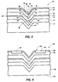
- semiconductor laser structure 10 having a single quantum wire and fabricated using MOCVD processing as described in US-A-4,962,057.
- Semiconductor laser structure 10 includes a substrate 12 of n-GaAs with an appropriate buffer layer upon which is a groove 14.
- the groove can be fabricated in the cladding layer by chemical etching, reactive ion etching, ion milling or other means.
- the groove can also be fabricated by a tightly focussed beam scanned across the surface of the cladding layer with changing dwell time, a process described in US-A-4,962,057.
- the groove should be as narrow as possible. However, the width and depth of the groove will depend upon the process used to fabricate it. It is desirable to form grooves which are deeper than their width with resulting sidewall angles greater than 45 degrees. For example, chemical etching and beam desorption may form grooves in a V-shape with an angular separation of the opposing sidewalls of 70.5 degrees. Reactive ion etching or ion milling may form grooves with widely variable sidewall angles and even grooves with vertical sidewalls. Similarly, etching may form grooves with sidewalls culminating in flat bases.
- the optimum sidewall angle of the groove will depend upon the particulars of the semiconductor laser structure. More gradually sloping sidewalls will aid in attaining subsequent high quality epitaxy without voids in the vertex region, and will tend to reflect impinging desorbing radiation out of the groove, thus preventing a concentration of the radiation within the groove. Steeper sidewalls, on the other hand, have the advantages of a smaller dimension at the vertex of the groove for formation of the quantum scale wire, greater redeposition of desorbed material which favors retaining the appropriate amount of material at the vertex and greater shadowing effect as described below.
- the groove 14 is V-shaped with opposing acute-angled sidewalls 16 and 18 culminating in vertex 20.
- the groove can be from 10 nm to 2.5 ⁇ m deep.
- the outer cladding layer 22 has a V-shaped groove 26 with sidewalls 28 and 30 and vertex 32, parallel to the groove 14 with its sidewalls 16 and 18 in the substrate 12.
- Inner confinement layer 24 has a V-shaped groove 34 with sidewalls 36 and 38 and vertex 40, parallel to the grooves and sidewalls of the outer cladding layer and the substrate.
- the grooves are self-aligning since the subsequently deposited layers of uniform thickness will follow the contour of the previously deposited layers.
- the substrate temperature is increased to about 825 °C and a laser beam or combination laser beam is focussed on the surface of quantum well layer 42 either orthogonally or, as indicated by lines 56 in Figure 2, at an angle near normal incidence to the sidewalls for a period of time sufficient to evaporate quantum well layer 42 thermally at sidewalls 44 and 46 to the sidewalls 36 and 38 of inner cladding layer 24 at a rate of 0.1 nm.
- the temperature at the illuminated portion of the quantum well layer 42 during the evaporation process may be about 1000°C to 1030°C.
- the areas of quantum well layer 42 along the sidewalls 44 and 46 are desorbed down to the interface with inner confinement layer 24 resulting in a crescent shaped quantum wire 58 forming in the vertex 40 of the groove 34 of the inner confinement layer 24.
- Orienting the polarization of the laser beam parallel to the plane of incidence which, for example, can be perpendicular to the quantum wire, aids in the removal of undesired material from the surface and sidewalls of the groove, since light will be most effectively coupled into the material.
- the Al y Ga 1-y As of the confinement layer 24 functions as a desorption stop to the optically induced desorption because Al y Ga 1-y As where y ⁇ 0.15 is much more difficult to desorb according to this process as compared to the desorption of the GaAs of the quantum well layer 42.
- the operating temperature for AlGaAs will be higher than that for GaAs because the Al content in AlGaAs causes a slower evaporation rate since GaAs has a higher vapor pressure than AlGaAs.
- the incident angle of the laser beam 56 can also be adjusted to shadow the vertex and concentrate illumination on the sidewalls as shown in Figure 2.
- the desorption of the quantum well layer in the shadowed vertex region will proceed more slowly than it would in the presence of illumination since any photochemical desorption will be reduced or eliminated and the vertex region will be cooler than its surrounding sidewalls. Both effects will enhance the lateral selectivity of the desorption.
- the optical process should be highly reproducible because exposure time and illumination intensity can be accurately controlled.
- US-A-4,962,057 allows growth of the quantum well layer to be performed at a temperature that optimizes the quality of the layer for laser desorption.
- the desorption can subsequently be accomplished at a base temperature conducive to the preferential thinning of the sidewalls relative to the vertex region.
- the laser approach to the desorption is preferable to the simple raising of the temperature of the substrate to induce desorption because the intensity of the optical illumination allows for faster control of the semiconductor temperature, shorter desorption times and less time spent at high undesired temperatures. All of these factors greatly enhance the reproducibility of the process using optical illumination.
- a crescent shaped quantum wire 58 has formed in vertex 40 of the groove 34 of the inner confinement layer 24, thinned quantum well layers 60 and 62 remain on the mesa levels of inner confinement layer 24 and the quantum well layer no longer exists on the sidewalls 36 and 38 of the groove.
- Epitaxial growth of semiconductor laser structure 10 is then continued with the growth of a second inner confinement layer 64 of p-Al y Ga 1-y As and second outer cladding layer 66 of p-Al A Ga 1-A As where x ⁇ or ⁇ A ⁇ y and cap layer 68 of p+-GaAs.
- Each of these layers provides a uniform thickness on top of the previous semiconductor layers.
- the thinned quantum well layers 60 and 62 on the mesa levels do not lase because current is confined to the quantum wire.
- the layers on the mesas may be removed by the desorbing laser beam.
- the inner confinement layer 64 has a V-shaped groove 70 with sidewalls 72 and 74 and vertex 76, parallel to the grooves and sidewalls in the inner confinement layer 24, outer cladding layer 22 and the substrate 12.
- Outer cladding layer 66 has a V-shaped groove 78 with sidewalls 80 and 82 and vertex 84, parallel to the grooves and sidewalls of the inner confinement layers 64 and 24, outer cladding layer 22 and the substrate 12.
- Cap layer 68 has a V-shaped groove 86 with sidewalls 88 and 90 and vertex 92, parallel to the grooves and sidewalls of the outer cladding layer 66, inner confinement layers 64 and 24, outer cladding layer 22 and the substrate 12.
- the grooves are self-aligning since the subsequently deposited layers of uniform thickness will follow the contour of the previously deposited layers.
- the GaAs of the quantum well layer grows faster at the bottom vertex of the groove while the AlGaAs of the cladding layer grows faster on the sidewalls of the groove, thus the groove is reformed in the AlGaAs cladding layer after each GaAs quantum wire crescent.
- the inner confinement layer 64, the outer cladding layer 66 and the cap layer 68 are not required to follow the grooves and sidewalls of the lower layers.
- the quantum well layer 42 and resulting quantum wire 58 can be of low bandgap semiconductor material with the adjacent inner confinement layers 24 and 64 of high bandgap semiconductor material to reduce carrier and radiation lossses and to localize carriers to adjacent quantum wires in multiple quantum wire semiconductor laser structures described below.
- Standard chemical etching means or other metallization techniques are employed to form a p-contact on the cap layer 12 and a n-contact on the substrate 68 (not shown).
- the p-cladding layer 66 and the n-cladding layer 22 form a p-n junction with the quantum wire 58 therebetween.
- Current is injected between the p-contact and the n-contact to forward-bias the p-n junction of p-cladding layer 66 and the n-cladding layer 22 to cause the active quantum wire 58 to emit coherent light.
- US-A-4,962,057 permit the full in situ processing of a quantum wire semiconductor laser structure 10 without removal of the structure from the MOCVD reactor or movement or masking of the structure in the reactor.
- the quantum wire semiconductor laser structure 94 is of identical structure to the quantum wire semiconductor laser structure 10 of Figure 3, except that a current confinement stripe is formed by proton bombardment or ion implantation regions 96 through the cap layer 100 of p-GaAs and into the second outer cladding layer 98 of p-AlGaAs. Appropriate contact metals are then applied to the outer surface 102 of the cap layer 100 and outer surface 104 of the substrate 106.
- the quantum wire semiconductor laser structure 108 is of identical structure to the quantum wire semiconductor laser structure 10 of Figure 3, except that the substrate 110 of n-GaAs is flat and the groove 112 is fabricated in the fisrt outer cladding layer 114 of n-Al x Ga 1-x As.
- the groove can be fabricated by a tightly focussed beam scanned across the surface of the outer cladding layer with changing dwell time.
- the groove 112 is V-shaped with opposing acute-angled sidewalls 116 and 118 culminating in a vertex 120.
- the quantum wire semiconductor laser 108 is fabricated in the identical fashion as the quantum wire semiconductor laser 10 as shown in Figures 1 to 3.
- a first inner confinement layer 122 of n-Al y Ga 1-y As where x>y is epitaxially deposited on the outer cladding layer 112 following the contour of the groove.
- Epitaxial growth is then continued with the growth of a second inner confinement layer 128 of p-Al y Ga 1-y As and second outer cladding layer 130 of p-Al A Ga 1-A As where x ⁇ or ⁇ A ⁇ y and cap layer 132 of p+-GaAs.
- Figures 6, 7 and 8 disclose a quantum wire semiconductor laser structure including a reverse bias junction in the cladding region of the laser for purposes of current confinement and a buried quantum wire, both of which are formed in situ during epitaxial growth employing induced evaporation enhancement.
- reverse bias junction quantum wire semiconductor laser 134 includes a substrate 136 of n-GaAs upon which is a V-shaped groove 138. Upon the substrate and groove is epitaxially deposited a first outer cladding layer 140 of n-Al x Ga 1-x As forming a groove 142, first inner confinement layer 144 of n-Al y Ga 1-y As where x>y forming a groove 146 and an active quantum well layer of GaAs.
- epitaxial growth is temporarily discontinued and a quantum wire 148 in the vertex of the groove and thinned quantum layers 150 and 152 on the mesa of the semiconductor layers are fabricated by a focused laser beam locally desorbing the epitaxial grown quantum well layer.
- Epitaxial growth is then continued with the growth of second inner confinement layer 154 of p-Al y Ga 1-y As forming a groove 156 and second outer cladding layer 158 of p-Al A Ga 1-A As where x ⁇ or ⁇ A ⁇ y forming a V-shaped groove 160 with opposing acute angled sidewalls 162 and 164 meeting at vertex 166, above and aligned with the grooves of the previous layers.
- the growth of the semiconductor layers is temporarily discontinued, a laser beam is focussed on the central region of the doped quantum well layer above the V-shaped grooves 160, 156, 146, 142 and 138 and quantum wire 148 to provide a temperature gradient sufficient to induce the desorption of a strip in the doped quantum well layer down to the interface with outer cladding layer 158 at sidewalls 162 and 164 forming a current channel 168 in the quantum well layer.
- the Al A Ga 1-A As of the outer cladding layer 158 functions as a desorption stop to the optically patterned desorption at the interface because AlGaAs is more difficult to desorb compared to the n-doped GaAs quantum well layer.
- GaAs is desorbed at channel 168 at a rate of about 0.03 nanometers per second with a temperature of approximately 1030°C from a spot focussed to a diameter slightly larger than the width of the groove 156.
- the n-GaAs is desorbed from the sidewalls more rapidly than from the flat mesa top so that channel 168 is completely opened.
- the doped quantum well layer remaining on the mesas of the outer confinement layer forms a reverse bias junction configuration or blocking layer 170.
- Epitaxial growth is continued with the growth of outer cladding layer 172 of p-Al B Ga 1-B As where x ⁇ A ⁇ or ⁇ B>y, followed by the growth of cap layer 174 of Mg doped p+-GaAs.
- Standard chemical etching means or other metallization techniques as are known in the art are employed to form a p-contact on the cap layer 174 and a n-contact on the substrate 136 (not shown).
- the p-cladding layer 158 and the n-cladding layer 140 form a p-n junction with the quantum wire 148 therebetween.
- Current is injected between the p-contact and the n-contact to forward-bias the p-n junction of p-cladding layer 158 and the n-cladding layer 140 to cause the active quantum wire 148 to emit coherent light.
- the reverse bias junction 170 in combination with the adjacent cladding layers 158 and 172 can function as an optical waveguide which is self-aligned with the current channel 168 and quantum wire active region 148.
- layers 158 and 172 may both be comprised of Al 0.8 Ga 0.2 As.
- This optical waveguide structure with the reverse bias junction 170 provides for an index guide that has emphasis on lateral waveguiding properties.
- an antiguiding optical waveguide structure can be created in conjunction with reverse biased junction configuration 170, e.g., layer 158 may be Al 0.8 Ga 0.2 As and layer 172 may be Al 0.1 Ga 0.9 As.
- This antiguiding structure enables high power operation in a stable mode by spreading optical power across a large lateral dimension at the output facet of the laser structure.
- the reverse bias junction quantum wire semiconductor laser 176 is identical in structure to laser 134 of Figure 6 except that the current channel and reverse bias junction are on the n-side of the quantum wire.
- the reverse bias junction quantum wire semiconductor laser 176 includes a substrate 178 of n-GaAs upon which is a V-shaped groove 180. Upon the substrate and groove is epitaxially deposited an outer cladding layer 182 of n-Al x Ga 1-x As forming a groove 184 and then a p-type doped quantum well layer of p-GaAs heavy doped, for example with Mg or C.
- the growth of the semiconductor layers is temporarily discontinued, a laser beam is focussed on the central region of the doped quantum well layer above the V-shaped grooves 184 and 180 to provide a temperature gradient sufficient to induce the desorption of a strip in the doped quantum well layer down to the interface with the cladding layer 182 forming a current channel 186 in the quantum well layer.
- the doped quantum well layer remaining on the mesas of the outer cladding layer forms a reverse bias junction configuration or blocking layer 188.
- Epitaxial growth is continued with the epitaxial growth of first outer cladding layer 190 of n-Al w Ga 1-w As where w ⁇ x and first inner confinement layer 192 of n-Al z Ga 1-z As where x ⁇ w>z and thence quantum wire 194 of GaAs and thinned quantum well layers 196 of GaAs and thence the sequential growth of a second inner confinement layer 198 of p-Al y Ga 1-y As and second outer cladding layer 200 of p-Al A Ga 1-A As where x ⁇ or ⁇ A>y and cap layer 202 of p+-GaAs.
- composition of the adjacent cladding layers with the reverse bias junction of Figure 7 may provide an optical waveguide of either an index guide or an antiguiding structure.
- the reverse bias junction quantum wire semiconductor laser 204 is identical in structure to laser 134 of Figure 6 and laser 176 of Figure 7 except that the current channel and reverse bias junction are on both the n- and p-sides of the quantum wire.
- the reverse bias junction quantum wire semiconductor laser 204 has a n-side reverse bias junction 206 and corresponding current channel 208, a quantum wire 210, and a p-side reverse bias junction 212 and corresponding current channel 214.
- the blocking layer and current channel in a reverse bias junction quantum wire semiconductor laser can be located between other layers in the semiconductor.
- Figures 6, 7 and 8 are merely illustrative examples.
- Figure 9 discloses a quantum wire semiconductor laser structure including an optical waveguide and a buried quantum wire, both of which are formed in situ during epitaxial growth employing induced evaporation enhancement.
- the semiconductor laser structure 216 includes a substrate 218 of n-GaAs, with a V-shaped groove 220, upon which is epitaxially deposited a first outer cladding layer 222 of n-Al x Ga 1-x As, forming a groove 224; a first inner confinement layer 226 of n-Al y Ga 1-y As where x>y, forming a groove 228; an active quantum wire 230 of GaAs within the groove 228, a second inner confinement layer 232 of p-Al y Ga 1-y As, forming a groove 234 and an impurity source layer 236 comprising n-GaAs heavily doped, for example, with Si or Se at a concentration in excess of 1019/cm3 or up to a point of saturated concentration of the Si or Se elemental constituent in GaAs.
- Impurity source layer 236 is shown thick broken lines in Figure 9 to emphasize its higher dopant property.
- Impurity source layer 236 may be very thin, i.e. of quantum well size such as 7.5 nm, and may also be, alternatively alone or in combination therewith, a Si or Se spike comprising one or more atomic monolayers thick.
- impurity source layer 2366 After the growth of impurity source layer 236, epitaxial growth is temporarily discontinued, the temperature of the substrate is increased if necessary, the metalorganic sources are vented, a 1% arsine/hydrogen mixture is introduced into the MOCVD chamber and a laser beam is focussed to the central region of impurity source layer 236 to provide a temperature gradient sufficient to induce the desorption of a linear stripe in the source layer 236 down to the interface with second inner confinement layer 232 forming a channel in layer 236.
- the Al y Ga 1-y As of confinement layer 232 functions as a desorption stop to the optical patterned desorption at the channel because AlGaAs is much more difficult to desorb compared to GaAs in employing the technique of induced evaporation enhancement.
- the substrate temperature during the desorption may be increased from 800°C to 825°C or 850°C to reduce the laser power required for removal.
- the portion of the GaAs impurity source layer 236 desorbed in the region of the channel being very thin, such as in the range of 5 to 10 nanometers, so it may be removed in a relatively short period, e.g., several hundreds of seconds. Experience has shown that a 7.5 nanometer thick quantum well layer can be removed in about 300 seconds.
- the disordering source layer 236 is activated by some combination of annealing that will occur during growth of the last two semiconductor layers 238 and 242. Diffusion of impurity species, such as Si or Se, from source layer 236 causes the interdiffusion of Ga and Al and the formation of disordered regions 246 as illustrated in Figure 9 from the outer cladding layer 238 through the other semiconductor layers to the first outer cladding layer 222. An optical waveguide 236 is thus formed in semiconductor laser structure 216 between the disordered regions 246, aligned with the quantum wire 230 in the nondisordered regions of the semiconductor layers.
- impurity species such as Si or Se
- Standard chemical etching means or other metallization techniques are employed to form a p-contact on the cap layer 242 and a n-contact on the substrate 218 (not shown).
- the p-cladding layer 238 and the n-cladding layer 222 form a p-n junction with the quantum wire 230 therebetween.
- Current is injected between the p-contact and the n-contact to forward-bias the p-n junction of p-cladding layer 238 and the n-cladding layer 222 to cause the active quantum wire 230 to emit coherent radiation.
- the quantum wire semiconductor laser structure 250 including an optical waveguide 252 and a buried quantum wire 254 is identical in structure to the quantum wire semiconductor laser structure 216 of Figure 9 except that the disordering impurity source layer 256 of Figure 10 is epitaxially deposited on the cap layer 258 of p+-GaAs or directly on the second cladding layer.
- the annealing step to form the disordered regions 260 from the disordering source layer is carried out after the epitaxial growth of the semiconductor structure within the reactor (not shown) or can be carried out in an annealing furnace (also not shown) after the semiconductor structure 250 is removed from the reactor (not shown).
- the channel in the disordering impurity source layer can be formed by the desorption method previously discussed in this specification or by etching or other means.
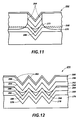
- the quantum wire semiconductor laser structure 262 including an optical waveguide 264 and a buried quantum wire 266 is identical in structure to the quantum wire semiconductor laser structure 216 of Figure 9 except that the disordering impurity source layer 268 of Figure 11 is epitaxially deposited between the first outer cladding layer 270 of n-Al x Ga 1-x As and the first inner confinement layer 272 of n-Al y Ga 1-y As where x>y.
- the impurity source layer 268 could comprise n-GaAs heavily doped, for example, with Zn up to a point of saturated concentration of the Zn elemental constituent in GaAs. Zn moves faster than Si and so would therefore be likely to disorder the subsequently epitaxially deposited semiconductor layers during the growth of those remaining layers.
- Impurity induced disordering has the additional benefit of eliminating most, if not all, of the quantum well layer remaining on top of the mesas after the desorption.
- the addition of the layer disordering regions also provides a measure of current confinement.
- Figure 12 discloses a semiconductor laser structure with a series of linear or horizontal multiple quantum wires.
- the horizontal multiple quantum wire semiconductor laser structure 274 includes a single substrate 276 of n-GaAs, upon which multiple V-shaped grooves 278 have been fabricated in series.
- the desorbing laser beam can either be a single laser beam or combination beam working in sequence, or more appropriately, multiple laser beams or combination laser beams working in parallel.
- a thinned quantum well layer 290 remains on the mesas of the inner confinement layer 284 and thence the sequential growth of a second inner confinement layer 292 of p-Al y Ga 1-y As forming multiple grooves 294 aligned with the grooves 286, 282 and 278; second outer cladding layer 296 of p-Al A Ga 1-A As where x ⁇ or ⁇ A>y forming multiple grooves 298 aligned with grooves 294, 286, 282 and 278; and cap layer 300 of p+-GaAs forming multiple grooves 302 aligned with grooves 298, 294, 286, 282 and 278.
- Multiple active quantum wires provide more modal gain for the laser cavity as compared to single quantum wire active regions.
- Standard chemical etching means or other metallization techniques are employed to form a p-contact on the cap layer 300 and a n-contact on the substrate 276 (not shown).
- the p-cladding layer 296 and the n-cladding layer 280 form a p-n junction with the quantum wires 288 therebetween.
- Current is injected between the p-contact and the n-contact to forward-bias the p-n junction of p-cladding layer 296 and the n-cladding layer 280 to cause the active quantum wires 288 to emit coherent radiation.
- Figure 13 discloses an alternative embodiment of a semiconductor laser structure with a series of linear or horizontal multiple quantum wires wherein the output is perpendicular to the axis of the multiple quantum wires.
- the horizontal multiple quantum wire semiconductor laser structure 304 includes a single substrate 306 of n-GaAs with grooves (not shown). The grooves in this and subsequent layers are not shown in this perspective of this Figure but are aligned as described with regard to the multiple quantum wire semiconductor laser of Figure 12.
- the desorbing laser beam can either be a single laser beam or combination beam working in sequence, or more appropriately, multiple laser beams or combination laser beams working in parallel.
- a thinned quantum well layer (not shown) remains on the mesas (also not shown) of the first inner confinement layer 310 and thence the sequential growth of a second inner confinement layer 314 of p-Al y Ga 1-y As forming multiple grooves (not shown) and an impurity source layer 316 comprising heavily doped n-GaAs.
- Impurity source layer 316 is shown in thick broken lines in Figure 13 to emphasize its higher dopant property.
- the impurity source is either deposited on the second inner confinement layer 314 in linear stripes perpendicular to the quantum wires, leaving a linear stripe section in the source layer free of the impurity source to form an array of quantum wire lasers, or the impurity source is deposited over the entire second inner layer and a linear stripe in the source layer is desorbed over a section of the quantum wires to form a single laser, perpendicular to the quantum wires.
- the epitaxial growth continues with the deposition of the second outer cladding layer 318 of p-Al A Ga 1-A As where x ⁇ A>y forming multiple grooves (not shown) and cap layer 320 of p+-GaAs forming multiple grooves (also not shown).
- annealing of the impurity disordering source 316 during the epitaxial growth of the last two semiconductor layers 318 and 320 causes impurity induced diffusion of impurity species from source layer 316 with the interdiffusion of Ga and Al and the formation of disordered regions 322 as illustrated in Figure 13 from the second outer cladding layer 318 through the other semiconductor layers to the first outer cladding layer 308.
- the impurity disordering source layer can be deposited on the cap layer, or on the second outer cladding layer, or between the first cladding and first confinement layers to produce the disordered regions.
- the multiple quantum wire semiconductor laser structure 304 includes a linear or horizontal series of quantum wires 312 for lightwave generation and propagation under lasing conditions bounded between by impurity disordered regions 322.
- Lightwave generation and propagation is perpendicular to the disordered region bounded quantum wires.
- the uniform active layer of the previous embodiments running the lengths of the quantum wire is replaced by an active layer covering only the widths of the quantum wires 312 with the inner confinement layers 310 and 314 between the quantum wires.
- the optical gain is localized to the quantum wires.
- the optical cavity 326 of the laser has a corrugated active layer from front laser mirror 328 to rear laser mirror 330. This orientation may provide the highest gain for a multiple quantum wire semiconductor laser structure since the radiative transition rate is largest for an optical field polarized along the quantum wire, i.e. corresponding to the preferred mode (TE) of the optical cavity.
- Standard chemical etching means or other metallization techniques are employed to form a p-contact on the cap layer 320 and a n-contact on the substrate 310 (not shown).
- the p-cladding layer 318 and the n-cladding layer 308 form a p-n junction with the quantum wires 312 therebetween.
- Current is injected between the p-contact and the n-contact to forward-bias the p-n junction of p-cladding layer 318 and the n-cladding layer 308 to cause the optical cavity 326 to emit coherent radiation.
- the quantum wires can also be spaced at n ⁇ /2 to form a distributed feedback (DFB) structure and thereby eliminate the necessity for cleaved laser end mirrors.
- DFB distributed feedback
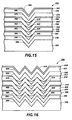
- Figure 15 discloses a semiconductor laser 332 with a series of sequential grown vertical quantum wells above a single groove in the substrate.
- the vertical multiple quantum wire semiconductor laser structure 332 includes a single substrate 334 of n-GaAs, upon which a single groove 336 has been fabricated.
- a thinned quantum well layer 348 remains on top of the inner confinement layer 342.
- Another quantum well layer is grown on top of the barrier layer 350 and photo induced desorbed leaving a quantum wire 354 at the vertex of the groove 352 and a thinned quantum well layer 356 on top of the barrier layer 308.
- Another barrier layer 358 is deposited forming a groove 360 aligned with the previous grooves, followed by a quantum well layer being deposited, which is desorbed to leave a quantum wire 362 at the vertex of the groove 360, and a thinned quantum well layer 364 on top of the barrier layer 358.
- Another barrier layer 366 is deposited forming a groove 368 aligned with the previous grooves, followed by a quantum well layer being deposited, which is desorbed to leave a quantum wire 370 at the vertex of the groove 368, and a thinned quantum well layer 372 on top of the barrier layer 366.
- Epitaxial growth is then continued with the growth of a second inner confinement layer 374 of p-Al y Ga 1-y As forming a groove 376 aligned with the previous grooves and second outer cladding layer 378 of p-Al A Ga 1-A As where x ⁇ or ⁇ A ⁇ y forming a groove 380 aligned with the previous grooves and cap layer 382 of p+-GaAs forming a groove 384 aligned with the previous grooves.
- Standard chemical etching means or other metallization techniques are employed to form a p-contact on the cap layer 382 and a n-contact on the substrate 334 (not shown).
- the p-cladding layer 378 and the n-cladding layer 338 form a p-n junction with the quantum wires 370, 362, 354, and 346 therebetween.
- Current is injected between the p-contact and the n-contact to forward-bias the p-n junction of p-cladding layer 378 and the n-cladding layer 338 to cause the active quantum wires 370, 362, 354, and 346 to emit coherent light.
- the barrier layers do not affect the p-n junction's ability to forward-bias the quantum wires and to emit light.
- Current confinement can be provided with a reverse bias layer, as taught previously, on the substrate or n-side, on the p-side, or on both sides of the quantum wires.
- Optical waveguides also as previously taught, can be provided for this embodiment.
- the barrier layer follows the contour of the previous cladding or barrier layer.
- an aligned groove will form in the barrier layer when the barrier layer is epitaxially deposited on top of the cladding layer.
- the sequentially grown quantum wires of Figure 15 are all self-aligned by the formation of the grooves.
- This growth sequence of alternating barrier layers and quantum well layers to be desorbed into quantum wires in the vertex of the grooves of the barrier layers can be repeated to form as many quantum wires as desired.
- Multiple active quantum wires provide more modal gain for the laser cavity as compared to single quantum wire active regions.
- a two-dimensional array multiple quantum wire semiconductor laser structure 386 is formed by sequentially growing more than one quantum wire on each of the series of multiple grooves fabricated in the substrate.
- Multiple quantum wire semiconductor laser structure 386 includes a substrate 388 of n-GaAs upon which is fabricated a series of grooves 390.
- a thinned quantum well layer 402 remains on the mesas of the inner confinement layer 396.
- Another quantum well layer is grown on top of the barrier layer 404 and photo induced desorbed leaving quantum wires 408 at the vertexes of the grooves 398 and a thinned quantum well layer 410 on the mesas of the barrier layer 404.
- the barrier layers and horizontal series of quantum wires can be repeated as many times as desired in vertical layers.
- series of quantum wires 414 in grooves 416 and barrier layer 418 is epitaxially deposited a second inner confinement layer 420 of p-Al y Ga 1-y As forming grooves 422 and second outer cladding layer 424 of p-Al A Ga 1-A As where x ⁇ or ⁇ A ⁇ y forming grooves 426 and cap layer 428 of p+-GaAs forming grooves 3430.
- Two-dimensional arrays of active quantum wires provide increased modal gain for the laser cavity as compared to active regions containing a single quantum wire or a one-dimensional array of quantum wires, either horizontally or vertically.
- the processing techniques permit the full in situ processing of a quantum wire without removal of the semiconductor structure from the MOCVD reactor or movement or masking of the structure in the reactor.
- the series of multiple grooves for the horizontal and two-dimensional array multiple quantum wire semiconductor laser structures can be fabricated in the outer cladding layer, rather than the substrate.
- the vertical and two-dimensional array multiple quantum wire semiconductor laser structures can be fabricated wherein the light output is perpendicular to the axis of the multiple quantum wires.
- Reverse bias junctions and optical waveguides can be fabricated with the various embodiments of the quantum wire semiconductor laser structures.
- Group III-V alloys may be employed in the practice of this invention, such as InGaP, InGaAsP, GaAlAsP, InGaAlP, InGaAlAsP, InP or GaAlSb or Group II-VI materials, e.g., ZnSe, ZnSSe and CdS.
- Group IV materials most importantly Si and Ge, may be utilized as semiconductor layers or a multiple quantum well structure of alternating well layers of GaAs or Al z Ga 1-z As and corresponding barrier layers of either AlAs or Al z Ga 1-z As where x>y>z′>z.
- different quantum wires can be of different quantum well semiconductor material depending upon circumstances and needs.
- the active layer may, in the alternative, be nondoped or p-type doped or n-type doped; GaAs, Al y Ga 1-y As or (Al x Ga 1-x ) 0.5 ln 0.5 P; or a relatively thin conventional double heterostructure (DH) active layer; or a single quantum well, such as GaAs or Al y Ga 1-y As where y ⁇ x; or a multiple quantum well superlattice, such as alternating layers of GaAs and Al y Ga 1-y As where y ⁇ x or alternating layers of Al w Ga 1-w As and Al B Ga 1-B As where B ⁇ w ⁇ x with a second cladding layer of p-Al z Ga 1-z As where B ⁇ w ⁇ z; or a separate single or multiple quantum well structure in a separate confinement cavity.
- DH conventional double heterostructure
Landscapes
- Physics & Mathematics (AREA)
- Optics & Photonics (AREA)
- Condensed Matter Physics & Semiconductors (AREA)
- General Physics & Mathematics (AREA)
- Electromagnetism (AREA)
- Engineering & Computer Science (AREA)
- Chemical & Material Sciences (AREA)
- Nanotechnology (AREA)
- Life Sciences & Earth Sciences (AREA)
- Biophysics (AREA)
- Geometry (AREA)
- Crystallography & Structural Chemistry (AREA)
- Semiconductor Lasers (AREA)
Applications Claiming Priority (2)
| Application Number | Priority Date | Filing Date | Title |
|---|---|---|---|
| US07/638,589 US5138625A (en) | 1991-01-08 | 1991-01-08 | Quantum wire semiconductor laser |
| US638589 | 1991-01-08 |
Publications (3)
| Publication Number | Publication Date |
|---|---|
| EP0494766A2 true EP0494766A2 (fr) | 1992-07-15 |
| EP0494766A3 EP0494766A3 (en) | 1992-10-21 |
| EP0494766B1 EP0494766B1 (fr) | 1997-03-05 |
Family
ID=24560637
Family Applications (1)
| Application Number | Title | Priority Date | Filing Date |
|---|---|---|---|
| EP92300143A Expired - Lifetime EP0494766B1 (fr) | 1991-01-08 | 1992-01-08 | Lasers à semi-conducteurs |
Country Status (4)
| Country | Link |
|---|---|
| US (1) | US5138625A (fr) |
| EP (1) | EP0494766B1 (fr) |
| JP (1) | JPH04296083A (fr) |
| DE (1) | DE69217679T2 (fr) |
Cited By (2)
| Publication number | Priority date | Publication date | Assignee | Title |
|---|---|---|---|---|
| EP0709902A1 (fr) * | 1994-10-26 | 1996-05-01 | Mitsubishi Chemical Corporation | Dispositif semi-conducteur et procédé de fabrication |
| EP1037342A3 (fr) * | 1999-03-08 | 2001-12-05 | Matsushita Electric Industrial Co., Ltd. | Laser à semiconducteur et méthode de fabrication |
Families Citing this family (16)
| Publication number | Priority date | Publication date | Assignee | Title |
|---|---|---|---|---|
| US5319661A (en) * | 1990-12-27 | 1994-06-07 | The Furukawa Electric Co., Ltd. | Semiconductor double heterostructure laser device with InP current blocking layer |
| US5175740A (en) * | 1991-07-24 | 1992-12-29 | Gte Laboratories Incorporated | Semiconductor laser and method of fabricating same |
| US6320200B1 (en) | 1992-06-01 | 2001-11-20 | Yale University | Sub-nanoscale electronic devices and processes |
| US5475341A (en) * | 1992-06-01 | 1995-12-12 | Yale University | Sub-nanoscale electronic systems and devices |
| US5311533A (en) * | 1992-10-23 | 1994-05-10 | Polaroid Corporation | Index-guided laser array with select current paths defined by migration-enhanced dopant incorporation and dopant diffusion |
| JP2767676B2 (ja) * | 1993-03-19 | 1998-06-18 | 松下電器産業株式会社 | 化合物半導体の微細構造形成方法 |
| US5689603A (en) * | 1993-07-07 | 1997-11-18 | Huth; Gerald C. | Optically interactive nanostructure |
| JPH0738194A (ja) * | 1993-07-20 | 1995-02-07 | Mitsubishi Electric Corp | 半導体レーザ及びその製造方法 |
| US5546418A (en) * | 1993-07-28 | 1996-08-13 | Matsushita Electric Industrial Co., Ltd. | Semiconductor laser having a flat groove for selected crystal planes |
| JPH08172217A (ja) * | 1994-12-19 | 1996-07-02 | Fujitsu Ltd | 光半導体装置 |
| KR0185498B1 (ko) * | 1996-05-22 | 1999-03-20 | 박원훈 | 고출력 양자세선 어레이 레이저 다이오드 구조 제작방법 |
| US5793913A (en) * | 1996-07-10 | 1998-08-11 | Northern Telecom Limited | Method for the hybrid integration of discrete elements on a semiconductor substrate |
| KR19990024760A (ko) | 1997-09-08 | 1999-04-06 | 정선종 | 양자세선 제조 방법 |
| US6803603B1 (en) * | 1999-06-23 | 2004-10-12 | Kabushiki Kaisha Toshiba | Semiconductor light-emitting element |
| US6574256B1 (en) | 2000-01-18 | 2003-06-03 | Xerox Corporation | Distributed feedback laser fabricated by lateral overgrowth of an active region |
| US6594295B1 (en) * | 2001-11-16 | 2003-07-15 | Fox-Tek, Inc. | Semiconductor laser with disordered and non-disordered quantum well regions |
Family Cites Families (16)
| Publication number | Priority date | Publication date | Assignee | Title |
|---|---|---|---|---|
| JPS5925399B2 (ja) * | 1979-11-28 | 1984-06-16 | 三菱電機株式会社 | 半導体レ−ザの製造方法 |
| JPS5723292A (en) * | 1980-07-16 | 1982-02-06 | Sony Corp | Semiconductor laser device and manufacture thereof |
| JPS57162484A (en) * | 1981-03-31 | 1982-10-06 | Fujitsu Ltd | Semiconductor luminous device |
| US4504952A (en) * | 1982-06-01 | 1985-03-12 | At&T Bell Laboratories | Stripe-guide TJS laser |
| JPS58220485A (ja) * | 1982-06-17 | 1983-12-22 | Fujitsu Ltd | 半導体発光装置及びその製造方法 |
| JPS6180881A (ja) * | 1984-09-28 | 1986-04-24 | Toshiba Corp | 半導体レ−ザ装置 |
| JPS61102086A (ja) * | 1984-10-24 | 1986-05-20 | Mitsubishi Electric Corp | 半導体レ−ザ |
| GB8518353D0 (en) * | 1985-07-20 | 1985-08-29 | Plessey Co Plc | Heterostructure device |
| US4839307A (en) * | 1986-05-14 | 1989-06-13 | Omron Tateisi Electronics Co. | Method of manufacturing a stripe-shaped heterojunction laser with unique current confinement |
| US4860298A (en) * | 1988-04-12 | 1989-08-22 | Dan Botez | Phased-locked array of semiconductor lasers using closely spaced antiguides |
| GB8806800D0 (en) * | 1988-03-22 | 1988-04-20 | British Telecomm | Etching methods |
| US4874690A (en) * | 1988-08-26 | 1989-10-17 | Cryopharm Corporation | Lyophilization of red blood cells |
| US4962057A (en) * | 1988-10-13 | 1990-10-09 | Xerox Corporation | Method of in situ photo induced evaporation enhancement of compound thin films during or after epitaxial growth |
| US5013684A (en) * | 1989-03-24 | 1991-05-07 | Xerox Corporation | Buried disordering sources in semiconductor structures employing photo induced evaporation enhancement during in situ epitaxial growth |
| US4980314A (en) * | 1989-06-06 | 1990-12-25 | At&T Bell Laboratories | Vapor processing of a substrate |
| JP2854607B2 (ja) * | 1989-06-29 | 1999-02-03 | 株式会社日立製作所 | 半導体装置及び半導体レーザ装置 |
-
1991
- 1991-01-08 US US07/638,589 patent/US5138625A/en not_active Expired - Lifetime
- 1991-12-27 JP JP3347011A patent/JPH04296083A/ja active Pending
-
1992
- 1992-01-08 DE DE69217679T patent/DE69217679T2/de not_active Expired - Lifetime
- 1992-01-08 EP EP92300143A patent/EP0494766B1/fr not_active Expired - Lifetime
Cited By (6)
| Publication number | Priority date | Publication date | Assignee | Title |
|---|---|---|---|---|
| EP0709902A1 (fr) * | 1994-10-26 | 1996-05-01 | Mitsubishi Chemical Corporation | Dispositif semi-conducteur et procédé de fabrication |
| US6589807B2 (en) | 1994-10-26 | 2003-07-08 | Mitsubishi Chemical Corporation | Semiconductor device and method for manufacturing the same |
| US6744066B2 (en) | 1994-10-26 | 2004-06-01 | Mitsubishi Chemical Corporation | Semiconductor device and method for manufacturing the same |
| EP1037342A3 (fr) * | 1999-03-08 | 2001-12-05 | Matsushita Electric Industrial Co., Ltd. | Laser à semiconducteur et méthode de fabrication |
| US6625189B1 (en) | 1999-03-08 | 2003-09-23 | Matsushita Electric Industrial Co., Ltd. | Semiconductor laser device and fabrication method thereof |
| US6933159B2 (en) | 1999-03-08 | 2005-08-23 | Matsushita Electric Industrial Co., Ltd. | Fabrication method of a semiconductor laser device |
Also Published As
| Publication number | Publication date |
|---|---|
| US5138625A (en) | 1992-08-11 |
| EP0494766A3 (en) | 1992-10-21 |
| JPH04296083A (ja) | 1992-10-20 |
| DE69217679D1 (de) | 1997-04-10 |
| EP0494766B1 (fr) | 1997-03-05 |
| DE69217679T2 (de) | 1997-07-31 |
Similar Documents
| Publication | Publication Date | Title |
|---|---|---|
| EP0494765B1 (fr) | Lasers à semi-conducteur | |
| EP0494766B1 (fr) | Lasers à semi-conducteurs | |
| US6600169B2 (en) | Quantum dash device | |
| US5048038A (en) | Ion-implanted planar-buried-heterostructure diode laser | |
| EP0661782A1 (fr) | Laser à semi-conducteur | |
| JP2545188B2 (ja) | 埋込みヘテロ構造レ―ザ | |
| US5013684A (en) | Buried disordering sources in semiconductor structures employing photo induced evaporation enhancement during in situ epitaxial growth | |
| EP0503211B1 (fr) | Dispositif semi-conducteur comprenant une structure en couches fabriquée par croissance sur un substrat structuré | |
| US5436191A (en) | Quantum wire fabrication via photo induced evaporation enhancement during in situ epitaxial growth | |
| GB2280311A (en) | Semiconductor laser | |
| Hobson | Epitaxial Growth, Fabrication, and Performance of Ingaas Strained Quantum Well Laser Structures | |
| US5102825A (en) | Method of making an ion-implanted planar-buried-heterostructure diode laser | |
| JP4002422B2 (ja) | 半導体素子およびその作製方法 | |
| EP0293000B1 (fr) | Dispositif émetteur de lumière | |
| Tanaka et al. | MBE as a production technology for AlGaAs lasers | |
| WO1997036335A1 (fr) | Diode a semi-conducteur emettrice de rayonnement ayant une couche de confinement separee comprenant un materiau semi-conducteur avec 30 % d'aluminium au maximum, ou un materiau semi-conducteur exempt d'aluminium | |
| US5563094A (en) | Buried reverse bias junction configurations in semiconductor structures employing photo induced evaporation enhancement during in situ epitaxial growth and device structures utilizing the same | |
| Tappura et al. | High-power GaInP-AlGaInP quantum-well lasers grown by solid source molecular beam epitaxy | |
| JP2001185809A (ja) | 半導体光デバイス装置及びその製造方法 | |
| JP2001203423A (ja) | 半導体発光装置 | |
| JP3665911B2 (ja) | 半導体光素子の製造方法,及び半導体光素子 | |
| Gailhanou et al. | Chemical beam epitaxial selective growth of InP for laser fabrication | |
| Yoshikawa et al. | A novel technology for formation of a narrow active layer in buried heterostructure lasers by single-step MOCVD | |
| CA1282874C (fr) | Dispositifs a semiconducteur a couche epitaxiale a grande resistivite pour confiner le courant | |
| Toivonen et al. | High-performance GaInP/AlGaInP strained quantum well lasers grown by solid source molecular beam epitaxy |
Legal Events
| Date | Code | Title | Description |
|---|---|---|---|
| PUAI | Public reference made under article 153(3) epc to a published international application that has entered the european phase |
Free format text: ORIGINAL CODE: 0009012 |
|
| AK | Designated contracting states |
Kind code of ref document: A2 Designated state(s): DE FR GB |
|
| PUAL | Search report despatched |
Free format text: ORIGINAL CODE: 0009013 |
|
| AK | Designated contracting states |
Kind code of ref document: A3 Designated state(s): DE FR GB |
|
| 17P | Request for examination filed |
Effective date: 19930401 |
|
| 17Q | First examination report despatched |
Effective date: 19931018 |
|
| GRAG | Despatch of communication of intention to grant |
Free format text: ORIGINAL CODE: EPIDOS AGRA |
|
| GRAH | Despatch of communication of intention to grant a patent |
Free format text: ORIGINAL CODE: EPIDOS IGRA |
|
| GRAH | Despatch of communication of intention to grant a patent |
Free format text: ORIGINAL CODE: EPIDOS IGRA |
|
| GRAA | (expected) grant |
Free format text: ORIGINAL CODE: 0009210 |
|
| AK | Designated contracting states |
Kind code of ref document: B1 Designated state(s): DE FR GB |
|
| REF | Corresponds to: |
Ref document number: 69217679 Country of ref document: DE Date of ref document: 19970410 |
|
| ET | Fr: translation filed | ||
| PLBE | No opposition filed within time limit |
Free format text: ORIGINAL CODE: 0009261 |
|
| 26N | No opposition filed | ||
| REG | Reference to a national code |
Ref country code: GB Ref legal event code: IF02 |
|
| PGFP | Annual fee paid to national office [announced via postgrant information from national office to epo] |
Ref country code: FR Payment date: 20110128 Year of fee payment: 20 Ref country code: DE Payment date: 20110105 Year of fee payment: 20 |
|
| PGFP | Annual fee paid to national office [announced via postgrant information from national office to epo] |
Ref country code: GB Payment date: 20110105 Year of fee payment: 20 |
|
| REG | Reference to a national code |
Ref country code: DE Ref legal event code: R071 Ref document number: 69217679 Country of ref document: DE |
|
| REG | Reference to a national code |
Ref country code: DE Ref legal event code: R071 Ref document number: 69217679 Country of ref document: DE |
|
| REG | Reference to a national code |
Ref country code: GB Ref legal event code: PE20 Expiry date: 20120107 |
|
| PG25 | Lapsed in a contracting state [announced via postgrant information from national office to epo] |
Ref country code: DE Free format text: LAPSE BECAUSE OF EXPIRATION OF PROTECTION Effective date: 20120109 |
|
| PG25 | Lapsed in a contracting state [announced via postgrant information from national office to epo] |
Ref country code: GB Free format text: LAPSE BECAUSE OF EXPIRATION OF PROTECTION Effective date: 20120107 |