EP0495400A2 - Câble optique et procédé de sa fabrication - Google Patents
Câble optique et procédé de sa fabrication Download PDFInfo
- Publication number
- EP0495400A2 EP0495400A2 EP92100295A EP92100295A EP0495400A2 EP 0495400 A2 EP0495400 A2 EP 0495400A2 EP 92100295 A EP92100295 A EP 92100295A EP 92100295 A EP92100295 A EP 92100295A EP 0495400 A2 EP0495400 A2 EP 0495400A2
- Authority
- EP
- European Patent Office
- Prior art keywords
- chambers
- optical cable
- elements
- cable according
- core element
- Prior art date
- Legal status (The legal status is an assumption and is not a legal conclusion. Google has not performed a legal analysis and makes no representation as to the accuracy of the status listed.)
- Granted
Links
- 230000003287 optical effect Effects 0.000 title claims abstract description 30
- 238000000034 method Methods 0.000 title claims description 11
- 238000004519 manufacturing process Methods 0.000 title claims description 8
- 239000013307 optical fiber Substances 0.000 claims description 6
- 238000005192 partition Methods 0.000 claims description 4
- 230000008569 process Effects 0.000 claims description 4
- 150000001875 compounds Chemical class 0.000 claims description 2
- 238000003780 insertion Methods 0.000 claims description 2
- 230000037431 insertion Effects 0.000 claims description 2
- 238000013461 design Methods 0.000 description 4
- 108010020053 Staphylococcus warneri lipase 2 Proteins 0.000 description 2
- 230000008901 benefit Effects 0.000 description 2
- 238000010276 construction Methods 0.000 description 2
- 238000011161 development Methods 0.000 description 2
- 230000018109 developmental process Effects 0.000 description 2
- 238000001125 extrusion Methods 0.000 description 2
- 238000009987 spinning Methods 0.000 description 2
- 239000004698 Polyethylene Substances 0.000 description 1
- 229910000831 Steel Inorganic materials 0.000 description 1
- 230000008859 change Effects 0.000 description 1
- 239000000835 fiber Substances 0.000 description 1
- 239000011152 fibreglass Substances 0.000 description 1
- 239000000463 material Substances 0.000 description 1
- 238000012856 packing Methods 0.000 description 1
- 239000006223 plastic coating Substances 0.000 description 1
- -1 polyethylene Polymers 0.000 description 1
- 229920000573 polyethylene Polymers 0.000 description 1
- 230000007480 spreading Effects 0.000 description 1
- 238000003892 spreading Methods 0.000 description 1
- 239000010959 steel Substances 0.000 description 1
- 230000007704 transition Effects 0.000 description 1
- 238000004804 winding Methods 0.000 description 1
Images


Classifications
-
- G—PHYSICS
- G02—OPTICS
- G02B—OPTICAL ELEMENTS, SYSTEMS OR APPARATUS
- G02B6/00—Light guides; Structural details of arrangements comprising light guides and other optical elements, e.g. couplings
- G02B6/44—Mechanical structures for providing tensile strength and external protection for fibres, e.g. optical transmission cables
- G02B6/4401—Optical cables
- G02B6/4403—Optical cables with ribbon structure
-
- G—PHYSICS
- G02—OPTICS
- G02B—OPTICAL ELEMENTS, SYSTEMS OR APPARATUS
- G02B6/00—Light guides; Structural details of arrangements comprising light guides and other optical elements, e.g. couplings
- G02B6/44—Mechanical structures for providing tensile strength and external protection for fibres, e.g. optical transmission cables
- G02B6/4401—Optical cables
- G02B6/4407—Optical cables with internal fluted support member
- G02B6/4408—Groove structures in support members to decrease or harmonise transmission losses in ribbon cables
-
- G—PHYSICS
- G02—OPTICS
- G02B—OPTICAL ELEMENTS, SYSTEMS OR APPARATUS
- G02B6/00—Light guides; Structural details of arrangements comprising light guides and other optical elements, e.g. couplings
- G02B6/44—Mechanical structures for providing tensile strength and external protection for fibres, e.g. optical transmission cables
- G02B6/4479—Manufacturing methods of optical cables
- G02B6/449—Twisting
- G02B6/4491—Twisting in a lobe structure
Definitions
- the invention relates to an optical cable with chambers distributed over the circumference, which are used to hold stacks of ribbons, each of which is composed of a number of ribbons comprising a plurality of optical waveguides, the chamber walls being separated by partition walls.
- each ribbon stack contains several optical waveguide ribbons, and the chamber itself is designed with a rectangular cross section and is open to the outside.
- the invention has for its object to provide an optical cable that can be manufactured in a simple manner and in which a large number of optical fibers can be accommodated in the region of the cable core. According to the invention, this object is achieved with an optical cable of the type mentioned in that chambers are provided which open inwards, that each chamber has a cross section approximately U-shaped, outwardly widening partial element is formed and that several such partial elements are arranged in segments around a core element.
- the inwardly open chambers are thus seated on the core element, so that a stable, well-bearing construction results. It also ensures that the walls between the individual abutting sub-elements can be designed so that a space-saving construction is achieved.
- the invention in the area of the base, i.e. where the chamber walls meet the core element, no minimum wall thickness is required. If, on the other hand, chambers that are open to the outside are produced by extrusion of an approximately spoke wheel-shaped chamber element onto a tensile core, then a minimum thickness is also required for the chamber wall in the region of the chamber base, which for stability and manufacturing reasons cannot be undercut.
- the invention further relates to a method for producing an optical cable, which is characterized in that the partial elements containing the chambers or the central element or the core element are provided with the ribbon stacks, that the partial elements together with the ribbon stacks contained therein or on the core element be applied in multiple layers and that at least one outer jacket is then applied.
- a core element EG is provided, which can suitably consist of a tensile material (steel or glass fiber reinforced plastic, for example).
- a plastic coating CL can be provided here.
- a total of six chamber elements (sub-elements), CE1-CE6 are arranged on this core element EC in a segment-shaped arrangement in such a way that their respective chambers CA1-CA6 point with the opening inwards, ie in the direction of the core element EC.
- the chambers CA1-CA6 have an approximately rectangular cross section and in each of these chambers a ribbon stack BS1-BS6 is accommodated, which consists of several ribbons.
- each of these tapes BD1-BD5 contains a number of optical waveguides, in the present example, as shown in the tape BD1, six optical waveguides LW1-LW2 are introduced into a common envelope forming the ribbon.
- the introduction of the stack of tapes BS1-BS6 into the chambers CA1-CA6 is expediently carried out in such a way that it continues to maintain a certain degree of mobility, while avoiding a change of position (folding over or tipping over). It is sufficient if a narrow gap is provided all around the ribbon stack.
- the straps BD1-BD5 can be rotatable / foldable within the chamber CA1, it also being advantageous to twist the straps with changing directions (in the manner of SZ stranding).
- the partial elements CE1-CE6, each with a U-shaped cross-section, are designed for their side legs (SWL and SWR for CE1) so that they taper inwards.
- the wall thickness is reduced to values between 0 mm (i.e. design as a tip) and 0.5 mm. These values are much smaller than e.g. in such arrangements in which radially outwardly opening chambers are provided because cross-sectional transitions need not be taken into account. There it is namely not possible to reduce the wall thickness in the area of the core element CE to such small values for manufacturing and strength considerations.
- the cohesion of the partial elements CE1-CE6 stranded on the core element EC can e.g. be ensured by wrapping or spinning BF.
- a (possibly multi-layered) outer jacket MA is applied further out, e.g. by extruding.
- the optical cable OC thus obtained is characterized by a compact structure, offers the possibility of accommodating a large number of optical waveguides for a given cross section and enables simple and efficient production.
- the chamber for example of the partial element CE21
- the chamber is no longer formed with an approximately rectangular cross section, but is also designed in the form of a segment.
- an outwardly widening chamber is created and there is the possibility of providing ribbon stacks BD21-BD25 which fill up as far as possible the space of the chamber CA21 that is spreading outwards.
- the ribbons become wider from the inside to the outside and can therefore each contain a larger number of optical fibers.
- the packing density of the optical waveguides can thus be increased considerably for a given cable cross section or cross section of the cable core.
- the wall thickness of the side walls SWL2 and SWR2 of the partial element CE21 is expediently chosen so that it remains the same from the inside to the outside. Wall thicknesses in the range between 0.5 mm and 1 mm are sufficient for the side walls SWL2 and SWR2. It is assumed that the entire part element CE21 is produced by extrusion, for example from polyethylene.
- a larger number of fibers can be used multilayer design may be appropriate, as shown in Fig. 3.
- an inner layer (similar to FIG. 1) of six segment-shaped partial elements CEI1-CEI6 is initially provided on the core element EC3, the outer structure of which corresponds to the arrangement according to FIG. 1. It may be useful to e.g. Before the next layer of segment-shaped sub-elements is applied, provision should be made for winding or spinning in order to secure the position of the inner elements CEI1-CEI6.
- a second layer of segment-shaped partial elements CEA1-CEA12 the arrangement advantageously being such that webs or partitions of the inner partial elements CEI1-CEI6 and the outer partial elements CEA1-CEA12 seen in the radial direction are not aligned with each other.
- the second layer of partial elements CEA1-CEA12 has approximately the same radial extent as the inner layer and also the extent of the partial elements CEA1-CEA12 approximately in the circumferential direction is similar to that of the inner layer.
- the inner layer (CI1-CI6) and the outer layer (CA1-CA12) are applied in opposite directions, ie in counter-lay, then the radial webs of the two layers cross each other continuously and a stable overall structure with high flexibility is created.
- One or both layers can also be roped in an SZ shape.
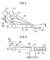
- FIG. 4 shows the process sequence for the production of an optical cable corresponding to FIG. 1.
- the sub-elements CE1, CE2, etc. have been prefabricated and are available wound on supply drums VC1 or VC2 etc.
- the tapes BD1-BD5 run from supply spools VB11-VB15, while supply spools VB21-VB25 are provided for the tapes of the stack BS2 of the sub-element CE2.
- All of the supply spools shown are arranged in a fixed manner, it being assumed that the tensile central element EC rotates about its longitudinal axis and is simultaneously pulled from left to right. However, it is also possible to design the core element EC to be stationary and to accommodate the supply spools in a rotating cage.
- the individual supply spools VB11-VB15 for the tapes BD1-BD5 are arranged in such a way that the tapes BD1-BD5, which are pulled off under a slight tensile stress, are already combined to form a stack BS1 shortly before the partial element CE1 strikes, and possibly come into contact with the core element EC.
- the partial elements CE1-CE6 can be applied using the same-lay method; but it is also possible to work with changing direction of stranding (SZ stranding), i.e. to subject the core element EC to a reverse rotation in certain successive time segments.
- SZ stranding changing direction of stranding
- the core element EC rotates, whereby, in contrast to the arrangement according to FIG. 4, the partial elements CE1-CE6 are not prefabricated, but are also only produced when the ribbon stack is applied.
- the tapes BD1-BD5, which form the tapes stack BS1 are likewise arranged on supply spools VB11-VB15 and are drawn off from them.
- the ribbon stack BS1 is created immediately before it enters the extruder head EK of an extruder EX.
- the outlets of the extruder head EK are designed so that, according to the example of FIG. 1, six independent partial elements CE1-CE6 are formed, each of which is practically extruded in the form of a bridge via the associated ribbon stack BS1-BS6 according to FIG. 1, a connection to the Core element EC is not required.
- a particular advantage of the cable structure according to the invention can also be seen in the fact that the sub-elements, for example CE1-CE5 according to FIG. 1, join together to form a closed annular structure on the outside, which overall (with regard to the load-bearing function) similar to a continuous pipe.
- the individual sub-elements thus form quasi-supporting vaults and thus - even with very small wall thicknesses of the partition walls - provide a stable overall structure due to the mutual lateral support.
- An approximately necessary excess length of the ribbon stacks BS1-BS6 according to FIG. 1 can be achieved by pushing them in when they are being applied to the core element EC.
- the associated shrinkage of the central element EC causes the relative excess length of the ribbon stack.
- the device according to FIG. 5 it is also possible to use the device according to FIG. 5 to extrude a closed central body ZK according to FIG. 6, the shape of which corresponds approximately to that of an internal toothing, i.e. the chambers CA51-CA5n are open inwards to the central element EC5.
- the one-piece central body ZK has been used.
- assemble the central body ZK from a plurality of partial central bodies, each of which comprises a plurality of chambers. This is indicated in FIG. 6 by dash-dotted radial dividing lines which form the partial central elements ZK1, ZK2 and ZK3.
Landscapes
- Physics & Mathematics (AREA)
- General Physics & Mathematics (AREA)
- Optics & Photonics (AREA)
- Engineering & Computer Science (AREA)
- Manufacturing & Machinery (AREA)
- Superconductors And Manufacturing Methods Therefor (AREA)
- Ropes Or Cables (AREA)
- Manufacturing Of Electric Cables (AREA)
- Light Guides In General And Applications Therefor (AREA)
- Extrusion Moulding Of Plastics Or The Like (AREA)
Applications Claiming Priority (2)
| Application Number | Priority Date | Filing Date | Title |
|---|---|---|---|
| DE4101271 | 1991-01-17 | ||
| DE4101271 | 1991-01-17 |
Publications (3)
| Publication Number | Publication Date |
|---|---|
| EP0495400A2 true EP0495400A2 (fr) | 1992-07-22 |
| EP0495400A3 EP0495400A3 (en) | 1993-01-13 |
| EP0495400B1 EP0495400B1 (fr) | 1996-12-18 |
Family
ID=6423205
Family Applications (1)
| Application Number | Title | Priority Date | Filing Date |
|---|---|---|---|
| EP92100295A Expired - Lifetime EP0495400B1 (fr) | 1991-01-17 | 1992-01-09 | Câble optique et procédé de sa fabrication |
Country Status (5)
| Country | Link |
|---|---|
| US (1) | US5210813A (fr) |
| EP (1) | EP0495400B1 (fr) |
| JP (1) | JP3073583B2 (fr) |
| AT (1) | ATE146605T1 (fr) |
| DE (1) | DE59207690D1 (fr) |
Cited By (8)
| Publication number | Priority date | Publication date | Assignee | Title |
|---|---|---|---|---|
| WO1993018423A1 (fr) * | 1992-03-03 | 1993-09-16 | Siemens Aktiengesellschaft | Cable optique et son procede de fabrication |
| WO1993018424A1 (fr) * | 1992-03-03 | 1993-09-16 | Siemens Aktiengesellschaft | Cable optique et son procede de fabrication |
| FR2706046A1 (fr) * | 1993-06-02 | 1994-12-09 | Siemens Ag | Câble optique, procédé pour sa fabrication et dispositif pour la mise en Óoeuvre du procédé. |
| FR2714977A1 (fr) * | 1994-01-12 | 1995-07-13 | Siemens Ag | Câble optique et son procédé de fabrication. |
| EP0694091A4 (fr) * | 1994-01-28 | 1996-05-08 | Ceeco Machinery Mfg | Procede et appareil d'enroulement de rubans plats autour de noyaux cylindriques |
| US5771321A (en) * | 1996-01-04 | 1998-06-23 | Massachusetts Institute Of Technology | Micromechanical optical switch and flat panel display |
| DE19910653A1 (de) * | 1999-03-10 | 2000-09-14 | Alcatel Sa | Metallfreies optisches Kabel |
| CN114675384A (zh) * | 2022-03-01 | 2022-06-28 | 富通集团有限公司 | 一种光缆 |
Families Citing this family (7)
| Publication number | Priority date | Publication date | Assignee | Title |
|---|---|---|---|---|
| US5420955A (en) * | 1994-06-22 | 1995-05-30 | Siecor Corporation | Optical cables having U-shaped carriers exhibiting enhanced crush performance |
| US5777260A (en) * | 1995-03-14 | 1998-07-07 | Siemens Aktiengesellschaft | Coaxial cable additionally having at least one light waveguide |
| US5649043A (en) * | 1995-07-25 | 1997-07-15 | Alcatel Na Cable Systems, Inc. | Optical fiber cable having truncated triangular profile tubes |
| US7156126B2 (en) * | 2001-11-14 | 2007-01-02 | Topek Philip R | Pipe insert and pipe assembly formed therewith |
| US7123801B2 (en) * | 2004-11-18 | 2006-10-17 | Prysmian Communications Cables And Systems Usa, Llc | Optical fiber cable with fiber receiving jacket ducts |
| US9605778B2 (en) * | 2013-08-02 | 2017-03-28 | Oceaneering International, Inc. | Extruded encapsulated fillers to provide crush protection |
| EP3346307A1 (fr) * | 2017-01-06 | 2018-07-11 | Sterlite Technologies Ltd | Tube làche pour câble à fibre optique |
Family Cites Families (7)
| Publication number | Priority date | Publication date | Assignee | Title |
|---|---|---|---|---|
| DE2449439C3 (de) * | 1974-10-15 | 1984-08-23 | Siemens AG, 1000 Berlin und 8000 München | Nachrichtenkabel mit Lichtleiter bzw. Lichtleiterbündel als Übertragungselemente |
| DE2928678B2 (de) * | 1979-07-16 | 1981-06-11 | Siemens AG, 1000 Berlin und 8000 München | Optisches Kabel |
| GB8531673D0 (en) * | 1985-12-23 | 1986-02-05 | Telephone Cables Ltd | Optical fibre units |
| JPH01163710A (ja) * | 1987-02-25 | 1989-06-28 | Sumitomo Electric Ind Ltd | 光ケ−ブル |
| DE3839109A1 (de) * | 1988-11-18 | 1990-05-23 | Siemens Ag | Optisches kabel mit mehreren kammerelementen |
| GB8908446D0 (en) * | 1989-04-14 | 1989-06-01 | Bicc Plc | Optical cable |
| JP3125308U (ja) | 2006-07-04 | 2006-09-14 | マルイチセーリング株式会社 | リクライニング・ソファ |
-
1991
- 1991-12-09 US US07/803,617 patent/US5210813A/en not_active Expired - Fee Related
-
1992
- 1992-01-09 AT AT92100295T patent/ATE146605T1/de not_active IP Right Cessation
- 1992-01-09 DE DE59207690T patent/DE59207690D1/de not_active Expired - Fee Related
- 1992-01-09 EP EP92100295A patent/EP0495400B1/fr not_active Expired - Lifetime
- 1992-01-13 JP JP04003742A patent/JP3073583B2/ja not_active Expired - Fee Related
Cited By (11)
| Publication number | Priority date | Publication date | Assignee | Title |
|---|---|---|---|---|
| WO1993018423A1 (fr) * | 1992-03-03 | 1993-09-16 | Siemens Aktiengesellschaft | Cable optique et son procede de fabrication |
| WO1993018424A1 (fr) * | 1992-03-03 | 1993-09-16 | Siemens Aktiengesellschaft | Cable optique et son procede de fabrication |
| US5487126A (en) * | 1992-03-03 | 1996-01-23 | Siemens Aktiengesellschaft | Optical cable and process for producing the same |
| US5542019A (en) * | 1992-03-03 | 1996-07-30 | Siemens Aktiengesellschaft | Optical cable and process for the manufacture thereof |
| FR2706046A1 (fr) * | 1993-06-02 | 1994-12-09 | Siemens Ag | Câble optique, procédé pour sa fabrication et dispositif pour la mise en Óoeuvre du procédé. |
| FR2714977A1 (fr) * | 1994-01-12 | 1995-07-13 | Siemens Ag | Câble optique et son procédé de fabrication. |
| EP0694091A4 (fr) * | 1994-01-28 | 1996-05-08 | Ceeco Machinery Mfg | Procede et appareil d'enroulement de rubans plats autour de noyaux cylindriques |
| US5771321A (en) * | 1996-01-04 | 1998-06-23 | Massachusetts Institute Of Technology | Micromechanical optical switch and flat panel display |
| DE19910653A1 (de) * | 1999-03-10 | 2000-09-14 | Alcatel Sa | Metallfreies optisches Kabel |
| CN114675384A (zh) * | 2022-03-01 | 2022-06-28 | 富通集团有限公司 | 一种光缆 |
| CN114675384B (zh) * | 2022-03-01 | 2023-05-09 | 富通集团有限公司 | 一种光缆 |
Also Published As
| Publication number | Publication date |
|---|---|
| ATE146605T1 (de) | 1997-01-15 |
| JP3073583B2 (ja) | 2000-08-07 |
| EP0495400B1 (fr) | 1996-12-18 |
| EP0495400A3 (en) | 1993-01-13 |
| DE59207690D1 (de) | 1997-01-30 |
| US5210813A (en) | 1993-05-11 |
| JPH04296805A (ja) | 1992-10-21 |
Similar Documents
| Publication | Publication Date | Title |
|---|---|---|
| EP0495400B1 (fr) | Câble optique et procédé de sa fabrication | |
| EP0492206B1 (fr) | Câble optique ayant guides d'onde lumineuses multiples | |
| DE3786877T2 (de) | Optisches Kabel. | |
| DE19734420B4 (de) | Verfahren und Vorrichtung zur Herstellung eines Kabels | |
| DE69506705T2 (de) | Faseroptisches kabel mit erweitertem kontraktionsbereich,verfahren und vorrichtung zur herstellung des kabels | |
| EP0429916B1 (fr) | Pièce de bourrage pour traversées de conducteurs | |
| DE4142047A1 (de) | Verfahren zum umhuellen mindestens eines lichtwellenleiters mit einer schutzschicht und zum anbringen von verstaerkungselementen | |
| EP0356786B1 (fr) | Câble optique avec un support central | |
| DE19841974A1 (de) | Borste für eine Zahnbürste, insbesondere für eine elektrische Zahnbürste, sowie Verfahren zu deren Herstellung | |
| DE3606617A1 (de) | Flachbandleitung mit mehreren lichtwellenleiteradern und verfahren zu deren herstellung | |
| EP0629298B1 (fr) | Cable optique et son procede de fabrication | |
| EP0629299B1 (fr) | Cable optique et son procede de fabrication | |
| DE69112876T2 (de) | Verbindung für optische Kabel und Kabelseele mit zugehörigem Herstellungsverfahren. | |
| DE3537553C2 (de) | Optisches Kabel mit mehreren Hauptbündeln | |
| DE3000674A1 (de) | Lichtleitfasern enthaltendes kabel und verfahren zu seiner herstellung | |
| DE19628457A1 (de) | Nachrichtenkabel, Verfahren sowie Vorrichtung zu dessen Herstellung | |
| DE19713063A1 (de) | Nachrichtenkabel | |
| EP0158730B1 (fr) | Dispositif avec deux accumulateurs tubulaires concentriques | |
| DE69601958T2 (de) | Vorrichtung zum Unterteilen einer Installationskabelröhre | |
| DE3526823A1 (de) | Element mit mehreren lichtwellenleitern | |
| EP0568962A1 (fr) | Dispositif pour la fabrication d'un produit vide pour la distribution des fibres optiques et procédé pour sa fabrication | |
| DE4040715A1 (de) | Optisches kabel mit einer vielzahl von lichtwellenleitern | |
| EP0498308B1 (fr) | Câble optique et procédé de sa fabrication | |
| DE69624787T2 (de) | Kabelhülle und verfahren zur herstellung | |
| DE4108569C2 (de) | Optisches Kabel und Verfahren zu seiner Herstellung |
Legal Events
| Date | Code | Title | Description |
|---|---|---|---|
| PUAI | Public reference made under article 153(3) epc to a published international application that has entered the european phase |
Free format text: ORIGINAL CODE: 0009012 |
|
| AK | Designated contracting states |
Kind code of ref document: A2 Designated state(s): AT BE CH DE FR GB IT LI NL SE |
|
| PUAL | Search report despatched |
Free format text: ORIGINAL CODE: 0009013 |
|
| AK | Designated contracting states |
Kind code of ref document: A3 Designated state(s): AT BE CH DE FR GB IT LI NL SE |
|
| 17P | Request for examination filed |
Effective date: 19930204 |
|
| 17Q | First examination report despatched |
Effective date: 19950901 |
|
| GRAG | Despatch of communication of intention to grant |
Free format text: ORIGINAL CODE: EPIDOS AGRA |
|
| GRAH | Despatch of communication of intention to grant a patent |
Free format text: ORIGINAL CODE: EPIDOS IGRA |
|
| GRAH | Despatch of communication of intention to grant a patent |
Free format text: ORIGINAL CODE: EPIDOS IGRA |
|
| GRAA | (expected) grant |
Free format text: ORIGINAL CODE: 0009210 |
|
| AK | Designated contracting states |
Kind code of ref document: B1 Designated state(s): AT BE CH DE FR GB IT LI NL SE |
|
| REF | Corresponds to: |
Ref document number: 146605 Country of ref document: AT Date of ref document: 19970115 Kind code of ref document: T |
|
| REG | Reference to a national code |
Ref country code: CH Ref legal event code: NV Representative=s name: SIEMENS SCHWEIZ AG |
|
| REF | Corresponds to: |
Ref document number: 59207690 Country of ref document: DE Date of ref document: 19970130 |
|
| ET | Fr: translation filed | ||
| ITF | It: translation for a ep patent filed | ||
| GBT | Gb: translation of ep patent filed (gb section 77(6)(a)/1977) |
Effective date: 19970220 |
|
| PLBE | No opposition filed within time limit |
Free format text: ORIGINAL CODE: 0009261 |
|
| STAA | Information on the status of an ep patent application or granted ep patent |
Free format text: STATUS: NO OPPOSITION FILED WITHIN TIME LIMIT |
|
| 26N | No opposition filed | ||
| PGFP | Annual fee paid to national office [announced via postgrant information from national office to epo] |
Ref country code: SE Payment date: 20001220 Year of fee payment: 10 Ref country code: GB Payment date: 20001220 Year of fee payment: 10 Ref country code: FR Payment date: 20001220 Year of fee payment: 10 Ref country code: DE Payment date: 20001220 Year of fee payment: 10 |
|
| PGFP | Annual fee paid to national office [announced via postgrant information from national office to epo] |
Ref country code: AT Payment date: 20001221 Year of fee payment: 10 |
|
| PGFP | Annual fee paid to national office [announced via postgrant information from national office to epo] |
Ref country code: CH Payment date: 20001222 Year of fee payment: 10 |
|
| PGFP | Annual fee paid to national office [announced via postgrant information from national office to epo] |
Ref country code: NL Payment date: 20001228 Year of fee payment: 10 |
|
| PGFP | Annual fee paid to national office [announced via postgrant information from national office to epo] |
Ref country code: BE Payment date: 20010123 Year of fee payment: 10 |
|
| REG | Reference to a national code |
Ref country code: GB Ref legal event code: IF02 |
|
| PG25 | Lapsed in a contracting state [announced via postgrant information from national office to epo] |
Ref country code: GB Free format text: LAPSE BECAUSE OF NON-PAYMENT OF DUE FEES Effective date: 20020109 Ref country code: AT Free format text: LAPSE BECAUSE OF NON-PAYMENT OF DUE FEES Effective date: 20020109 |
|
| PG25 | Lapsed in a contracting state [announced via postgrant information from national office to epo] |
Ref country code: SE Free format text: LAPSE BECAUSE OF NON-PAYMENT OF DUE FEES Effective date: 20020110 |
|
| PG25 | Lapsed in a contracting state [announced via postgrant information from national office to epo] |
Ref country code: LI Free format text: LAPSE BECAUSE OF NON-PAYMENT OF DUE FEES Effective date: 20020131 Ref country code: CH Free format text: LAPSE BECAUSE OF NON-PAYMENT OF DUE FEES Effective date: 20020131 Ref country code: BE Free format text: LAPSE BECAUSE OF NON-PAYMENT OF DUE FEES Effective date: 20020131 |
|
| BERE | Be: lapsed |
Owner name: SIEMENS A.G. Effective date: 20020131 |
|
| PG25 | Lapsed in a contracting state [announced via postgrant information from national office to epo] |
Ref country code: NL Free format text: LAPSE BECAUSE OF NON-PAYMENT OF DUE FEES Effective date: 20020801 Ref country code: DE Free format text: LAPSE BECAUSE OF NON-PAYMENT OF DUE FEES Effective date: 20020801 |
|
| EUG | Se: european patent has lapsed |
Ref document number: 92100295.2 |
|
| GBPC | Gb: european patent ceased through non-payment of renewal fee |
Effective date: 20020109 |
|
| REG | Reference to a national code |
Ref country code: CH Ref legal event code: PL |
|
| PG25 | Lapsed in a contracting state [announced via postgrant information from national office to epo] |
Ref country code: FR Free format text: LAPSE BECAUSE OF NON-PAYMENT OF DUE FEES Effective date: 20020930 |
|
| NLV4 | Nl: lapsed or anulled due to non-payment of the annual fee |
Effective date: 20020801 |
|
| REG | Reference to a national code |
Ref country code: FR Ref legal event code: ST |
|
| PG25 | Lapsed in a contracting state [announced via postgrant information from national office to epo] |
Ref country code: IT Free format text: LAPSE BECAUSE OF NON-PAYMENT OF DUE FEES;WARNING: LAPSES OF ITALIAN PATENTS WITH EFFECTIVE DATE BEFORE 2007 MAY HAVE OCCURRED AT ANY TIME BEFORE 2007. THE CORRECT EFFECTIVE DATE MAY BE DIFFERENT FROM THE ONE RECORDED. Effective date: 20050109 |