EP0495481A2 - Verfahren zur Untersuchung einer Flüssigkristalltafel - Google Patents
Verfahren zur Untersuchung einer Flüssigkristalltafel Download PDFInfo
- Publication number
- EP0495481A2 EP0495481A2 EP19920100604 EP92100604A EP0495481A2 EP 0495481 A2 EP0495481 A2 EP 0495481A2 EP 19920100604 EP19920100604 EP 19920100604 EP 92100604 A EP92100604 A EP 92100604A EP 0495481 A2 EP0495481 A2 EP 0495481A2
- Authority
- EP
- European Patent Office
- Prior art keywords
- liquid crystal
- crystal panel
- inspection method
- value
- contour
- Prior art date
- Legal status (The legal status is an assumption and is not a legal conclusion. Google has not performed a legal analysis and makes no representation as to the accuracy of the status listed.)
- Withdrawn
Links
Images





Classifications
-
- G—PHYSICS
- G01—MEASURING; TESTING
- G01N—INVESTIGATING OR ANALYSING MATERIALS BY DETERMINING THEIR CHEMICAL OR PHYSICAL PROPERTIES
- G01N21/00—Investigating or analysing materials by the use of optical means, i.e. using sub-millimetre waves, infrared, visible or ultraviolet light
- G01N21/84—Systems specially adapted for particular applications
- G01N21/88—Investigating the presence of flaws or contamination
-
- G—PHYSICS
- G01—MEASURING; TESTING
- G01N—INVESTIGATING OR ANALYSING MATERIALS BY DETERMINING THEIR CHEMICAL OR PHYSICAL PROPERTIES
- G01N21/00—Investigating or analysing materials by the use of optical means, i.e. using sub-millimetre waves, infrared, visible or ultraviolet light
- G01N21/84—Systems specially adapted for particular applications
- G01N21/88—Investigating the presence of flaws or contamination
- G01N21/95—Investigating the presence of flaws or contamination characterised by the material or shape of the object to be examined
- G01N2021/9513—Liquid crystal panels
Definitions
- the present invention relates to a inspection method for liquid crystal panel used for a display device of a computer and so fourth.
- the defective products are found out by eye-inspection. First, observing the luminousness of the surface of a panel energized, the defective parts are roughly found out. Next, observing each part of a defective liquid crystal panel in detail, it is inspected where the defective parts are and how the parts are defective.
- Inspection method for automatic inspection of IC may be applicable to inspection of liquid crystal.
- This method is one of a pattern matching method, in such an IC image is compared with a blueprint. Since the parts on the liquid crystal has a thickness and rather three-dimensional, the edge of the parts appears as shadowy lines, differently from the flat surface of IC.
- the input apparatus for the image of liquid crystal is adjusted not to take the shadowy lines, however a part of the lines may be inputted due to optical aberration and light condition. In such an image, it is impossible to find out defective parts without fail by comparing the parts with a template.
- the present invention is invented to provide a liquid crystal panel inspection method, by which it is possible for the unskilled to inspect in a short time.
- a part to be inspected is judged if it is defective or not by comparing the part to be inspected with the reference part through the steps of: i) obtaining a vector data starting from a point on a contour of the reference part, ii) selecting a reference part and calculating a coordinate of the starting point for inspecting a new liquid crystal panel, iii) determining a contour of the reference part according to the vector data in i), iv) extracting a reference part by the contour in iii) and a part to be inspected is examined using the extracted reference part.
- the kind of the defective part under inspection is judged by classifying the distribution of two dimensional statistics value of it according to the distribution map obtained through experience with respect to the two dimensional statistics value of the histogram of a defective part.
- Fig. 1 shows a convex corner of a right angle as a start point for extracting a part.
- Fig. 2 shows a flow chart to explain Method 1.
- Fig. 3 shows a flow chart to explain Method 2.
- Fig. 4 shows a flow chart to explain a method for extracting a reference part.
- Fig. 5 is a diagram to show a method for searching a contour.
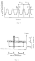
- Fig. 6 shows a performance of density projection of X-axis and Y-axis using masks.
- Fig. 7 shows a perspective view of an apparatus used for the inspection method of this invention.
- Fig. 8 shows a flow chart to explain the second embodiment.
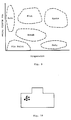
- Fig. 9 shows the kinds of defects according to the two dimensional statistics value and the variance.
- Fig. 10 shows a spots defect.
- Fig. 11 shows a blot defect.
- Fig. 12 shows a break defect.
- Fig. 13 shows a pin point defect.
- Fig. 14 shows a hole defect.
- a reference part without defect is extracted first from the liquid crystal panel.
- the way for the judgment if it is defective or defectless is many.
- there is a way to judge a part if it is defective or not which selects the parts group with maximal number of members among groups classified according to characteristics value after selecting a plurality of parts and comparing the characteristics value of them. This is based on the inventors' experience that the defective part is less then a several percent of all parts.
- the selection of the reference part and each part to be inspected can be practiced by the methods below.
- the vector data of it is generated.
- a contour of a liquid crystal part is straight lines generally, a precise figure can be reproduced with a little data by vectorizing it.
- the characteristic point of the part is appropriate for the start point, such as a convex or concave corner of a rather big right angle (Fig. 1).
- the convex or concave corner of a right angle can be extracted by generating a density projection on the location of the characteristic point (candidate location, hereinafter) as shown in Fig. 2, and calculating the minimal point of it.
- the location with the most convex or concave corners is judged to be the convex corner or the concave corner finally.
- Candidate locations are calculated by the following steps. i) The density projection is performed as to differentiated values in an image including plural parts. ii) The maximal value is obtained. iii) The candidate locations are found out in the search area by searching them by the distance of parts arrangement from the start point of the maximal value, because liquid crystal parts of the same size are arranged by the same distance. The size of the search area is decided by experience.
- step 201 rather wide area including plural parts is inputted as an image on step 201.
- the size of the area is decided by the process speed of the device and the capacity for holding data at a time. Therefore, one block for the processing is to be the area corresponding to the capacity for the process unit if high speed processing is expected by parallel processing.
- step 202 density projection in X-direction and Y-direction in each image inputted on step 201 is calculated. As the density projection data probably contains noise, smoothing is performed to each density projection data on step 203.
- step 204 density projection data reduced noise is differentiated.
- the data through step 204 is performed smoothing for further reduction of noise on step 205.
- step 206 calculating the mode (the value with the most frequency) of the data obtained after step 205, the coordinates of the mode is defined as the contour of a part.
- Parts of liquid crystal panel is arranged by the same distance and the distance can be known beforehand.
- a contour is found on step 206, other contours are searched from the starting point of the contour defining the first contour as the starting point on step 207.
- the search area is decided beforehand by experience.
- the contours appear by the distance of ⁇ L and the search area is ⁇ D
- the area within the distance from a start point of ⁇ L ⁇ D/2 is searched on step 208.
- the location with the maximal differential value is judged to be the contour (Fig. 5).
- the start point matrix can be calculated by it (step 209).
- the second contour and contours after it are all searched from the start point of the first contour, or they are searched sequentially the adjacent contour from the start point of the first found-out contour.
- method 2 detects the contour of every part and extracts it.
- the object for the judgment to extract a contour is density change pattern in gray image in the case of extracting a contour.
- lines of a contour of a part are all horizontal or vertical and are also low density, the minimal value of the density if obtained tracing the image in horizontal and vertical direction.
- Three kinds of patterns are adopted for the patterns of density change which show the minimal value. That is, the location of density decrease direction (trough starting point), the location of the minimal density (the middle trough point) and the location of density increase direction (trough ending point).
- the mean density is calculated between an indicative candidate and the next one, and whether the indicative candidate is true indication or not is judged according to the comparison of the mean density and the minimal density within the section of the adjacent indicative candidates.
- the mean density is "Dm”
- the minimal density is "dm”
- the coefficient calculated by experience is "K”
- the following formula is satisfied, it is judged that a true trough exists in the segment.
- step 301 an image is inputted in the same way on step 201 in Fig. 2.
- Density projections in the horizontal direction and in the vertical direction are generated concerning to each part in this image, and the contour of a part is extracted according to the density projection next.
- Density projection in the horizontal direction is executed on step 302, and the one in the vertical direction is executed on step 303.
- the long mask is used for the density projection in horizontal direction and wide mask is used for the one in vertical direction. Using such masks, a contour extraction according to partial characteristic is possible (Fig. 6).
- step 304 calculating the "trough starting point", "middle trough point” and “trough ending point” are calculated and they are stored once.
- the mean density (Dm) and the minimal density (dm) between the characteristic points are calculated.
- step 305 and formula (1) is performed on step 306.
- the true trough is obtained according to the calculation on step 307.
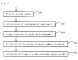
- the reference part can be extracted through the processings of flow chart in Fig. 4.
- a plurality of parts are extracted by the method mentioned above on step 401 and the histogram of each part is calculated on step 402.
- the normal part can be extracted by classifying into groups according to the histogram.
- the normal parts probably belong to the group with maximal number of members. That is, settling any number of the sample parts, the normal parts from the maximal number of group. Therefore, choosing the group with maximal number on step 404, a part is to be selected from among the members of the maximal number of group on step 405 so as to pick a normal part.
- method 2 it is possible for method 2 to extract a part easily according to vector data when only one point on the contour of a part to be extracted is picked up after generating vector data of a contour according to the method, because the method extracts the contour of a part precisely. Performing this processing to all parts of a panel to be inspected in this way, reference part and other parts are extracted.
- a part is judged if it is defective or not by comparing the histograms and other characteristic data of the reference part and each part of the liquid crystal panel between.
- Fig. 8 The process is shown in Fig. 8. the image of each part of a liquid crystal panel to be inspected is inputted by a camera and the histogram of the image is calculated on step 101. The histogram is compared with that of a defectless part on step 102. It is possible to judge if a defect part exists or not in a liquid crystal panel to be inspected by the comparison.
- the liquid crystal panel to be inspected without defective part is judged to be a good panel (on step 103). Reversely, a liquid crystal panel to be inspected with a defective part is judged to be a defective panel. The defective panel is further inspected what kind of defective part exists in it.
- the kind of the defective part is classified into five, as mentioned. It is clear by experience that each kind of defect has each characteristic distribution of the two dimensional statistics value of the histogram.
- the representative density and variance are used as the two dimensional statistics value.
- the mean value or the middle value is used as the representative density, for example.
- each part of a liquid crystal panel has fixed figure and fixed material. Therefore, when an image of a part is inputted by a camera and the histogram of the image is calculated, pixels of a normal part converges at a particular brightness.
- the brightness of the defect has a peak because the brightness of the defective part is different from that of the normal part.
- the brightness has wide variance because the brightness on the area of the defect makes a large difference.
- the brightness on the area of the defect makes a small variance because it converges on a value.
- the brightness of a defect part of a blot and a break is little different from that of a normal one.
- the distribution shows a peak neighbor the peak of the histogram of a normal part.
- the variance of those defect part is larger than a hole and smaller than a spot. That is, though there is little difference between the variance of a blot and a break, the middle value of a blot is larger than that of a break.
- the two-dimensional statistics value has two area of the variance.
- FIG. 7 shows an apparatus used for the present invention.
- a liquid crystal panel 11 is located inside of a support frame 12 so as to fixed on the frame 12 with bolt 13.
- Support frame 12 movable mounted on a pair of rails 15 on a movable plate 14.
- a cylinder device 16 is fixed on the end of movable plate 14, whose piston rod 17 is connected with the support frame 12.
- Movable plate 14 is movably mounted on a pair of rails 22 on fixed plate 21.
- the fixed plate 21 is provided with a cylinder device 23 at one end whose piston rod 24 is connected with the movable plate 14.
- Cylinder devices 16 and 23 are driven by drive circuits 25 and 26, respectively, so as to move the piston rods 17 and 24 forward or backward.
- Drive circuits 25 and 26 controlled by a control circuit 27.
- a microscope 31 is supported by a fixed frame not shown above the liquid crystal panel 11. Each pattern is inputted through the microscope 31, as described later. The image of this pattern is inputted to image processing system 32 and various processings are performed therein. Image processing system 32 is controlled by computer 33.
- LIght source 34 such as stroboscope, is provided for lighting the support frame 12 above. It is fixed to support frame 12 and move with it. Light source 34 is driven by a drive circuit 35 which is controlled by control circuit 27.
Landscapes
- Physics & Mathematics (AREA)
- Health & Medical Sciences (AREA)
- Life Sciences & Earth Sciences (AREA)
- Chemical & Material Sciences (AREA)
- Analytical Chemistry (AREA)
- Biochemistry (AREA)
- General Health & Medical Sciences (AREA)
- General Physics & Mathematics (AREA)
- Immunology (AREA)
- Pathology (AREA)
- Testing Of Optical Devices Or Fibers (AREA)
- Liquid Crystal (AREA)
- Investigating Materials By The Use Of Optical Means Adapted For Particular Applications (AREA)
Applications Claiming Priority (4)
| Application Number | Priority Date | Filing Date | Title |
|---|---|---|---|
| JP1587891A JPH04313041A (ja) | 1991-01-16 | 1991-01-16 | 液晶パネルの検査方法 |
| JP15878/91 | 1991-01-16 | ||
| JP2393591A JPH04348316A (ja) | 1991-01-24 | 1991-01-24 | 液晶パネルの検査方法 |
| JP23935/91 | 1991-01-24 |
Publications (2)
| Publication Number | Publication Date |
|---|---|
| EP0495481A2 true EP0495481A2 (de) | 1992-07-22 |
| EP0495481A3 EP0495481A3 (en) | 1993-06-02 |
Family
ID=26352106
Family Applications (1)
| Application Number | Title | Priority Date | Filing Date |
|---|---|---|---|
| EP19920100604 Withdrawn EP0495481A3 (en) | 1991-01-16 | 1992-01-15 | Liquid crystal panel inspection method |
Country Status (2)
| Country | Link |
|---|---|
| US (1) | US5394481A (de) |
| EP (1) | EP0495481A3 (de) |
Families Citing this family (9)
| Publication number | Priority date | Publication date | Assignee | Title |
|---|---|---|---|---|
| JP3297950B2 (ja) * | 1993-07-13 | 2002-07-02 | シャープ株式会社 | 平面型表示パネル検査装置 |
| JPH09326026A (ja) * | 1996-06-07 | 1997-12-16 | Advantest Corp | 画像処理方法及び画像処理装置 |
| US6009187A (en) * | 1996-12-02 | 1999-12-28 | Motorola, Inc. | Wafer prober having an emissive display inspection system and method of use |
| US6757421B1 (en) * | 2000-09-27 | 2004-06-29 | Cognex Corporation | Method and apparatus for detecting defects |
| US20050286753A1 (en) * | 2004-06-25 | 2005-12-29 | Triant Technologies Inc. | Automated inspection systems and methods |
| TW200700799A (en) * | 2005-06-24 | 2007-01-01 | Innolux Display Corp | Testing system of liquid crystal display |
| US8867817B1 (en) | 2012-10-29 | 2014-10-21 | Amazon Technologies, Inc. | Display analysis using scanned images |
| EP3186732B1 (de) | 2014-08-29 | 2021-11-10 | Microsoft Technology Licensing, LLC | Herstellung dreidimensionaler gegenstände |
| WO2018071041A1 (en) * | 2016-10-14 | 2018-04-19 | Hewlett-Packard Development Company, L.P. | Rebuilding three-dimensional models to provide simplified three-dimensional models |
Family Cites Families (14)
| Publication number | Priority date | Publication date | Assignee | Title |
|---|---|---|---|---|
| US3803553A (en) * | 1972-06-14 | 1974-04-09 | Hitachi Ltd | Character recognition apparatus |
| US4213117A (en) * | 1977-11-28 | 1980-07-15 | Hitachi, Ltd. | Method and apparatus for detecting positions of chips on a semiconductor wafer |
| US4589139A (en) * | 1982-02-04 | 1986-05-13 | Nippon Kogaku K. K. | Apparatus for detecting defects in pattern |
| US4606065A (en) * | 1984-02-09 | 1986-08-12 | Imaging Technology Incorporated | Image processing-system |
| US4648053A (en) * | 1984-10-30 | 1987-03-03 | Kollmorgen Technologies, Corp. | High speed optical inspection system |
| US4783828A (en) * | 1986-06-02 | 1988-11-08 | Honeywell Inc. | Two-dimensional object recognition using chain codes, histogram normalization and trellis algorithm |
| JP2603946B2 (ja) * | 1986-09-26 | 1997-04-23 | オリンパス光学工業株式会社 | 画像間の対応領域の検出装置 |
| US5073952A (en) * | 1988-09-07 | 1991-12-17 | Sigmax Kabushiki Kaisha | Pattern recognition device |
| JPH0638274B2 (ja) * | 1989-07-31 | 1994-05-18 | 工業技術院長 | 画像認識装置および画像認識方法 |
| US4943732A (en) * | 1989-08-16 | 1990-07-24 | Micrion Corporation | Method and apparatus for defect detection and location |
| JP3132565B2 (ja) * | 1989-08-30 | 2001-02-05 | 株式会社日立製作所 | 欠陥検査方法及びその装置 |
| JP3187827B2 (ja) * | 1989-12-20 | 2001-07-16 | 株式会社日立製作所 | パターン検査方法および装置 |
| US5185812A (en) * | 1990-02-14 | 1993-02-09 | Kabushiki Kaisha Toshiba | Optical pattern inspection system |
| JPH04158238A (ja) * | 1990-10-22 | 1992-06-01 | Ezel Inc | 液晶パネルの検査方法 |
-
1992
- 1992-01-15 EP EP19920100604 patent/EP0495481A3/en not_active Withdrawn
- 1992-01-15 US US07/820,925 patent/US5394481A/en not_active Expired - Fee Related
Also Published As
| Publication number | Publication date |
|---|---|
| US5394481A (en) | 1995-02-28 |
| EP0495481A3 (en) | 1993-06-02 |
Similar Documents
| Publication | Publication Date | Title |
|---|---|---|
| CN114881987B (zh) | 基于改进YOLOv5的热压导光板缺陷可视化检测方法 | |
| KR100474571B1 (ko) | 웨이퍼의 패턴 검사용 기준 이미지 설정 방법과 이 설정방법을 이용한 패턴 검사 방법 및 장치 | |
| CN103913468B (zh) | 生产线上大尺寸lcd玻璃基板的多视觉缺陷检测设备及方法 | |
| US5204910A (en) | Method for detection of defects lacking distinct edges | |
| US4845763A (en) | Tool wear measurement by machine vision | |
| EP1254431B1 (de) | Verfahren und system zur aufspürung von fehlern auf einer gedruckten leiterplatte | |
| CN113034464B (zh) | 一种多背景下的液晶显示器缺陷视觉实时检测方法 | |
| CN119006503B (zh) | 基于纹理特征分析的接触式仪器三维轮廓缺陷检测方法 | |
| CN115620061B (zh) | 一种基于图像识别技术的五金零件缺陷检测方法及系统 | |
| CN120182258B (zh) | 基于图像识别的线路板微孔镀铜品质检验方法 | |
| CN119991544B (zh) | 基于二维图像的输电线路耐张线夹缺陷智能分类方法与系统 | |
| US5204617A (en) | Liquid crystal panel inspection method | |
| US5394481A (en) | Liquid crystal panel inspection method | |
| CN115471486A (zh) | 一种交换机接口完好性检测方法 | |
| CN115393290B (zh) | 边缘缺陷检测方法、装置及设备 | |
| CN114037682A (zh) | 一种光学元件表面疵病二维自动检测方法 | |
| CN120102589A (zh) | 触摸屏的表面缺陷检测方法及相关设备 | |
| Feng et al. | Image processing of the grinding wheel surface | |
| CN114881952A (zh) | 一种铸件缺陷区域检测及边缘准确分割方法 | |
| Dong et al. | A New Method for Rapid Detection of Surface Defects on Complex Textured Tiles | |
| CN121391774A (zh) | 布匹瑕疵检测方法、装置、设备及存储介质 | |
| CN118097305B (zh) | 一种半导体发光元件质量的检测方法及系统 | |
| CN111833350A (zh) | 机器视觉检测方法与系统 | |
| Suetens et al. | Critical review of visual inspection | |
| CN118961755B (zh) | 一种基于机器学习的led线路板自动缺陷识别方法 |
Legal Events
| Date | Code | Title | Description |
|---|---|---|---|
| PUAI | Public reference made under article 153(3) epc to a published international application that has entered the european phase |
Free format text: ORIGINAL CODE: 0009012 |
|
| AK | Designated contracting states |
Kind code of ref document: A2 Designated state(s): BE DE FR GB IT NL SE |
|
| PUAL | Search report despatched |
Free format text: ORIGINAL CODE: 0009013 |
|
| AK | Designated contracting states |
Kind code of ref document: A3 Designated state(s): BE DE FR GB IT NL SE |
|
| 17P | Request for examination filed |
Effective date: 19930505 |
|
| RAP1 | Party data changed (applicant data changed or rights of an application transferred) |
Owner name: EZEL INC. Owner name: SHARP KABUSHIKI KAISHA |
|
| RAP1 | Party data changed (applicant data changed or rights of an application transferred) |
Owner name: SHARP KABUSHIKI KAISHA Owner name: EZEL INC. |
|
| RAP3 | Party data changed (applicant data changed or rights of an application transferred) |
Owner name: SHARP KABUSHIKI KAISHA Owner name: EZEL INC. |
|
| RAP1 | Party data changed (applicant data changed or rights of an application transferred) |
Owner name: YOZAN INC. Owner name: SHARP KABUSHIKI KAISHA |
|
| 17Q | First examination report despatched |
Effective date: 19970226 |
|
| STAA | Information on the status of an ep patent application or granted ep patent |
Free format text: STATUS: THE APPLICATION IS DEEMED TO BE WITHDRAWN |
|
| 18D | Application deemed to be withdrawn |
Effective date: 19980801 |