EP0495573A2 - Spannungsgesteuerter CMOS-Oszillator - Google Patents
Spannungsgesteuerter CMOS-Oszillator Download PDFInfo
- Publication number
- EP0495573A2 EP0495573A2 EP92300100A EP92300100A EP0495573A2 EP 0495573 A2 EP0495573 A2 EP 0495573A2 EP 92300100 A EP92300100 A EP 92300100A EP 92300100 A EP92300100 A EP 92300100A EP 0495573 A2 EP0495573 A2 EP 0495573A2
- Authority
- EP
- European Patent Office
- Prior art keywords
- current
- channel
- signal
- voltage
- output signal
- Prior art date
- Legal status (The legal status is an assumption and is not a legal conclusion. Google has not performed a legal analysis and makes no representation as to the accuracy of the status listed.)
- Withdrawn
Links
Images


Classifications
-
- H—ELECTRICITY
- H03—ELECTRONIC CIRCUITRY
- H03K—PULSE TECHNIQUE
- H03K3/00—Circuits for generating electric pulses; Monostable, bistable or multistable circuits
- H03K3/02—Generators characterised by the type of circuit or by the means used for producing pulses
- H03K3/353—Generators characterised by the type of circuit or by the means used for producing pulses by the use, as active elements, of field-effect transistors with internal or external positive feedback
- H03K3/354—Astable circuits
-
- G—PHYSICS
- G05—CONTROLLING; REGULATING
- G05F—SYSTEMS FOR REGULATING ELECTRIC OR MAGNETIC VARIABLES
- G05F3/00—Non-retroactive systems for regulating electric variables by using an uncontrolled element, or an uncontrolled combination of elements, such element or such combination having self-regulating properties
- G05F3/02—Regulating voltage or current
- G05F3/08—Regulating voltage or current wherein the variable is DC
- G05F3/10—Regulating voltage or current wherein the variable is DC using uncontrolled devices with non-linear characteristics
- G05F3/16—Regulating voltage or current wherein the variable is DC using uncontrolled devices with non-linear characteristics being semiconductor devices
- G05F3/20—Regulating voltage or current wherein the variable is DC using uncontrolled devices with non-linear characteristics being semiconductor devices using diode- transistor combinations
- G05F3/24—Regulating voltage or current wherein the variable is DC using uncontrolled devices with non-linear characteristics being semiconductor devices using diode- transistor combinations wherein the transistors are of the field-effect type only
- G05F3/242—Regulating voltage or current wherein the variable is DC using uncontrolled devices with non-linear characteristics being semiconductor devices using diode- transistor combinations wherein the transistors are of the field-effect type only with compensation for device parameters, e.g. channel width modulation, threshold voltage, processing, or external variations, e.g. temperature, loading, supply voltage
- G05F3/247—Regulating voltage or current wherein the variable is DC using uncontrolled devices with non-linear characteristics being semiconductor devices using diode- transistor combinations wherein the transistors are of the field-effect type only with compensation for device parameters, e.g. channel width modulation, threshold voltage, processing, or external variations, e.g. temperature, loading, supply voltage producing a voltage or current as a predetermined function of the supply voltage
-
- H—ELECTRICITY
- H03—ELECTRONIC CIRCUITRY
- H03K—PULSE TECHNIQUE
- H03K3/00—Circuits for generating electric pulses; Monostable, bistable or multistable circuits
- H03K3/01—Details
- H03K3/011—Modifications of generator to compensate for variations in physical values, e.g. voltage, temperature
-
- H—ELECTRICITY
- H03—ELECTRONIC CIRCUITRY
- H03L—AUTOMATIC CONTROL, STARTING, SYNCHRONISATION OR STABILISATION OF GENERATORS OF ELECTRONIC OSCILLATIONS OR PULSES
- H03L7/00—Automatic control of frequency or phase; Synchronisation
- H03L7/06—Automatic control of frequency or phase; Synchronisation using a reference signal applied to a frequency- or phase-locked loop
- H03L7/08—Details of the phase-locked loop
- H03L7/099—Details of the phase-locked loop concerning mainly the controlled oscillator of the loop
- H03L7/0995—Details of the phase-locked loop concerning mainly the controlled oscillator of the loop the oscillator comprising a ring oscillator
Definitions
- the present invention relates to voltage-controlled oscillators and, in particular, to methods and apparatus for obtaining a variable clock frequency having a well-controlled output range and duty cycle over varying temperature, process and supply voltage.
- a basic phase-locked loop (PLL) system 10 includes three essential elements - a phase detector 12, a loop filter 14 and a voltage-controlled oscillator (VCO) 16 - interconnected to form a feedback system.
- the phase detector 12 compares the phase of the input signal V s (t) with the output frequency V o (t) of the VCO 16 and generates an error voltage V d (t) corresponding to the difference.
- the error voltage signal V d (t) is then filtered by the loop filter 14 and applied to the control terminal of the VCO 16 in the form of an error voltage V e (t) to control its frequency of oscillation.
- the VCO 16 is the most critical element of the PLL system 10.
- the tuning slope that is, the output frequency V o (t) dependence on control voltage V e (t) is determined by the conversion gain constant K VCO of the VCO 16.
- the linearity of the voltage-to-frequency conversion characteristics of the PLL system 10 is determined solely by the limitations of the control characteristics of the VCO 16.
- the stability and control characteristics of the VCO 16 are key design parameters in monolithic PLL circuits.
- the VCO 16 which is basically an analog circuit, must be immune to on-chip and off-chip noise sources. If it is not, then its output V o (t) will exhibit short-term frequency instability, or jitter. Maintaining a low VCO gain constant K VCO is one method of reducing noise sensitivity.
- the required operating frequency for conventional VCOs ranges from a few MHz to beyond 200 MHz. Tuning ranges up to 2 to 1 are also required. To be easily compatible with 5V power supply constraints and minimum phase detector/charge pump solutions, the tuning voltage should be approximately 1.5V to (V cc -1.5V).
- VCO gain constant K VCO must be well controlled so that loop filtering schemes are predictable and stable. This is especially important in data acquisition and mass storage applications such as disk controllers and constant density recording. At higher output frequencies, the duty cycle is also critical.
- CMOS complementary-metal-oxide-semiconductor
- Ware et al "a 200MHz CMOS Phase-Lock-Loop with Dual Phase Detectors", IEEE Transactions on Solid State Circuits, May 10, 1989.
- the Ware et al PLL features a VCO that requires the use of a bandgap regulator that relies on parasitic NPN transistors. It achieves frequency control by varying the applied voltage across the ring oscillator stages.
- the VCO utilized by Ware is based on a ring of three inverting amplifiers.
- the present invention provides a high frequency CMOS voltage controlled oscillator circuit with gain constant and duty cycle compensation.
- the voltage controlled oscillator circuit includes a multi-stage ring oscillator that includes a plurality of series-connected inverter stages comprising N-channel and P-channel transistors.
- the ring oscillator responds to a control current signal for controlling the frequency of oscillation of the ring oscillator.
- a voltage-to-current converter converts a tuning voltage input signal to a corresponding output current signal that is independent of the channel strength of the N-channel and P-channel transistors.
- Process compensation circuitry responds to the tuning voltage input signal to provide a current dump output signal corresponding to the channel strength of the P-channel and N-channel transistors.
- Trip-point compensation circuit provides a net ring current signal as the current control signal to the ring oscillator. The net ring current signal represents the difference between the output current signal and the current dump output signal.
- Fig. 1 is a block diagram illustrating the basic elements of a conventional phase-locked loop (PLL).
- PLL phase-locked loop
- Fig. 2 is a block diagram illustrating an embodiment of voltage-controlled oscillator (VCO) in accordance with the present invention.
- VCO voltage-controlled oscillator
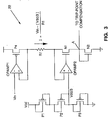
- Fig. 3 is a schematic diagram illustrating an embodiment of a V/I converter utilizable in the VCO shown in Fig. 2.
- Fig. 4 is a schematic diagram illustrating an embodiment of ring trip-point compensation circuitry together with a conventional ring oscillator utilizable in the VCO shown in Fig. 2.
- Fig. 4A is a schematic diagram illustrating a generalized representation of the Fig. 4 circuit.
- Fig. 5 is a schematic diagram illustrating an embodiment of process compensation circuitry utilizable in the VCO shown in Fig. 2.
- Fig. 6 is a graph illustrating VCO frequency versus process and operating conditions for a VCO in accordance with the present invention.
- Fig. 2 shows a block diagram of a CMOS voltage-controlled oscillator (VCO) 20 with gain constant and duty cycle compensation in accordance with the present invention.
- VCO voltage-controlled oscillator
- VCO 20 includes a voltage-to-current V/I converter 22 with gain Gm that amplifies input signal V in to current mirror and trip-point compensation circuitry 24.
- the outputs of the trip-point compensation circuitry 24 are provided to a CMOS ring oscillator 26.
- the selected phase signal of the ring oscillator 26 is provided as the VCO output via an output buffer 28.
- the VCO 20 includes process and temperature compensation for the V/I converter 22 and process compensation for the trip-point circuitry 24. Duty cycle compensation for both the trip-point balance circuitry 24 and the output buffer 28 is derived from matching devices within these two circuit elements.
- FIG. 3 An embodiment of a V/I converter 22 utilizable in the VCO 20 is shown in greater detail in Fig. 3.
- tuning voltage input signal V in is provided to the inverting input of operational amplifier OPAMP1.
- the non-inverting input of op amp OPAMP1 is connected to the drain of P-channel transistor P4 which is driven by the output of op amp OPAMP1.
- a second operational amplifier OPAMP2 drives N-channel sense transistor N1, which has its source connected to an output node A.
- the non-inverting input of op amp OPAM2 is connected to the drain of P-channel sense transistor P4 via internal current control resistor R1.
- the inverting input of op amp OPAMP2 is connected to receive a V DD driver stage output, the driver stage comprising three series-connected, P-channel transistors P1, P2 and P3 which are connected between a supply voltage V DD and ground.
- An N-channel output mirror transistor N2 is connected between the output node A and ground.
- the output current at node A of the V/I converter 22 is controlled by forcing the bottom side of resistor R1 to V DD /3 and the top side of resistor R1 to V in .
- the transconductance slope is totally independent of supply V DD .
- Resistor R1 can also be an external component for even greater accuracy. In this case, both external connections are floating above ground and external noise can be made common-mode.
- the current at node A is then mirrored into the ring oscillator 26, as described below.
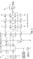
- FIG. 4 An embodiment of current mirror and ring trippoint compensation circuitry 24 is shown in greater detail in Fig. 4.
- Trip-point compensation is desirable in order to maintain symmetric VCO output waveforms as the process varies. For example, when the process tends toward weak N-channel and strong P-channel transistors, the resultant VCO output waveform will have a higher duty cycle than when the N-channel and P-channel transistor strengths are well matched.
- the Fig. 4 circuit includes a differential stage, comprising N-channel transistors N4 and N5, that allows the total ring oscillator current from the V/I converter 22 to be shared as process shift demands. That is, as the P-channel transistors of the VCO get weaker because of process variation, the self-biased inverter (transistors P10 and N8) voltage in the Fig. 4 circuit will tend to drop, forcing more current to be steered through input transistor N4 and then mirrored from P-channel transistor P6 to P-channel current sensing transistors P9, P11, P13 and P15. Similarly, when the N-channel transistors get weaker, more current is steered through P-channel input transistor P7 and mirrored into transistors P8 and N7 and current sensing transistors N9, N11, N13 and N15.
- the ring trip-point compensation circuitry includes a dummy inverter stage (transistors P10 and N8) that is identical in form to the three inverter stages (P12/N10, P14/N12 and P16/N14) of the ring oscillator.
- the ring oscillator is a standard design having an output frequency equal to 1/6T, where T is the propagation delay of an inverter (P12/N10, P14/N12, P16/N14).
- Fig. 4 circuitry can be more generally illustrated as shown in Fig. 4A. That is, as shown in Fig. 4A, the amplified V/I converter control input received from buffer Gm drives a first current I1. The current dump from the process compensation circuitry drives a second current source I2. The net ring oscillator current equals the V/I current I1 minus the process compensation current I2.
- the compensation circuit 24 uses a self-biased inverter 30 comprising P-channel transistor P5 and N-channel transistor N3 to drive the ring oscillator bias such that the resultant oscillation is also matched with the output buffer G1.
- Output buffer G1 amplifies and squares the ring oscillator signal.
- the process compensation circuit maintains a constant frequency tuning range over process variations such as transistor threshold voltage, transconductance and source/drain capacitance. It also compensates for externally induced variations, such as temperature and supply voltage V DD .
- a V DD voltage splitter stage consisting of P-channel transistors P17, P18 and P19 sets up a V DD -dependent gate bias on P-channel transistor P20 and N-channel transistor N20.
- P-channel strength increases, the currents in N-channel sensing transistors N16 and N17 increase proportionally.
- N-channel strength increases, the current in N-channel sensing transistor N20 increases.
- the P-channel and N-channel strength-dependent currents sum to become the tail current in the differential stage comprising N-channel transistors N18 and N19, which is part of a K VCO compression network.
- Fig. 6 provides a plot of VCO frequency versus process and operating conditions based on a SPICE simulation of the concepts of the invention described above for a 5V integrated circuit under worst case operating conditions.
- the simulation indicates that VCO gain constant (K VCO ) compression of approximately 2:1 is possible.
- Conventional VCO designs exhibit gain constant compression of 3.5:1 or more.
Landscapes
- Engineering & Computer Science (AREA)
- Microelectronics & Electronic Packaging (AREA)
- Physics & Mathematics (AREA)
- Nonlinear Science (AREA)
- Electromagnetism (AREA)
- General Physics & Mathematics (AREA)
- Radar, Positioning & Navigation (AREA)
- Automation & Control Theory (AREA)
- Stabilization Of Oscillater, Synchronisation, Frequency Synthesizers (AREA)
Applications Claiming Priority (2)
| Application Number | Priority Date | Filing Date | Title |
|---|---|---|---|
| US07/642,677 US5061907A (en) | 1991-01-17 | 1991-01-17 | High frequency CMOS VCO with gain constant and duty cycle compensation |
| US642677 | 1991-01-17 |
Publications (2)
| Publication Number | Publication Date |
|---|---|
| EP0495573A2 true EP0495573A2 (de) | 1992-07-22 |
| EP0495573A3 EP0495573A3 (en) | 1993-01-13 |
Family
ID=24577563
Family Applications (1)
| Application Number | Title | Priority Date | Filing Date |
|---|---|---|---|
| EP19920300100 Withdrawn EP0495573A3 (en) | 1991-01-17 | 1992-01-07 | Cmos voltage controlled oscillator |
Country Status (3)
| Country | Link |
|---|---|
| US (1) | US5061907A (de) |
| EP (1) | EP0495573A3 (de) |
| JP (1) | JPH0514136A (de) |
Cited By (4)
| Publication number | Priority date | Publication date | Assignee | Title |
|---|---|---|---|---|
| DE19728248C2 (de) * | 1996-12-30 | 1999-09-23 | Lg Semicon Co Ltd | Spannungsgesteuerter Oszillator |
| US6005444A (en) * | 1996-09-25 | 1999-12-21 | Nokia Telecommunications Oy | Circuits for producing control currents for a current controlled oscillator |
| EP0866555A3 (de) * | 1997-03-17 | 2000-04-19 | Sony Corporation | Verzögerungsschaltung und Oszillator unter Verwendung derselben |
| EP0921640A3 (de) * | 1997-12-03 | 2002-09-18 | Nec Corporation | Spannungsgesteuerte Oszillatorschaltung |
Families Citing this family (89)
| Publication number | Priority date | Publication date | Assignee | Title |
|---|---|---|---|---|
| US5175512A (en) * | 1992-02-28 | 1992-12-29 | Avasem Corporation | High speed, power supply independent CMOS voltage controlled ring oscillator with level shifting circuit |
| US5302888A (en) * | 1992-04-01 | 1994-04-12 | Texas Instruments Incorporated | CMOS integrated mid-supply voltage generator |
| FI92120C (fi) * | 1992-04-15 | 1994-09-26 | Nokia Mobile Phones Ltd | Jänniteohjattu oskillaattori |
| US5239274A (en) * | 1992-05-26 | 1993-08-24 | Digital Equipment Corporation | Voltage-controlled ring oscillator using complementary differential buffers for generating multiple phase signals |
| US5285173A (en) * | 1992-07-13 | 1994-02-08 | Analog Devices, Inc. | Signal-controlled ring oscillator with delay cells having constant gain with change in frequency |
| US5317287A (en) * | 1992-07-16 | 1994-05-31 | National Semiconductor Corporation | Low-gain, range programmable, temperature compensated voltage controlled ring oscillator |
| JPH06152334A (ja) * | 1992-11-06 | 1994-05-31 | Mitsubishi Electric Corp | リングオシレータおよび定電圧発生回路 |
| US5278522A (en) * | 1992-11-19 | 1994-01-11 | Codex, Corp. | High frequency voltage controlled oscillator |
| US5811998A (en) * | 1993-01-28 | 1998-09-22 | Digital Equipment Corporation | State machine phase lock loop |
| US5331295A (en) * | 1993-02-03 | 1994-07-19 | National Semiconductor Corporation | Voltage controlled oscillator with efficient process compensation |
| JPH06343022A (ja) * | 1993-06-01 | 1994-12-13 | Fujitsu Ltd | 電圧制御発振回路 |
| US5442325A (en) * | 1993-10-08 | 1995-08-15 | Texas Instruments Incorporated | Voltage-controlled oscillator and system with reduced sensitivity to power supply variation |
| US5576666A (en) * | 1993-11-12 | 1996-11-19 | Nippondenso Technical Center Usa, Inc. | Fractional-N frequency synthesizer with temperature compensation |
| DE4341221A1 (de) * | 1993-12-03 | 1995-06-08 | Thomson Brandt Gmbh | Anordnung zur Verringerung von Störungen bei Schwingkreisen in integrierten Schaltungen |
| US5485126A (en) * | 1994-01-25 | 1996-01-16 | International Business Machines Corporation | Ring oscillator circuit having output with fifty percent duty cycle |
| US5559477A (en) * | 1994-02-10 | 1996-09-24 | International Microcircuits, Inc. | Pulse generator having controlled delay to control duty cycle |
| US5550495A (en) * | 1994-05-12 | 1996-08-27 | Sierra Semiconductor Corporation | All MOS voltage to current converter |
| US5471176A (en) * | 1994-06-07 | 1995-11-28 | Quantum Corporation | Glitchless frequency-adjustable ring oscillator |
| JP2755181B2 (ja) * | 1994-08-12 | 1998-05-20 | 日本電気株式会社 | 電圧制御発振器 |
| US5426398A (en) * | 1994-08-19 | 1995-06-20 | National Semiconductor Corporation | High speed differential mode voltage controlled ring oscillator |
| US5463352A (en) * | 1994-09-23 | 1995-10-31 | At&T Global Information Solutions Company | Supply voltage tolerant phase-locked loop circuit |
| DE19655128C2 (de) * | 1995-02-06 | 2001-10-31 | Mitsubishi Electric Corp | Halbleitereinrichtung |
| JP3523718B2 (ja) | 1995-02-06 | 2004-04-26 | 株式会社ルネサステクノロジ | 半導体装置 |
| JP3780030B2 (ja) * | 1995-06-12 | 2006-05-31 | 株式会社ルネサステクノロジ | 発振回路およびdram |
| JP3862306B2 (ja) * | 1995-06-23 | 2006-12-27 | 三菱電機株式会社 | 半導体装置 |
| GB9522223D0 (en) * | 1995-10-31 | 1996-01-03 | Sgs Thomson Microelectronics | A circuit for generating an output signal having a 50% duty cycle |
| KR0172758B1 (ko) * | 1995-12-29 | 1999-03-30 | 김주용 | 주파수의 주기조절이 가능한 주파수발생기 |
| US5994937A (en) * | 1996-11-06 | 1999-11-30 | International Business Machines Corporation | Temperature and power supply adjusted address transition detector |
| US5847616A (en) * | 1996-12-12 | 1998-12-08 | Tritech Microelectronics International, Ltd. | Embedded voltage controlled oscillator with minimum sensitivity to process and supply |
| US5905412A (en) * | 1997-05-21 | 1999-05-18 | National Semiconductor Corporation | Process compensation method for CMOS current controlled ring oscillators |
| US5892409A (en) * | 1997-07-28 | 1999-04-06 | International Business Machines Corporation | CMOS process compensation circuit |
| SE515783C2 (sv) * | 1997-09-11 | 2001-10-08 | Ericsson Telefon Ab L M | Elektriska anordningar jämte förfarande för deras tillverkning |
| US6157266A (en) * | 1998-02-12 | 2000-12-05 | Hewlett-Packard Company | Delay elements arranged for a signal controlled oscillator |
| US6060922A (en) * | 1998-02-20 | 2000-05-09 | Industrial Technology Research Institute | Duty cycle control buffer circuit with selective frequency dividing function |
| DE19822373C2 (de) * | 1998-02-20 | 2001-05-31 | Ind Technology Res Inst Hsinch | Frequenzvervielfachungsschaltung und -verfahren |
| US6326855B1 (en) * | 1998-06-01 | 2001-12-04 | Agere Systems, Inc | Voltage-to-current converter circuit with independent and adjustable compensation for process, voltage, and temperature |
| US6094074A (en) * | 1998-07-16 | 2000-07-25 | Seiko Epson Corporation | High speed common mode logic circuit |
| US6011443A (en) * | 1998-07-16 | 2000-01-04 | Seiko Epson Corporation | CMOS voltage controlled oscillator |
| KR100329793B1 (ko) * | 1998-12-30 | 2002-05-09 | 박종섭 | 전압제어발진기 |
| US5978241A (en) * | 1999-01-28 | 1999-11-02 | Industrial Technology Research Institute | Wide-linear range tunable transconductor using MOS |
| US6097253A (en) * | 1999-02-12 | 2000-08-01 | Pmc-Sierra Ltd. | High speed process-controlled transresistance amplifier |
| US7548726B1 (en) * | 1999-10-21 | 2009-06-16 | Broadcom Corporation | Adaptive radio transceiver with a bandpass filter |
| US6353368B1 (en) * | 1999-11-09 | 2002-03-05 | Vlsi Technology, Inc. | VCO circuit using negative feedback to reduce phase noise |
| US6466100B2 (en) | 2001-01-08 | 2002-10-15 | International Business Machines Corporation | Linear voltage controlled oscillator transconductor with gain compensation |
| US6650190B2 (en) * | 2001-04-11 | 2003-11-18 | International Business Machines Corporation | Ring oscillator with adjustable delay |
| US6804502B2 (en) | 2001-10-10 | 2004-10-12 | Peregrine Semiconductor Corporation | Switch circuit and method of switching radio frequency signals |
| US6949984B2 (en) * | 2002-06-06 | 2005-09-27 | Texas Instruments Incorporated | Voltage controlled oscillator having control current compensation |
| KR100509357B1 (ko) * | 2003-08-08 | 2005-08-22 | 삼성전자주식회사 | 온도 독립형 전압 제어 발진기 및 주파수 발생 방법 |
| US7719343B2 (en) | 2003-09-08 | 2010-05-18 | Peregrine Semiconductor Corporation | Low noise charge pump method and apparatus |
| US6956420B2 (en) * | 2003-09-30 | 2005-10-18 | Intel Corporation | Duty cycle compensation in clock circuit |
| JP4659826B2 (ja) | 2004-06-23 | 2011-03-30 | ペレグリン セミコンダクター コーポレーション | Rfフロントエンド集積回路 |
| FR2882871A1 (fr) * | 2005-03-01 | 2006-09-08 | Atmel Corp | Oscillateur commande en tension a multiphase realignee et boucle a phase asservie associee |
| USRE48965E1 (en) | 2005-07-11 | 2022-03-08 | Psemi Corporation | Method and apparatus improving gate oxide reliability by controlling accumulated charge |
| US7910993B2 (en) | 2005-07-11 | 2011-03-22 | Peregrine Semiconductor Corporation | Method and apparatus for use in improving linearity of MOSFET's using an accumulated charge sink |
| US9653601B2 (en) | 2005-07-11 | 2017-05-16 | Peregrine Semiconductor Corporation | Method and apparatus for use in improving linearity of MOSFETs using an accumulated charge sink-harmonic wrinkle reduction |
| US20080076371A1 (en) | 2005-07-11 | 2008-03-27 | Alexander Dribinsky | Circuit and method for controlling charge injection in radio frequency switches |
| US7890891B2 (en) * | 2005-07-11 | 2011-02-15 | Peregrine Semiconductor Corporation | Method and apparatus improving gate oxide reliability by controlling accumulated charge |
| US8742502B2 (en) | 2005-07-11 | 2014-06-03 | Peregrine Semiconductor Corporation | Method and apparatus for use in improving linearity of MOSFETs using an accumulated charge sink-harmonic wrinkle reduction |
| US7339439B2 (en) * | 2005-07-18 | 2008-03-04 | Atmel Corporation | Voltage-controlled oscillator with multi-phase realignment of asymmetric stages |
| US7355482B2 (en) * | 2006-02-17 | 2008-04-08 | Seiko Epson Corporation | Methods and apparatus for compensating a variable oscillator for process, voltage, and temperature variations using a replica oscillator |
| JP4991193B2 (ja) * | 2006-07-04 | 2012-08-01 | 株式会社日立製作所 | 周波数可変発振器 |
| TW200820622A (en) * | 2006-10-17 | 2008-05-01 | Realtek Semiconductor Corp | Current device and method for phase-locked loop |
| DE102006061721B4 (de) * | 2006-12-28 | 2016-12-29 | Infineon Technologies Ag | Kompensationsgrößen-Bereitstellungsschaltung, Spannungs-Kompensationsschaltung, spannungskompensierte Schaltung, Vorrichtung zur Bereitstellung einer Kompensationsgröße, Verfahren zum Bereitstellen einer Kompensationsgröße und Ring-Oszillator |
| US7960772B2 (en) | 2007-04-26 | 2011-06-14 | Peregrine Semiconductor Corporation | Tuning capacitance to enhance FET stack voltage withstand |
| JP2008311862A (ja) * | 2007-06-13 | 2008-12-25 | Toshiba Corp | 電圧制御発振器及びこれを用いた位相同期回路 |
| JP2009010498A (ja) * | 2007-06-26 | 2009-01-15 | Nec Electronics Corp | 半導体回路 |
| JP5417346B2 (ja) | 2008-02-28 | 2014-02-12 | ペレグリン セミコンダクター コーポレーション | 集積回路素子内でキャパシタをデジタル処理で同調するときに用いられる方法及び装置 |
| EP2330735A3 (de) * | 2008-07-18 | 2012-04-04 | Peregrine Semiconductor Corporation | Transkonduktanz-Operationsverstärker |
| US9660590B2 (en) | 2008-07-18 | 2017-05-23 | Peregrine Semiconductor Corporation | Low-noise high efficiency bias generation circuits and method |
| US9030248B2 (en) * | 2008-07-18 | 2015-05-12 | Peregrine Semiconductor Corporation | Level shifter with output spike reduction |
| JP4641045B2 (ja) * | 2009-08-17 | 2011-03-02 | ルネサスエレクトロニクス株式会社 | 半導体集積回路及びマイクロコンピュータ |
| US8686787B2 (en) | 2011-05-11 | 2014-04-01 | Peregrine Semiconductor Corporation | High voltage ring pump with inverter stages and voltage boosting stages |
| US9264053B2 (en) | 2011-01-18 | 2016-02-16 | Peregrine Semiconductor Corporation | Variable frequency charge pump |
| US9147443B2 (en) * | 2011-05-20 | 2015-09-29 | The Regents Of The University Of Michigan | Low power reference current generator with tunable temperature sensitivity |
| US9590674B2 (en) | 2012-12-14 | 2017-03-07 | Peregrine Semiconductor Corporation | Semiconductor devices with switchable ground-body connection |
| US20150236748A1 (en) | 2013-03-14 | 2015-08-20 | Peregrine Semiconductor Corporation | Devices and Methods for Duplexer Loss Reduction |
| CN103618545A (zh) * | 2013-11-26 | 2014-03-05 | 苏州贝克微电子有限公司 | 一种高频cmos压控振荡器 |
| US9425773B2 (en) * | 2013-12-13 | 2016-08-23 | Taiwan Semiconductor Manufacturing Co., Ltd. | Digital control ring oscillator and method of assembling same |
| US9356570B2 (en) | 2014-05-15 | 2016-05-31 | Texas Instruments Deutschland Gmbh | High speed, rail-to-rail CMOS differential input stage |
| US9831857B2 (en) | 2015-03-11 | 2017-11-28 | Peregrine Semiconductor Corporation | Power splitter with programmable output phase shift |
| US9948281B2 (en) | 2016-09-02 | 2018-04-17 | Peregrine Semiconductor Corporation | Positive logic digitally tunable capacitor |
| US10425064B2 (en) * | 2016-12-08 | 2019-09-24 | Micron Technology, Inc. | Apparatus and method for a PVT independent RC delay |
| US10541688B2 (en) * | 2017-12-05 | 2020-01-21 | Bae Systems Information And Electronic Systems Integration Inc. | Ring oscillator circuit with frequency stabilization |
| US10236872B1 (en) | 2018-03-28 | 2019-03-19 | Psemi Corporation | AC coupling modules for bias ladders |
| US10505530B2 (en) | 2018-03-28 | 2019-12-10 | Psemi Corporation | Positive logic switch with selectable DC blocking circuit |
| US10886911B2 (en) | 2018-03-28 | 2021-01-05 | Psemi Corporation | Stacked FET switch bias ladders |
| US11476849B2 (en) | 2020-01-06 | 2022-10-18 | Psemi Corporation | High power positive logic switch |
| TWI861523B (zh) * | 2022-07-04 | 2024-11-11 | 新唐科技股份有限公司 | 鎖相迴路電路、電壓控制震盪器與補償方法 |
| KR20250139690A (ko) * | 2024-03-15 | 2025-09-23 | 에스케이하이닉스 주식회사 | 링 전압 제어 발진기 및 이를 포함하는 전자 회로 |
Family Cites Families (1)
| Publication number | Priority date | Publication date | Assignee | Title |
|---|---|---|---|---|
| US4876519A (en) * | 1989-01-23 | 1989-10-24 | National Semiconductor Corporation | High frequency ECL voltage controlled ring oscillator |
-
1991
- 1991-01-17 US US07/642,677 patent/US5061907A/en not_active Expired - Lifetime
-
1992
- 1992-01-07 EP EP19920300100 patent/EP0495573A3/en not_active Withdrawn
- 1992-01-16 JP JP4005866A patent/JPH0514136A/ja active Pending
Cited By (5)
| Publication number | Priority date | Publication date | Assignee | Title |
|---|---|---|---|---|
| US6005444A (en) * | 1996-09-25 | 1999-12-21 | Nokia Telecommunications Oy | Circuits for producing control currents for a current controlled oscillator |
| DE19728248C2 (de) * | 1996-12-30 | 1999-09-23 | Lg Semicon Co Ltd | Spannungsgesteuerter Oszillator |
| EP0866555A3 (de) * | 1997-03-17 | 2000-04-19 | Sony Corporation | Verzögerungsschaltung und Oszillator unter Verwendung derselben |
| US6127872A (en) * | 1997-03-17 | 2000-10-03 | Sony Corporation | Delay circuit and oscillator circuit using the same |
| EP0921640A3 (de) * | 1997-12-03 | 2002-09-18 | Nec Corporation | Spannungsgesteuerte Oszillatorschaltung |
Also Published As
| Publication number | Publication date |
|---|---|
| JPH0514136A (ja) | 1993-01-22 |
| EP0495573A3 (en) | 1993-01-13 |
| US5061907A (en) | 1991-10-29 |
Similar Documents
| Publication | Publication Date | Title |
|---|---|---|
| US5061907A (en) | High frequency CMOS VCO with gain constant and duty cycle compensation | |
| US5847616A (en) | Embedded voltage controlled oscillator with minimum sensitivity to process and supply | |
| US7102342B2 (en) | Current reference circuit with voltage-to-current converter having auto-tuning function | |
| EP0455298B1 (de) | Elektrisch steuerbare Oszillatorschaltung und eine damit ausgerüstete, elektrisch steuerbare Filterschaltung | |
| US5057702A (en) | Duty radio control circuit apparatus | |
| US11152890B2 (en) | Low power oscillator with digital amplitude control | |
| US4760353A (en) | Integrated gyrator oscillator | |
| JPH02260915A (ja) | トランジスタ回路 | |
| US5821824A (en) | Multistage voltage converter for voltage controlled oscillator | |
| US5825209A (en) | Quadrature phase detector | |
| JPH01161910A (ja) | 電圧制御発振器 | |
| US6833766B2 (en) | Adaptive loop gain control circuit for voltage controlled oscillator | |
| US6650720B1 (en) | Phase lock loop and transconductance circuit for clock recovery | |
| US7382849B1 (en) | Charge pump circuit | |
| US6201450B1 (en) | Extended frequency range relaxation oscillator with improved linearity | |
| EP0383194B1 (de) | Spannungskontrollierter emittergekoppelter Multivibrator mit zwei Eingängen | |
| US6424230B1 (en) | Loop stabilization technique in a phase locked loop (PLL) with amplitude compensation | |
| US20060038591A1 (en) | System and method for controlling input buffer biasing current | |
| US7295079B2 (en) | Current-controlled oscillator | |
| US7382181B2 (en) | Method and apparatus for tuning GMC filter | |
| WO2006134175A2 (en) | Cmos integrated circuit for correction of duty cycle of clock signal | |
| US7639093B2 (en) | Voltage-controlled oscillator having independent output frequency and amplitude | |
| US5936478A (en) | Voltage-controlled oscillator including a stabilized ring oscillator | |
| US6906568B2 (en) | Hysteresis comparing device with constant hysteresis width and the method thereof | |
| US7012487B2 (en) | Transconductance device employing native MOS transistors |
Legal Events
| Date | Code | Title | Description |
|---|---|---|---|
| PUAI | Public reference made under article 153(3) epc to a published international application that has entered the european phase |
Free format text: ORIGINAL CODE: 0009012 |
|
| AK | Designated contracting states |
Kind code of ref document: A2 Designated state(s): DE FR GB |
|
| PUAL | Search report despatched |
Free format text: ORIGINAL CODE: 0009013 |
|
| AK | Designated contracting states |
Kind code of ref document: A3 Designated state(s): DE FR GB |
|
| 17P | Request for examination filed |
Effective date: 19930223 |
|
| 17Q | First examination report despatched |
Effective date: 19951106 |
|
| 18D | Application deemed to be withdrawn |
Effective date: 19960518 |