EP0497227A2 - Verfahren und Gerät zur Herstellung von Mirikostrukturen mittels nicht planarer Lithographie durch Strahlbelichtung - Google Patents
Verfahren und Gerät zur Herstellung von Mirikostrukturen mittels nicht planarer Lithographie durch Strahlbelichtung Download PDFInfo
- Publication number
- EP0497227A2 EP0497227A2 EP92101182A EP92101182A EP0497227A2 EP 0497227 A2 EP0497227 A2 EP 0497227A2 EP 92101182 A EP92101182 A EP 92101182A EP 92101182 A EP92101182 A EP 92101182A EP 0497227 A2 EP0497227 A2 EP 0497227A2
- Authority
- EP
- European Patent Office
- Prior art keywords
- workpiece
- chamber
- chuck
- resist
- moving
- Prior art date
- Legal status (The legal status is an assumption and is not a legal conclusion. Google has not performed a legal analysis and makes no representation as to the accuracy of the status listed.)
- Granted
Links
Images
Classifications
-
- H—ELECTRICITY
- H10—SEMICONDUCTOR DEVICES; ELECTRIC SOLID-STATE DEVICES NOT OTHERWISE PROVIDED FOR
- H10P—GENERIC PROCESSES OR APPARATUS FOR THE MANUFACTURE OR TREATMENT OF DEVICES COVERED BY CLASS H10
- H10P72/00—Handling or holding of wafers, substrates or devices during manufacture or treatment thereof
- H10P72/04—Apparatus for manufacture or treatment
-
- B—PERFORMING OPERATIONS; TRANSPORTING
- B23—MACHINE TOOLS; METAL-WORKING NOT OTHERWISE PROVIDED FOR
- B23K—SOLDERING OR UNSOLDERING; WELDING; CLADDING OR PLATING BY SOLDERING OR WELDING; CUTTING BY APPLYING HEAT LOCALLY, e.g. FLAME CUTTING; WORKING BY LASER BEAM
- B23K15/00—Electron-beam welding or cutting
- B23K15/002—Devices involving relative movement between electron beam and workpiece
-
- B—PERFORMING OPERATIONS; TRANSPORTING
- B23—MACHINE TOOLS; METAL-WORKING NOT OTHERWISE PROVIDED FOR
- B23K—SOLDERING OR UNSOLDERING; WELDING; CLADDING OR PLATING BY SOLDERING OR WELDING; CUTTING BY APPLYING HEAT LOCALLY, e.g. FLAME CUTTING; WORKING BY LASER BEAM
- B23K17/00—Use of the energy of nuclear particles in welding or related techniques
-
- B—PERFORMING OPERATIONS; TRANSPORTING
- B23—MACHINE TOOLS; METAL-WORKING NOT OTHERWISE PROVIDED FOR
- B23K—SOLDERING OR UNSOLDERING; WELDING; CLADDING OR PLATING BY SOLDERING OR WELDING; CUTTING BY APPLYING HEAT LOCALLY, e.g. FLAME CUTTING; WORKING BY LASER BEAM
- B23K26/00—Working by laser beam, e.g. welding, cutting or boring
- B23K26/08—Devices involving relative movement between laser beam and workpiece
- B23K26/0869—Devices involving movement of the laser head in at least one axial direction
- B23K26/0876—Devices involving movement of the laser head in at least one axial direction in at least two axial directions
- B23K26/0884—Devices involving movement of the laser head in at least one axial direction in at least two axial directions in at least three axial directions, e.g. manipulators, robots
-
- G—PHYSICS
- G01—MEASURING; TESTING
- G01P—MEASURING LINEAR OR ANGULAR SPEED, ACCELERATION, DECELERATION, OR SHOCK; INDICATING PRESENCE, ABSENCE, OR DIRECTION, OF MOVEMENT
- G01P15/00—Measuring acceleration; Measuring deceleration; Measuring shock, i.e. sudden change of acceleration
- G01P15/02—Measuring acceleration; Measuring deceleration; Measuring shock, i.e. sudden change of acceleration by making use of inertia forces using solid seismic masses
- G01P15/08—Measuring acceleration; Measuring deceleration; Measuring shock, i.e. sudden change of acceleration by making use of inertia forces using solid seismic masses with conversion into electric or magnetic values
- G01P15/09—Measuring acceleration; Measuring deceleration; Measuring shock, i.e. sudden change of acceleration by making use of inertia forces using solid seismic masses with conversion into electric or magnetic values by piezoelectric pick-up
- G01P15/0922—Measuring acceleration; Measuring deceleration; Measuring shock, i.e. sudden change of acceleration by making use of inertia forces using solid seismic masses with conversion into electric or magnetic values by piezoelectric pick-up of the bending or flexing mode type
-
- G—PHYSICS
- G01—MEASURING; TESTING
- G01P—MEASURING LINEAR OR ANGULAR SPEED, ACCELERATION, DECELERATION, OR SHOCK; INDICATING PRESENCE, ABSENCE, OR DIRECTION, OF MOVEMENT
- G01P15/00—Measuring acceleration; Measuring deceleration; Measuring shock, i.e. sudden change of acceleration
- G01P15/18—Measuring acceleration; Measuring deceleration; Measuring shock, i.e. sudden change of acceleration in two or more dimensions
-
- G—PHYSICS
- G03—PHOTOGRAPHY; CINEMATOGRAPHY; ANALOGOUS TECHNIQUES USING WAVES OTHER THAN OPTICAL WAVES; ELECTROGRAPHY; HOLOGRAPHY
- G03F—PHOTOMECHANICAL PRODUCTION OF TEXTURED OR PATTERNED SURFACES, e.g. FOR PRINTING, FOR PROCESSING OF SEMICONDUCTOR DEVICES; MATERIALS THEREFOR; ORIGINALS THEREFOR; APPARATUS SPECIALLY ADAPTED THEREFOR
- G03F7/00—Photomechanical, e.g. photolithographic, production of textured or patterned surfaces, e.g. printing surfaces; Materials therefor, e.g. comprising photoresists; Apparatus specially adapted therefor
- G03F7/70—Microphotolithographic exposure; Apparatus therefor
- G03F7/70691—Handling of masks or workpieces
-
- G—PHYSICS
- G05—CONTROLLING; REGULATING
- G05B—CONTROL OR REGULATING SYSTEMS IN GENERAL; FUNCTIONAL ELEMENTS OF SUCH SYSTEMS; MONITORING OR TESTING ARRANGEMENTS FOR SUCH SYSTEMS OR ELEMENTS
- G05B19/00—Program-control systems
- G05B19/02—Program-control systems electric
- G05B19/18—Numerical control [NC], i.e. automatically operating machines, in particular machine tools, e.g. in a manufacturing environment, so as to execute positioning, movement or co-ordinated operations by means of program data in numerical form
- G05B19/182—Numerical control [NC], i.e. automatically operating machines, in particular machine tools, e.g. in a manufacturing environment, so as to execute positioning, movement or co-ordinated operations by means of program data in numerical form characterised by the machine tool function, e.g. thread cutting, cam making, tool direction control
- G05B19/186—Generation of screw- or gearlike surfaces
-
- G—PHYSICS
- G12—INSTRUMENT DETAILS
- G12B—CONSTRUCTIONAL DETAILS OF INSTRUMENTS, OR COMPARABLE DETAILS OF OTHER APPARATUS, NOT OTHERWISE PROVIDED FOR
- G12B1/00—Sensitive elements capable of producing movement or displacement for purposes not limited to measurement; Associated transmission mechanisms therefor
-
- H—ELECTRICITY
- H10—SEMICONDUCTOR DEVICES; ELECTRIC SOLID-STATE DEVICES NOT OTHERWISE PROVIDED FOR
- H10P—GENERIC PROCESSES OR APPARATUS FOR THE MANUFACTURE OR TREATMENT OF DEVICES COVERED BY CLASS H10
- H10P72/00—Handling or holding of wafers, substrates or devices during manufacture or treatment thereof
- H10P72/50—Handling or holding of wafers, substrates or devices during manufacture or treatment thereof for positioning, orientation or alignment
-
- H—ELECTRICITY
- H10—SEMICONDUCTOR DEVICES; ELECTRIC SOLID-STATE DEVICES NOT OTHERWISE PROVIDED FOR
- H10W—GENERIC PACKAGES, INTERCONNECTIONS, CONNECTORS OR OTHER CONSTRUCTIONAL DETAILS OF DEVICES COVERED BY CLASS H10
- H10W70/00—Package substrates; Interposers; Redistribution layers [RDL]
- H10W70/01—Manufacture or treatment
- H10W70/05—Manufacture or treatment of insulating or insulated package substrates, or of interposers, or of redistribution layers
Definitions
- This invention relates to a system for fabricating micro-structures utilizing exposure beam lithography over non-planar surfaces of the micro-structures.
- Lithographic techniques have been utilized for some time in the manufacture especially of integrated circuit boards and related products.
- the products manufactured have typically included planar surface areas to which the lithographic techniques were applied.
- Such techniques have proven extremely effective in the precise manufacturing and formation of very small details in the product.
- attempts to apply such techniques to other than planar surfaces have proven difficult, if not unachievable, to the present time.
- micro very small mechanical devices and elements, such as screws, pins, cutters, sensors and actuators, motors, and medical devices, to name a few, the ability to fabricate detailed features of such devices and elements in an efficient and precise way is greatly desired.
- apparatus which includes a chamber, a beam generator disposed in the chamber for producing and directing an exposure beam towards a work location, a chuck disposed in the chamber for holding and positioning a workpiece at the work location, and a first element, to which the chuck is attached, responsive to first control signals for selectively moving the chuck, and thus the workpiece, in a first degree of freedom of movement, to thereby expose different areas of the workpiece to the beam.
- a second element to which the first element is attached, responsive to second control signals for selectively moving the first element, and thus the chuck and workpiece, in a second degree of freedom of movement to thereby expose still other areas of the workpiece to the beam, and a controller for developing and supplying the first control signals to the first element and the second control signals to the second element.
- the chamber is a vacuum chamber and the exposure beam is an electron beam.
- the workpiece may be covered with an electron beam resist, and the resist set by applying heat thereto.
- the workpiece would then be placed in the chuck and the beam directed toward the workpiece as the workpiece was moved in some predetermined manner by the first and second elements to thereby expose to the electron beam a pattern in the resist.
- a desired pattern could then be etched in the workpiece by applying an appropriate etchant. In this manner, a non-planar pattern could be formed in the workpiece in a precise and efficient manner.
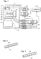
- an electron beam vacuum chamber 4 in which is disposed a conventional electron beam generator 8 of a scanning electron microscope.
- the electron beam generator 8 produces an electron beam 12 which is directed towards a work area 16.
- the direction of the electron beam 12 is under control of a beam scan control unit 20 and may be changed or caused to move along two orthogonal axes (designated the x and y axes) laterally of the beam.
- the beam scan control unit 20 applies analog signals to coils 24 in the electron beam generator 8 to control the direction of the electron beam 12, all in a conventional manner.
- the beam scan control unit 20 might illustratively be a digital-to-analog converter which receives digital signals from a computer 28 identifying the x and y coordinates which the electron beam 12 is to have.
- the computer 28, which controls the overall operation of the system of FIG. 1, could illustratively be a Compaq 386 computer.
- a conventional beam blanking circuit 32 is provided to operate under control of the computer 28 to vary the intensity of electron beam 12. This intensity can be varied from zero (no beam) up to some predetermined upper limit intensity. Such operation is well known.
- a workpiece positioning mechanism 36 for selectively moving and positioning a workpiece 40 which, in the embodiment shown in FIG. 1, is a small cylindrical bar or mandrel.
- the workpiece 40 is held by conventional chuck 44 which, in turn, is rotatably held by a rotary motorized stage 48.
- the rotary stage 48 is mounted on a bracket 52 which, in turn, is mounted on a linear motorized stage 56 which is moveable linearly on a track 60.
- the track 60 is mounted on a base 64 which may be manually moved and positioned in the chamber 4 as desired.
- Both the rotary stage 4 and the linear stage 56 operate under control of the computer 28.
- the rotary stage 48 selectively causes rotation of the chuck 44 which, in turn, causes the workpiece 40 to rotate about an axis which is generally perpendicular to the electron beam 12, as shown.
- the linear stage 56 when it moves linearly on the track 60, carries with it the bracket 52, rotary stage 48, chuck 44 and thus the workpiece 40, in the direction of travel of the linear stage which is a direction parallel to the axis of rotation of the workpiece. In this manner, the workpiece 40 may be selectively moved under the electron beam 12 both rotationally and linearly to cause the electron beam to fall or impinge on different surface areas of the workpiece.
- the electron beam 12 can itself be caused to move orthogonally relative to the location of the workpiece under control of the beam scan control unit 20.
- the rotary motorized stage 48 might illustratively be a 360 degree continuous rotation stage, No. 345,341, manufactured by Klinger, and the linear motorized stage 56 might illustratively be a translational stage, No. MF04 also manufactured by Klinger.
- Control of the operation of the rotary stage 48 and the linear stage 56 is effectuated by a two-axis servo controller 68 and an amplifier 72, again under control of the computer 28.
- the computer 28 supplies signals to the controller 68 in the form of commands for movement of the rotary stage 48 and linear stage 56. These signals are supplied to the amplifier 72 which then supplies rotary command signals to the rotary stage 48 and linear command signals to the linear stage 56 to cause the desired operation of the stages.
- the controller 68 which, in turn, supplies the signals to the computer 28.
- the computer 28 compares the feedback signals with the previously issued command signals to determine if the movement of the stages was in accordance with the command signals, and to make appropriate corrections if needed.
- the two-axis servo controller 68 might illustratively be a Galil DMC-620 controller and the amplifier 72 might illustratively be a Galil ICB-960 amplifier.
- FIG. 2 is a perspective view of a cylindrical bar or mandrel 76 in which parallel lines 80 have been etched in the mandrel using the apparatus of FIG. 1. These lines are etched using an electron beam lithographic process which includes applying an electron beam resist coating to the mandrel, etc. as will be described momentarily.
- the sequence of movement of the mandrel 76 by the chuck 44 would be to position one end of the mandrel in line with the electron beam 12, move the mandrel linearly a distance equal to the length of the line desired be formed in the mandrel, rotate the mandrel by an amount equal to the desired separation of the lines, move the mandrel linearly in the other direction under the electron beam, etc., until the mandrel has been exposed to the electron beam in the desired pattern of the lines.
- FIG. 3 shows another bar or mandrel 84 in which a continuous helical line 88 has been formed thereon.
- the mandrel 84 would be moved by the chuck 44 linearly and rotationally at the same time so that the helical line 88 is exposed to the electron beam.
- degrees of freedom of movement of the workpiece 40 is possible with the apparatus of FIG. 1, clearly other degrees of freedom of movement could also be provided for the workpiece.
- an additional linear degree of freedom of movement could be provided, the direction of which would be generally perpendicular to both the electron beam 12 and the direction of movement of the linear stage 56. This could be done by mounting the track 60 on another linear stage which would be moveable in a direction which was at right angles to the direction and movement of the stage 56.
- the bracket 52 could be mounted on another rotational stage to allow rotation of the bracket and thus the workpiece 40 about an axis generally parallel to the electron beam 12 to thereby provide two rotational degrees of freedom of movement for the workpiece.
- three rotational degrees of freedom of movement could be provided, along with three linear degrees of freedom of movement (although movement toward and away from the electron beam generator 8 in a linear fashion would probably not be too useful), or any combination thereof.
- FIG. 1 utilizes an electron beam 12, it should be understood that the apparatus could be provided for directing a laser beam, ion beam, or an x-ray beam, toward a workpiece in the same manner as that described for the FIG. 1 apparatus.
- An illustrative lithographic process for use with the apparatus of FIG. 1 could include first cleaning the workpiece using solvent such as acetone and two-propanol, or using a hydrogen peroxide cycle. The workpiece is then coated with an adhesion promoter such as HMDS which improves the ability of the electron beam resist to adhere to the workpiece. Electron beam resist would then be applied to the workpiece by simply dipping the workpiece in a solution of the resist. The electron beam resist is then set by soft-baking the workpiece in a convection oven, for example for about 30 minutes at about 80 degrees centigrade. The workpiece is then placed in the chuck 44 and then the electron beam generator 8 and mechanism 36 operated to expose the workpiece to the electron beam 12 to the desired pattern.
- solvent such as acetone and two-propanol
- HMDS an adhesion promoter
- Electron beam resist would then be applied to the workpiece by simply dipping the workpiece in a solution of the resist.
- the electron beam resist is then set by soft-
- the exposed electron beam resist is developed. During development of the exposed pattern, the resist overlying the pattern is washed away (positive lithography) or all other resist except that overlying the pattern is washed away (negative lithography).
- the workpiece is then baked in a convection oven, again for about 30 minutes at 80 degrees centigrade, for example.
- the workpiece is now ready for etching (or deposition) which is carried out by exposing the workpiece to an appropriate etching agent. In positive lithography, the pattern would be etched directly whereas in negative lithography, all except the pattern would be etched into the workpiece. Following the etching step, the remaining electron beam resist is removed and the workpiece is either ready for a next step in the fabrication process or is completed. (Deposition of a desired material on the workpiece, by sputtering, vapor deposition, etc., could be performed in place of etching.)
- Exemplary materials for a workpiece using electron beam lithography include gold, silicon nitride, aluminum, steel and quartz.
- Appropriate etchants for the workpiece materials include phosphoric acid for aluminum, aqua regia for gold, ferric chloride or nitric acid for steel and nitric acid plus hydrofluoric acid for quartz.
Landscapes
- Physics & Mathematics (AREA)
- Engineering & Computer Science (AREA)
- General Physics & Mathematics (AREA)
- Optics & Photonics (AREA)
- Mechanical Engineering (AREA)
- Plasma & Fusion (AREA)
- Robotics (AREA)
- High Energy & Nuclear Physics (AREA)
- Human Computer Interaction (AREA)
- Manufacturing & Machinery (AREA)
- Automation & Control Theory (AREA)
- Electron Beam Exposure (AREA)
- Exposure And Positioning Against Photoresist Photosensitive Materials (AREA)
- Micromachines (AREA)
- Drying Of Semiconductors (AREA)
Applications Claiming Priority (2)
| Application Number | Priority Date | Filing Date | Title |
|---|---|---|---|
| US647659 | 1991-01-28 | ||
| US07/647,659 US5106455A (en) | 1991-01-28 | 1991-01-28 | Method and apparatus for fabrication of micro-structures using non-planar, exposure beam lithography |
Publications (3)
| Publication Number | Publication Date |
|---|---|
| EP0497227A2 true EP0497227A2 (de) | 1992-08-05 |
| EP0497227A3 EP0497227A3 (en) | 1992-09-02 |
| EP0497227B1 EP0497227B1 (de) | 1997-04-16 |
Family
ID=24597809
Family Applications (1)
| Application Number | Title | Priority Date | Filing Date |
|---|---|---|---|
| EP92101182A Expired - Lifetime EP0497227B1 (de) | 1991-01-28 | 1992-01-24 | Verfahren und Gerät zur Herstellung von Mirikostrukturen mittels nicht planarer Lithographie durch Strahlbelichtung |
Country Status (6)
| Country | Link |
|---|---|
| US (1) | US5106455A (de) |
| EP (1) | EP0497227B1 (de) |
| JP (1) | JP3217832B2 (de) |
| AT (1) | ATE151914T1 (de) |
| CA (1) | CA2059345C (de) |
| DE (1) | DE69218983T2 (de) |
Cited By (2)
| Publication number | Priority date | Publication date | Assignee | Title |
|---|---|---|---|---|
| EP0710057A1 (de) * | 1994-10-18 | 1996-05-01 | Ebara Corporation | Energiestrahlquelle und Verfahren zur Schichtbildung mittels einer solchen Quelle |
| EP1408327A3 (de) * | 2002-10-09 | 2004-04-21 | Neocera, Inc. | Eine Öffnung aufweisender Probenkopf zur lokalen Messung der komplexen Dielektrizitätskonstante und Herstellungsverfahren |
Families Citing this family (158)
| Publication number | Priority date | Publication date | Assignee | Title |
|---|---|---|---|---|
| US5273622A (en) * | 1991-01-28 | 1993-12-28 | Sarcos Group | System for continuous fabrication of micro-structures and thin film semiconductor devices on elongate substrates |
| US5270485A (en) * | 1991-01-28 | 1993-12-14 | Sarcos Group | High density, three-dimensional, intercoupled circuit structure |
| US5269882A (en) * | 1991-01-28 | 1993-12-14 | Sarcos Group | Method and apparatus for fabrication of thin film semiconductor devices using non-planar, exposure beam lithography |
| US5481184A (en) * | 1991-12-31 | 1996-01-02 | Sarcos Group | Movement actuator/sensor systems |
| IL105925A (en) * | 1992-06-22 | 1997-01-10 | Martin Marietta Corp | Ablative process for printed circuit board technology |
| CA2089240C (en) * | 1993-02-10 | 1998-07-14 | Stephen C. Jacobsen | Method and apparatus for fabrication of thin film semiconductor devices using non-planar, exposure beam lithography |
| IL106892A0 (en) * | 1993-09-02 | 1993-12-28 | Pierre Badehi | Methods and apparatus for producing integrated circuit devices |
| JP2655474B2 (ja) * | 1993-12-17 | 1997-09-17 | 日本電気株式会社 | 電子線直接描画方法及びその装置 |
| US5833632A (en) | 1995-12-07 | 1998-11-10 | Sarcos, Inc. | Hollow guide wire apparatus catheters |
| US20030069522A1 (en) * | 1995-12-07 | 2003-04-10 | Jacobsen Stephen J. | Slotted medical device |
| US6428489B1 (en) | 1995-12-07 | 2002-08-06 | Precision Vascular Systems, Inc. | Guidewire system |
| CA2192045A1 (en) | 1995-12-07 | 1997-06-08 | Stephen C. Jacobsen | Catheter guide wire apparatus |
| GB9623691D0 (en) * | 1996-11-14 | 1997-01-08 | Simpson Robert W | Machine tools |
| US5955776A (en) * | 1996-12-04 | 1999-09-21 | Ball Semiconductor, Inc. | Spherical shaped semiconductor integrated circuit |
| US6026316A (en) * | 1997-05-15 | 2000-02-15 | Regents Of The University Of Minnesota | Method and apparatus for use with MR imaging |
| US6272370B1 (en) | 1998-08-07 | 2001-08-07 | The Regents Of University Of Minnesota | MR-visible medical device for neurological interventions using nonlinear magnetic stereotaxis and a method imaging |
| US6061587A (en) * | 1997-05-15 | 2000-05-09 | Regents Of The University Of Minnesota | Method and apparatus for use with MR imaging |
| US7048716B1 (en) | 1997-05-15 | 2006-05-23 | Stanford University | MR-compatible devices |
| EP0880078A3 (de) * | 1997-05-23 | 2001-02-14 | Canon Kabushiki Kaisha | Vorrichtung zur Detektion einer Position, Apparat unter Verwendung derselben, Belichtungsapparat, und Verfahren zur Herstellung einer Vorrichtung unter Verwendung desselben |
| US6806477B1 (en) | 1997-05-23 | 2004-10-19 | Canon Kabushiki Kaisha | Position detection device, apparatus using the same, exposure apparatus, and device manufacturing method using the same |
| US5964705A (en) * | 1997-08-22 | 1999-10-12 | Image-Guided Drug Delivery System, Inc. | MR-compatible medical devices |
| US6063200A (en) * | 1998-02-10 | 2000-05-16 | Sarcos L.C. | Three-dimensional micro fabrication device for filamentary substrates |
| US6463317B1 (en) | 1998-05-19 | 2002-10-08 | Regents Of The University Of Minnesota | Device and method for the endovascular treatment of aneurysms |
| US6411362B2 (en) | 1999-01-04 | 2002-06-25 | International Business Machines Corporation | Rotational mask scanning exposure method and apparatus |
| US6529262B1 (en) | 1999-04-14 | 2003-03-04 | Ball Semiconductor, Inc. | System and method for performing lithography on a substrate |
| US6579246B2 (en) | 1999-12-22 | 2003-06-17 | Sarcos, Lc | Coronary guidewire system |
| SE515785C2 (sv) * | 2000-02-23 | 2001-10-08 | Obducat Ab | Anordning för homogen värmning av ett objekt och användning av anordningen |
| US6509955B2 (en) | 2000-05-25 | 2003-01-21 | Ball Semiconductor, Inc. | Lens system for maskless photolithography |
| US6576406B1 (en) | 2000-06-29 | 2003-06-10 | Sarcos Investments Lc | Micro-lithographic method and apparatus using three-dimensional mask |
| US6537738B1 (en) | 2000-08-08 | 2003-03-25 | Ball Semiconductor, Inc. | System and method for making smooth diagonal components with a digital photolithography system |
| US6493867B1 (en) | 2000-08-08 | 2002-12-10 | Ball Semiconductor, Inc. | Digital photolithography system for making smooth diagonal components |
| US6498643B1 (en) | 2000-11-13 | 2002-12-24 | Ball Semiconductor, Inc. | Spherical surface inspection system |
| US6512625B2 (en) | 2000-11-22 | 2003-01-28 | Ball Semiconductor, Inc. | Light modulation device and system |
| US6473237B2 (en) | 2000-11-14 | 2002-10-29 | Ball Semiconductor, Inc. | Point array maskless lithography |
| US6433917B1 (en) | 2000-11-22 | 2002-08-13 | Ball Semiconductor, Inc. | Light modulation device and system |
| ES2274984T3 (es) * | 2001-07-05 | 2007-06-01 | Precision Vascular Systems, Inc. | Dispositivo medico de punta blanda que puede someterse a torsion y metodo para conformarlo. |
| US20030025979A1 (en) * | 2001-07-31 | 2003-02-06 | Ball Semiconductor, Inc. | Surface distortion compensated photolithography |
| US6965387B2 (en) * | 2001-08-03 | 2005-11-15 | Ball Semiconductor, Inc. | Real time data conversion for a digital display |
| WO2003058161A1 (en) * | 2002-01-04 | 2003-07-17 | Parker Hannifin Corporation | Cylinder with optical sensing device and method |
| US7552671B2 (en) * | 2002-01-04 | 2009-06-30 | Parker-Hannifin Corporation | Cylinder with fiber optical position sensing device and method |
| US6870604B2 (en) * | 2002-04-23 | 2005-03-22 | Ball Semiconductor, Inc. | High resolution point array |
| US7164961B2 (en) * | 2002-06-14 | 2007-01-16 | Disco Corporation | Modified photolithography movement system |
| JP4602080B2 (ja) | 2002-07-25 | 2010-12-22 | ボストン サイエンティフィック リミテッド | 人体構造内を進行する医療用具 |
| US7914467B2 (en) * | 2002-07-25 | 2011-03-29 | Boston Scientific Scimed, Inc. | Tubular member having tapered transition for use in a medical device |
| DE10257389A1 (de) | 2002-12-06 | 2004-06-24 | Henkel Kgaa | Flüssiges saures Waschmittel |
| JP4535881B2 (ja) * | 2003-01-09 | 2010-09-01 | 株式会社山武 | 曲面を有する半導体デバイスに露光する装置および方法 |
| US8377035B2 (en) | 2003-01-17 | 2013-02-19 | Boston Scientific Scimed, Inc. | Unbalanced reinforcement members for medical device |
| US20040167437A1 (en) * | 2003-02-26 | 2004-08-26 | Sharrow James S. | Articulating intracorporal medical device |
| US7169118B2 (en) | 2003-02-26 | 2007-01-30 | Scimed Life Systems, Inc. | Elongate medical device with distal cap |
| US7001369B2 (en) | 2003-03-27 | 2006-02-21 | Scimed Life Systems, Inc. | Medical device |
| US7824345B2 (en) * | 2003-12-22 | 2010-11-02 | Boston Scientific Scimed, Inc. | Medical device with push force limiter |
| US20050201698A1 (en) * | 2004-02-12 | 2005-09-15 | Panorama Flat Ltd. | System, method, and computer program product for faceplate for structured waveguide system |
| US20060056792A1 (en) * | 2004-02-12 | 2006-03-16 | Panorama Flat Ltd. | System, method, and computer program product for structured waveguide including intra/inter contacting regions |
| US20050180723A1 (en) * | 2004-02-12 | 2005-08-18 | Panorama Flat Ltd. | Apparatus, method, and computer program product for structured waveguide including holding bounding region |
| US7224854B2 (en) * | 2004-02-12 | 2007-05-29 | Panorama Labs Pty. Ltd. | System, method, and computer program product for structured waveguide including polarizer region |
| US7254287B2 (en) * | 2004-02-12 | 2007-08-07 | Panorama Labs, Pty Ltd. | Apparatus, method, and computer program product for transverse waveguided display system |
| US20050185877A1 (en) * | 2004-02-12 | 2005-08-25 | Panorama Flat Ltd. | Apparatus, Method, and Computer Program Product For Structured Waveguide Switching Matrix |
| US20050201679A1 (en) * | 2004-02-12 | 2005-09-15 | Panorama Flat Ltd. | System, method, and computer program product for structured waveguide including modified output regions |
| US20050201654A1 (en) * | 2004-02-12 | 2005-09-15 | Panorama Flat Ltd. | Apparatus, method, and computer program product for substrated waveguided display system |
| US20050180674A1 (en) * | 2004-02-12 | 2005-08-18 | Panorama Flat Ltd. | Faraday structured waveguide display |
| US20060056794A1 (en) * | 2004-02-12 | 2006-03-16 | Panorama Flat Ltd. | System, method, and computer program product for componentized displays using structured waveguides |
| US20050201705A1 (en) * | 2004-02-12 | 2005-09-15 | Panorama Flat Ltd. | Apparatus, method, and computer program product for structured waveguide including recursion zone |
| US20050180673A1 (en) * | 2004-02-12 | 2005-08-18 | Panorama Flat Ltd. | Faraday structured waveguide |
| US20050180672A1 (en) * | 2004-02-12 | 2005-08-18 | Panorama Flat Ltd. | Apparatus, Method, and Computer Program Product For Multicolor Structured Waveguide |
| US20050180722A1 (en) * | 2004-02-12 | 2005-08-18 | Panorama Flat Ltd. | Apparatus, method, and computer program product for structured waveguide transport |
| US20050180675A1 (en) * | 2004-02-12 | 2005-08-18 | Panorama Flat Limited, A Western Australia Corporation | Apparatus, method, and computer program product for structured waveguide including performance_enhancing bounding region |
| US20060056793A1 (en) * | 2004-02-12 | 2006-03-16 | Panorama Flat Ltd. | System, method, and computer program product for structured waveguide including nonlinear effects |
| US20050201651A1 (en) * | 2004-02-12 | 2005-09-15 | Panorama Flat Ltd. | Apparatus, method, and computer program product for integrated influencer element |
| WO2006044059A2 (en) * | 2004-09-11 | 2006-04-27 | The Board Of Trustees Of The Leland Stanford Junior University | Method and apparatus for modeling the modal properties of optical waveguides |
| US7632242B2 (en) | 2004-12-09 | 2009-12-15 | Boston Scientific Scimed, Inc. | Catheter including a compliant balloon |
| US20060264904A1 (en) * | 2005-05-09 | 2006-11-23 | Kerby Walter L | Medical device |
| CN100390543C (zh) * | 2005-06-08 | 2008-05-28 | 大连理工大学 | 高载微构件动态特性测试装置 |
| US9445784B2 (en) * | 2005-09-22 | 2016-09-20 | Boston Scientific Scimed, Inc | Intravascular ultrasound catheter |
| US7850623B2 (en) | 2005-10-27 | 2010-12-14 | Boston Scientific Scimed, Inc. | Elongate medical device with continuous reinforcement member |
| US8292827B2 (en) * | 2005-12-12 | 2012-10-23 | Boston Scientific Scimed, Inc. | Micromachined medical devices |
| US7999471B2 (en) | 2005-12-12 | 2011-08-16 | Raytheon Company | Multi-cell electronic circuit array and method of manufacturing |
| US8021311B2 (en) * | 2006-08-16 | 2011-09-20 | Boston Scientific Scimed, Inc. | Mechanical honing of metallic tubing for soldering in a medical device construction |
| US20080045908A1 (en) * | 2006-08-16 | 2008-02-21 | Boston Scientific Scimed, Inc. | Medical device including a metallic tube fillet welded to a core member |
| US7833564B2 (en) * | 2006-08-24 | 2010-11-16 | Boston Scientific Scimed, Inc. | Elongate medical device and method of coating the same |
| US7857008B2 (en) * | 2006-08-24 | 2010-12-28 | Boston Scientific Scimed, Inc. | Medical device coating configuration and method for improved lubricity and durability |
| US8419658B2 (en) * | 2006-09-06 | 2013-04-16 | Boston Scientific Scimed, Inc. | Medical device including structure for crossing an occlusion in a vessel |
| KR101419195B1 (ko) * | 2006-09-08 | 2014-07-15 | 가부시키가이샤 니콘 | 마스크, 노광 장치 및 디바이스 제조 방법 |
| JP2010503484A (ja) * | 2006-09-13 | 2010-02-04 | ボストン サイエンティフィック リミテッド | 横断ガイドワイヤ |
| US8556914B2 (en) | 2006-12-15 | 2013-10-15 | Boston Scientific Scimed, Inc. | Medical device including structure for crossing an occlusion in a vessel |
| US20080262474A1 (en) * | 2007-04-20 | 2008-10-23 | Boston Scientific Scimed, Inc. | Medical device |
| US8409114B2 (en) * | 2007-08-02 | 2013-04-02 | Boston Scientific Scimed, Inc. | Composite elongate medical device including distal tubular member |
| US20090036832A1 (en) * | 2007-08-03 | 2009-02-05 | Boston Scientific Scimed, Inc. | Guidewires and methods for manufacturing guidewires |
| US8105246B2 (en) * | 2007-08-03 | 2012-01-31 | Boston Scientific Scimed, Inc. | Elongate medical device having enhanced torque and methods thereof |
| US20090043228A1 (en) * | 2007-08-06 | 2009-02-12 | Boston Scientific Scimed, Inc. | Laser shock peening of medical devices |
| US8821477B2 (en) * | 2007-08-06 | 2014-09-02 | Boston Scientific Scimed, Inc. | Alternative micromachined structures |
| US9808595B2 (en) * | 2007-08-07 | 2017-11-07 | Boston Scientific Scimed, Inc | Microfabricated catheter with improved bonding structure |
| US20090118704A1 (en) * | 2007-11-02 | 2009-05-07 | Boston Scientific Scimed, Inc. | Interconnected ribbon coils, medical devices including an interconnected ribbon coil, and methods for manufacturing an interconnected ribbon coil |
| US7841994B2 (en) | 2007-11-02 | 2010-11-30 | Boston Scientific Scimed, Inc. | Medical device for crossing an occlusion in a vessel |
| US20090118675A1 (en) * | 2007-11-02 | 2009-05-07 | Boston Scientific Scimed, Inc. | Elongate medical device with a shapeable tip |
| US20090157047A1 (en) * | 2007-12-13 | 2009-06-18 | Boston Scientific Scimed, Inc. | Medical device coatings and methods of forming such coatings |
| US8460213B2 (en) | 2008-01-03 | 2013-06-11 | Boston Scientific Scimed, Inc. | Cut tubular members for a medical device and methods for making and using the same |
| US8376961B2 (en) | 2008-04-07 | 2013-02-19 | Boston Scientific Scimed, Inc. | Micromachined composite guidewire structure with anisotropic bending properties |
| US20090264907A1 (en) * | 2008-04-18 | 2009-10-22 | Boston Scientific Scimed, Inc. | Medical device for crossing an occluded blood vessel |
| US9182252B2 (en) | 2008-05-16 | 2015-11-10 | Parker Hannifin Corporation | Probe for determining an absolute position of a rod of a cylinder |
| US20100048758A1 (en) * | 2008-08-22 | 2010-02-25 | Boston Scientific Scimed, Inc. | Lubricious coating composition for devices |
| US8535243B2 (en) * | 2008-09-10 | 2013-09-17 | Boston Scientific Scimed, Inc. | Medical devices and tapered tubular members for use in medical devices |
| US20100063479A1 (en) * | 2008-09-10 | 2010-03-11 | Boston Scientific Scimed, Inc. | Small profile, tubular component design and method of manufacture |
| US20100069882A1 (en) * | 2008-09-18 | 2010-03-18 | Boston Scientific Scimed, Inc. | Medical device with preferential bending |
| US8795254B2 (en) * | 2008-12-10 | 2014-08-05 | Boston Scientific Scimed, Inc. | Medical devices with a slotted tubular member having improved stress distribution |
| US8137293B2 (en) | 2009-11-17 | 2012-03-20 | Boston Scientific Scimed, Inc. | Guidewires including a porous nickel-titanium alloy |
| JP2013523282A (ja) | 2010-03-31 | 2013-06-17 | ボストン サイエンティフィック サイムド,インコーポレイテッド | 曲げ剛性プロファイルを有するガイドワイヤ |
| CN103328033B (zh) | 2010-11-09 | 2016-05-18 | 奥普森斯公司 | 具有内部压力传感器的导丝 |
| EP2670470B1 (de) | 2011-02-04 | 2019-04-24 | Boston Scientific Scimed, Inc. | Führungsdrähte |
| WO2012109468A1 (en) | 2011-02-09 | 2012-08-16 | Boston Scientific Scimed, Inc. | Balloon catheter |
| WO2012122183A1 (en) | 2011-03-07 | 2012-09-13 | Stryker Corporation | Balloon catheter and support shaft for same |
| US9072874B2 (en) | 2011-05-13 | 2015-07-07 | Boston Scientific Scimed, Inc. | Medical devices with a heat transfer region and a heat sink region and methods for manufacturing medical devices |
| EP2765942B1 (de) | 2011-10-10 | 2016-02-24 | Boston Scientific Scimed, Inc. | Medizinische vorrichtungen mit ablationselektroden |
| EP2768563B1 (de) | 2011-10-18 | 2016-11-09 | Boston Scientific Scimed, Inc. | Biegbare medizinische vorrichtungen |
| US8911398B2 (en) | 2011-11-04 | 2014-12-16 | Boston Scientific Scimed, Inc. | Catheter including a bare metal hypotube |
| WO2013070758A2 (en) | 2011-11-09 | 2013-05-16 | Boston Scientific Scimed, Inc. | Guide extension catheter |
| CN104159535A (zh) | 2012-01-17 | 2014-11-19 | 波士顿科学西美德公司 | 肾神经调节装置以及用于制造和使用该装置的方法 |
| US9358370B2 (en) * | 2012-03-12 | 2016-06-07 | Medtronic Vascular, Inc. | Guidewire with integral radiopaque markers |
| WO2014005095A1 (en) | 2012-06-29 | 2014-01-03 | Boston Scientific Scimed, Inc. | Pressure sensing guidewire |
| US20140025044A1 (en) | 2012-07-19 | 2014-01-23 | Boston Scientific Scimed, Inc. | Torqueable catheter hub and related methods of use |
| US9486611B2 (en) | 2012-08-17 | 2016-11-08 | Boston Scientific Scimed, Inc. | Guide extension catheter |
| CN105142506A (zh) | 2012-08-27 | 2015-12-09 | 波士顿科学国际有限公司 | 压力感测医疗器械及医疗器械系统 |
| JP6086984B2 (ja) | 2012-09-17 | 2017-03-01 | ボストン サイエンティフィック サイムド,インコーポレイテッドBoston Scientific Scimed,Inc. | 圧力検知ガイドワイヤ |
| WO2014052648A1 (en) | 2012-09-26 | 2014-04-03 | Boston Scientific Scimed, Inc. | Renal nerve modulation devices |
| US20140088585A1 (en) | 2012-09-26 | 2014-03-27 | Boston Scientific Scimed, Inc. | Catheter having rib and spine structure supporting multiple electrodes for renal nerve ablation |
| US20140094787A1 (en) | 2012-09-28 | 2014-04-03 | Boston Scientific Scimed, Inc. | Flexible renal nerve modulation device |
| WO2014066104A1 (en) | 2012-10-25 | 2014-05-01 | Boston Scientific Scimed, Inc. | Dual function medical devices |
| EP2968854B1 (de) | 2013-03-15 | 2019-04-24 | Boston Scientific Scimed, Inc. | Druckmessungsführungsdraht |
| CN105682544B (zh) | 2013-05-22 | 2019-09-24 | 波士顿科学国际有限公司 | 包括光连接器光缆的压力检测导丝系统 |
| CN105578952B (zh) | 2013-07-26 | 2019-03-19 | 波士顿科学国际有限公司 | 最小化由应力引起的压力偏载的ffr传感头设计 |
| WO2015023789A1 (en) | 2013-08-14 | 2015-02-19 | Boston Scientific Scimed, Inc. | Medical device systems including an optical fiber with a tapered core |
| WO2015057518A1 (en) | 2013-10-14 | 2015-04-23 | Boston Scientific Scimed, Inc. | Pressure sensing guidewire and methods for calculating fractional flow reserve |
| WO2015142623A1 (en) | 2014-03-18 | 2015-09-24 | Boston Scientific Scimed, Inc. | Pressure sensing guidewires |
| US9901706B2 (en) | 2014-04-11 | 2018-02-27 | Boston Scientific Scimed, Inc. | Catheters and catheter shafts |
| CN106456277B (zh) | 2014-04-17 | 2020-03-27 | 波士顿科学国际有限公司 | 自清洗光连接器 |
| WO2015187385A1 (en) | 2014-06-04 | 2015-12-10 | Boston Scientific Scimed, Inc. | Pressure sensing guidewire systems with reduced pressure offsets |
| WO2016011127A2 (en) | 2014-07-18 | 2016-01-21 | Stryker Corporation | Coated tubular support members and methods of manufacturing same |
| CN106714675B (zh) | 2014-08-01 | 2020-03-20 | 波士顿科学国际有限公司 | 压力传感导丝 |
| WO2016073597A1 (en) | 2014-11-06 | 2016-05-12 | Boston Scientific Scimed, Inc. | Tracheal stent |
| WO2016090272A1 (en) | 2014-12-05 | 2016-06-09 | Boston Scientific Scimed, Inc. | Pressure sensing guidewires |
| WO2017004194A1 (en) | 2015-06-30 | 2017-01-05 | Boston Scientific Scimed, Inc. | Medical device having outer polymeric member including one or more cuts |
| WO2017039979A1 (en) | 2015-08-28 | 2017-03-09 | Boston Scientific Scimed, Inc. | Pressure sensing guidewires |
| CN117653061A (zh) | 2015-09-04 | 2024-03-08 | 波士顿科学国际有限公司 | 压力传感导丝 |
| US11351048B2 (en) | 2015-11-16 | 2022-06-07 | Boston Scientific Scimed, Inc. | Stent delivery systems with a reinforced deployment sheath |
| EP3402562B1 (de) | 2016-01-15 | 2022-12-21 | Boston Scientific Scimed, Inc. | Geschlitztes rohr mit planarer lenkung |
| WO2017147165A1 (en) | 2016-02-23 | 2017-08-31 | Boston Scientific Scimed, Inc. | Pressure sensing guidewire systems including an optical connector cable |
| US10537709B2 (en) | 2016-10-18 | 2020-01-21 | Boston Scientific Scimed, Inc. | Guide extension catheter |
| CN116327157B (zh) | 2017-08-03 | 2025-09-30 | 波士顿科学国际有限公司 | 血流储备分数的评估方法 |
| WO2019118792A1 (en) | 2017-12-15 | 2019-06-20 | Boston Scientific Scimed, Inc. | Medical device for accessing and/or treating the neural vasculature |
| US11311196B2 (en) | 2018-02-23 | 2022-04-26 | Boston Scientific Scimed, Inc. | Methods for assessing a vessel with sequential physiological measurements |
| WO2019183432A1 (en) | 2018-03-23 | 2019-09-26 | Boston Scientific Scimed, Inc. | Medical device with pressure sensor |
| CN112292074B (zh) | 2018-04-06 | 2024-05-10 | 波士顿科学国际有限公司 | 具有压力传感器的医疗设备 |
| CN119564167A (zh) | 2018-04-18 | 2025-03-07 | 波士顿科学国际有限公司 | 用连续生理测量值评估脉管的系统 |
| WO2022031706A1 (en) | 2020-08-05 | 2022-02-10 | Boston Scientific Scimed, Inc. | Devices for treating a stricture along the biliary and/or pancreatic tract |
| US12087000B2 (en) | 2021-03-05 | 2024-09-10 | Boston Scientific Scimed, Inc. | Systems and methods for vascular image co-registration |
| US20230166079A1 (en) | 2021-11-29 | 2023-06-01 | Boston Scientific Medical Device Limited | Steerable elongate medical device |
| US20230277815A1 (en) | 2022-03-07 | 2023-09-07 | Boston Scientific Scimed Inc. | Adaptive Coil Guidewire |
| EP4511098A2 (de) | 2022-05-18 | 2025-02-26 | Boston Scientific Medical Device Limited | Medizinische vorrichtung mit lenkbarer spitze |
| US20250331907A1 (en) | 2024-04-25 | 2025-10-30 | Boston Scientific Medical Device Limited | Actively steerable sphincterotome |
Family Cites Families (8)
| Publication number | Priority date | Publication date | Assignee | Title |
|---|---|---|---|---|
| US3770936A (en) * | 1968-11-29 | 1973-11-06 | Westinghouse Electric Corp | Apparatus for sculpturing an indicia or decorative design in the surface of an article with a beam of corpuscular energy |
| CA1084322A (en) * | 1976-10-05 | 1980-08-26 | Murray M. Schiffman | Photographically transferring a design to a flat or arcuate surface |
| US4233123A (en) * | 1978-12-18 | 1980-11-11 | General Motors Corporation | Method for making an air cooled combustor |
| US4788431A (en) * | 1987-04-10 | 1988-11-29 | The Perkin-Elmer Corporation | Specimen distance measuring system |
| GB8719412D0 (en) * | 1987-08-17 | 1987-09-23 | Zed Instr Ltd | Preparing screen |
| JPH0651913B2 (ja) * | 1988-04-22 | 1994-07-06 | 川崎製鉄株式会社 | 圧延用ロールの表面加工方法及びその装置並びに該方法により製造されるプレス加工用金属薄板とその製造方法 |
| FR2639567B1 (fr) * | 1988-11-25 | 1991-01-25 | France Etat | Machine a microfaisceau laser d'intervention sur des objets a couche mince, en particulier pour la gravure ou le depot de matiere par voie chimique en presence d'un gaz reactif |
| US4940508A (en) * | 1989-06-26 | 1990-07-10 | Digital Equipment Corporation | Apparatus and method for forming die sites in a high density electrical interconnecting structure |
-
1991
- 1991-01-28 US US07/647,659 patent/US5106455A/en not_active Expired - Lifetime
-
1992
- 1992-01-14 CA CA002059345A patent/CA2059345C/en not_active Expired - Fee Related
- 1992-01-24 EP EP92101182A patent/EP0497227B1/de not_active Expired - Lifetime
- 1992-01-24 AT AT92101182T patent/ATE151914T1/de not_active IP Right Cessation
- 1992-01-24 DE DE69218983T patent/DE69218983T2/de not_active Expired - Fee Related
- 1992-01-28 JP JP01296892A patent/JP3217832B2/ja not_active Expired - Lifetime
Cited By (4)
| Publication number | Priority date | Publication date | Assignee | Title |
|---|---|---|---|---|
| EP0710057A1 (de) * | 1994-10-18 | 1996-05-01 | Ebara Corporation | Energiestrahlquelle und Verfahren zur Schichtbildung mittels einer solchen Quelle |
| US5989779A (en) * | 1994-10-18 | 1999-11-23 | Ebara Corporation | Fabrication method employing and energy beam source |
| US5998097A (en) * | 1994-10-18 | 1999-12-07 | Ebara Corporation | Fabrication method employing energy beam source |
| EP1408327A3 (de) * | 2002-10-09 | 2004-04-21 | Neocera, Inc. | Eine Öffnung aufweisender Probenkopf zur lokalen Messung der komplexen Dielektrizitätskonstante und Herstellungsverfahren |
Also Published As
| Publication number | Publication date |
|---|---|
| EP0497227A3 (en) | 1992-09-02 |
| CA2059345A1 (en) | 1992-07-29 |
| DE69218983D1 (de) | 1997-05-22 |
| JP3217832B2 (ja) | 2001-10-15 |
| JPH06134586A (ja) | 1994-05-17 |
| ATE151914T1 (de) | 1997-05-15 |
| DE69218983T2 (de) | 1997-07-24 |
| US5106455A (en) | 1992-04-21 |
| EP0497227B1 (de) | 1997-04-16 |
| CA2059345C (en) | 1998-12-01 |
Similar Documents
| Publication | Publication Date | Title |
|---|---|---|
| US5106455A (en) | Method and apparatus for fabrication of micro-structures using non-planar, exposure beam lithography | |
| US5269882A (en) | Method and apparatus for fabrication of thin film semiconductor devices using non-planar, exposure beam lithography | |
| EP0574861B1 (de) | System zur Fliessfertigung von Mikro-Struktur und dünne Schicht-Halbleiter-Einrichtung auf verlängertem Substrat | |
| JP2932650B2 (ja) | 微細構造物の製造方法 | |
| US5375064A (en) | Method and apparatus for moving a material removal tool with low tool accelerations | |
| US6576406B1 (en) | Micro-lithographic method and apparatus using three-dimensional mask | |
| EP0238690A1 (de) | Verfahren zur Herstellung von Seitenstrukturen | |
| Vasile et al. | Focused ion beam technology applied to microstructure fabrication | |
| US5708267A (en) | Processing method using fast atom beam | |
| EP0613170B1 (de) | Verfahren und Gerät zur Herstellung von Dünnfilm-Halbleitervorrichtungen mittels nicht-planarer Strahlbelichtungslithographie | |
| JPH08206866A (ja) | エネルギービーム加工法及びエネルギービーム加工装置 | |
| JPH08318387A (ja) | エネルギービームによる処理方法および処理装置 | |
| JPH076945A (ja) | 非平面露光ビームリトグラフィーを用いて薄膜半導体デバイスを作製する方法及び装置 | |
| JP2668537B2 (ja) | レジスト処理装置及びレジスト処理方法 | |
| JP3360282B2 (ja) | 微細構造体の製造方法 | |
| JPS6351641A (ja) | 単結晶または多結晶Si膜の微細パタ−ン形成方法 | |
| JPS59104287A (ja) | レ−ザ加工法 | |
| JP3804293B2 (ja) | 微小構造体の製造方法および製造装置 | |
| JP2001201627A (ja) | 回折素子の製造方法 | |
| JP3227089B2 (ja) | 位置決めステージ装置およびこれを用いた露光装置ならびにディバイス製造方法 | |
| Ghantasala et al. | Excimer laser micromachining of structures using SU-8 | |
| JP2697035B2 (ja) | フォトマスクの製造方法 | |
| JP3440516B2 (ja) | 移動テーブルの位置制御方法とその制御装置 | |
| JP2558128B2 (ja) | 金属配線の形成方法 | |
| JPH0395917A (ja) | 露光装置及び露光方法 |
Legal Events
| Date | Code | Title | Description |
|---|---|---|---|
| PUAI | Public reference made under article 153(3) epc to a published international application that has entered the european phase |
Free format text: ORIGINAL CODE: 0009012 |
|
| PUAL | Search report despatched |
Free format text: ORIGINAL CODE: 0009013 |
|
| AK | Designated contracting states |
Kind code of ref document: A2 Designated state(s): AT BE CH DE DK ES FR GB GR IT LI NL SE |
|
| AK | Designated contracting states |
Kind code of ref document: A3 Designated state(s): AT BE CH DE DK ES FR GB GR IT LI NL SE |
|
| 17P | Request for examination filed |
Effective date: 19930125 |
|
| 17Q | First examination report despatched |
Effective date: 19950512 |
|
| GRAG | Despatch of communication of intention to grant |
Free format text: ORIGINAL CODE: EPIDOS AGRA |
|
| GRAH | Despatch of communication of intention to grant a patent |
Free format text: ORIGINAL CODE: EPIDOS IGRA |
|
| GRAH | Despatch of communication of intention to grant a patent |
Free format text: ORIGINAL CODE: EPIDOS IGRA |
|
| GRAA | (expected) grant |
Free format text: ORIGINAL CODE: 0009210 |
|
| AK | Designated contracting states |
Kind code of ref document: B1 Designated state(s): AT BE CH DE DK ES FR GB GR IT LI NL SE |
|
| PG25 | Lapsed in a contracting state [announced via postgrant information from national office to epo] |
Ref country code: AT Effective date: 19970416 Ref country code: ES Free format text: THE PATENT HAS BEEN ANNULLED BY A DECISION OF A NATIONAL AUTHORITY Effective date: 19970416 Ref country code: DK Effective date: 19970416 Ref country code: GR Free format text: LAPSE BECAUSE OF FAILURE TO SUBMIT A TRANSLATION OF THE DESCRIPTION OR TO PAY THE FEE WITHIN THE PRESCRIBED TIME-LIMIT Effective date: 19970416 Ref country code: NL Effective date: 19970416 Ref country code: IT Free format text: LAPSE BECAUSE OF FAILURE TO SUBMIT A TRANSLATION OF THE DESCRIPTION OR TO PAY THE FEE WITHIN THE PRE;WARNING: LAPSES OF ITALIAN PATENTS WITH EFFECTIVE DATE BEFORE 2007 MAY HAVE OCCURRED AT ANY TIME BEFORE 2007. THE CORRECT EFFECTIVE DATE MAY BE DIFFERENT FROM THE ONE RECORDED.SCRIBED TIME-LIMIT Effective date: 19970416 |
|
| REF | Corresponds to: |
Ref document number: 151914 Country of ref document: AT Date of ref document: 19970515 Kind code of ref document: T |
|
| ET | Fr: translation filed | ||
| REG | Reference to a national code |
Ref country code: CH Ref legal event code: EP Ref country code: CH Ref legal event code: NV Representative=s name: PATENTANWALTSBUERO JEAN HUNZIKER |
|
| REF | Corresponds to: |
Ref document number: 69218983 Country of ref document: DE Date of ref document: 19970522 |
|
| PG25 | Lapsed in a contracting state [announced via postgrant information from national office to epo] |
Ref country code: SE Effective date: 19970716 |
|
| NLV1 | Nl: lapsed or annulled due to failure to fulfill the requirements of art. 29p and 29m of the patents act | ||
| PLBE | No opposition filed within time limit |
Free format text: ORIGINAL CODE: 0009261 |
|
| STAA | Information on the status of an ep patent application or granted ep patent |
Free format text: STATUS: NO OPPOSITION FILED WITHIN TIME LIMIT |
|
| 26N | No opposition filed | ||
| PGFP | Annual fee paid to national office [announced via postgrant information from national office to epo] |
Ref country code: BE Payment date: 20010201 Year of fee payment: 10 |
|
| PGFP | Annual fee paid to national office [announced via postgrant information from national office to epo] |
Ref country code: GB Payment date: 20010202 Year of fee payment: 10 |
|
| REG | Reference to a national code |
Ref country code: GB Ref legal event code: IF02 |
|
| PG25 | Lapsed in a contracting state [announced via postgrant information from national office to epo] |
Ref country code: GB Free format text: LAPSE BECAUSE OF NON-PAYMENT OF DUE FEES Effective date: 20020124 |
|
| PG25 | Lapsed in a contracting state [announced via postgrant information from national office to epo] |
Ref country code: BE Free format text: LAPSE BECAUSE OF NON-PAYMENT OF DUE FEES Effective date: 20020131 |
|
| BERE | Be: lapsed |
Owner name: SARCOS GROUP Effective date: 20020131 |
|
| GBPC | Gb: european patent ceased through non-payment of renewal fee |
Effective date: 20020124 |
|
| PGFP | Annual fee paid to national office [announced via postgrant information from national office to epo] |
Ref country code: CH Payment date: 20070110 Year of fee payment: 16 |
|
| PGFP | Annual fee paid to national office [announced via postgrant information from national office to epo] |
Ref country code: DE Payment date: 20070131 Year of fee payment: 16 |
|
| PGFP | Annual fee paid to national office [announced via postgrant information from national office to epo] |
Ref country code: FR Payment date: 20070103 Year of fee payment: 16 |
|
| REG | Reference to a national code |
Ref country code: CH Ref legal event code: PL |
|
| PG25 | Lapsed in a contracting state [announced via postgrant information from national office to epo] |
Ref country code: DE Free format text: LAPSE BECAUSE OF NON-PAYMENT OF DUE FEES Effective date: 20080801 Ref country code: CH Free format text: LAPSE BECAUSE OF NON-PAYMENT OF DUE FEES Effective date: 20080131 Ref country code: LI Free format text: LAPSE BECAUSE OF NON-PAYMENT OF DUE FEES Effective date: 20080131 |
|
| REG | Reference to a national code |
Ref country code: FR Ref legal event code: ST Effective date: 20081029 |
|
| PG25 | Lapsed in a contracting state [announced via postgrant information from national office to epo] |
Ref country code: FR Free format text: LAPSE BECAUSE OF NON-PAYMENT OF DUE FEES Effective date: 20080131 |