EP0497290A2 - Schaltungshalbleiterbauelement und Verfahren zur Herstellung desselben - Google Patents
Schaltungshalbleiterbauelement und Verfahren zur Herstellung desselben Download PDFInfo
- Publication number
- EP0497290A2 EP0497290A2 EP92101387A EP92101387A EP0497290A2 EP 0497290 A2 EP0497290 A2 EP 0497290A2 EP 92101387 A EP92101387 A EP 92101387A EP 92101387 A EP92101387 A EP 92101387A EP 0497290 A2 EP0497290 A2 EP 0497290A2
- Authority
- EP
- European Patent Office
- Prior art keywords
- charged particles
- forming
- layer
- semiconductor device
- epitaxial layer
- Prior art date
- Legal status (The legal status is an assumption and is not a legal conclusion. Google has not performed a legal analysis and makes no representation as to the accuracy of the status listed.)
- Withdrawn
Links
Images

Classifications
-
- H—ELECTRICITY
- H10—SEMICONDUCTOR DEVICES; ELECTRIC SOLID-STATE DEVICES NOT OTHERWISE PROVIDED FOR
- H10D—INORGANIC ELECTRIC SEMICONDUCTOR DEVICES
- H10D8/00—Diodes
-
- H—ELECTRICITY
- H10—SEMICONDUCTOR DEVICES; ELECTRIC SOLID-STATE DEVICES NOT OTHERWISE PROVIDED FOR
- H10P—GENERIC PROCESSES OR APPARATUS FOR THE MANUFACTURE OR TREATMENT OF DEVICES COVERED BY CLASS H10
- H10P34/00—Irradiation with electromagnetic or particle radiation of wafers, substrates or parts of devices
- H10P34/40—Irradiation with electromagnetic or particle radiation of wafers, substrates or parts of devices with high-energy radiation
-
- H—ELECTRICITY
- H10—SEMICONDUCTOR DEVICES; ELECTRIC SOLID-STATE DEVICES NOT OTHERWISE PROVIDED FOR
- H10D—INORGANIC ELECTRIC SEMICONDUCTOR DEVICES
- H10D62/00—Semiconductor bodies, or regions thereof, of devices having potential barriers
- H10D62/50—Physical imperfections
- H10D62/53—Physical imperfections the imperfections being within the semiconductor body
-
- H—ELECTRICITY
- H10—SEMICONDUCTOR DEVICES; ELECTRIC SOLID-STATE DEVICES NOT OTHERWISE PROVIDED FOR
- H10D—INORGANIC ELECTRIC SEMICONDUCTOR DEVICES
- H10D8/00—Diodes
- H10D8/01—Manufacture or treatment
-
- H—ELECTRICITY
- H10—SEMICONDUCTOR DEVICES; ELECTRIC SOLID-STATE DEVICES NOT OTHERWISE PROVIDED FOR
- H10P—GENERIC PROCESSES OR APPARATUS FOR THE MANUFACTURE OR TREATMENT OF DEVICES COVERED BY CLASS H10
- H10P14/00—Formation of materials, e.g. in the shape of layers or pillars
- H10P14/60—Formation of materials, e.g. in the shape of layers or pillars of insulating materials
- H10P14/63—Formation of materials, e.g. in the shape of layers or pillars of insulating materials characterised by the formation processes
- H10P14/6326—Deposition processes
- H10P14/6349—Deposition of epitaxial materials
-
- H—ELECTRICITY
- H10—SEMICONDUCTOR DEVICES; ELECTRIC SOLID-STATE DEVICES NOT OTHERWISE PROVIDED FOR
- H10P—GENERIC PROCESSES OR APPARATUS FOR THE MANUFACTURE OR TREATMENT OF DEVICES COVERED BY CLASS H10
- H10P32/00—Diffusion of dopants within, into or out of wafers, substrates or parts of devices
-
- H—ELECTRICITY
- H10—SEMICONDUCTOR DEVICES; ELECTRIC SOLID-STATE DEVICES NOT OTHERWISE PROVIDED FOR
- H10P—GENERIC PROCESSES OR APPARATUS FOR THE MANUFACTURE OR TREATMENT OF DEVICES COVERED BY CLASS H10
- H10P50/00—Etching of wafers, substrates or parts of devices
- H10P50/20—Dry etching; Plasma etching; Reactive-ion etching
Definitions
- the present invention relates to a method of manufacturing a switching semiconductor device, and more particularly to a method of manufacturing a switching semiconductor device, suitable for use in manufacturing high speed switching elements.
- Fig. 1 is a cross sectional view of a general high speed switching diode.
- this high speed switching diode includes a semiconductor substrate 1 placed on a bottom electrode 7.
- First and second epitaxial layers 2 and 3 are formed on this substrate 1.
- the first epitaxial layer 2 has a specific resistance of 1 ⁇ cm and a thickness of 10 ⁇ m
- the second epitaxial layer has a specific resistance of 50 ⁇ cm and a thickness of 70 ⁇ m.
- a semiconductor layer 4 of an opposite conductivity type is grown in the second epitaxial layer 3.
- a field protective film 5 having an opening 5a is formed on the semiconductor layer 4, and an electrode 6 is connected to the layer 4.
- an electron beam is radiated at 10 Mev and at a dose of 5 x 10¹³/cm2, and platinum is diffused.
- Switching semiconductor devices have been manufactured by the method described above, which results in some problems of many manufacturing processes and a relatively low switching speed.
- High speed switching diodes are required to have a high surge voltage tolerance and a high switching speed.
- three manufacturing processes are required, including a process of forming the first epitaxial layer, a process of radiating an electron beam, and a process of diffusing platinum.
- electron beam radiation and platinum diffusion are required in order to control the life time of carriers.
- radiation of an electron beam to a semiconductor device may generate defects in the semiconductor device and raise an on-voltage. Therefore, a dose of electrons is limited, disabling to set a switching speed too high.
- Charged particles are radiated to the epitaxial growth layer on the semiconductor substrate to form the high carrier concentration region between the Substrate and the epitaxial layer.
- the charged particles radiated by this process shorten the carrier life time at the proton pass region, and increase the carrier concentration at the proton stop region. Therefore, a manufactured switching semiconductor device has a considerably improved switching speed.
- only one process charged particles radiation process
- epitaxial growth process, electron beam radiation process, and platinum diffusion process is required instead of conventional three processes (epitaxial growth process, electron beam radiation process, and platinum diffusion process).
- Fig. 1 is a cross sectional view of a switching semiconductor device manufactured by a conventional method.
- Fig. 2 is a schematic diagram showing a method of manufacturing a Switching semiconductor device according to an embodiment of the present invention.
- Fig. 3 is a cross sectional view of a semiconductor device manufactured by the method of the present invention.
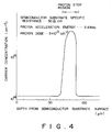
- Fig. 4 is a graph showing a carrier concentration relative to a depth of a semiconductor substrate radiated with protons.
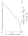
- Fig. 5 is a graph showing a proton dose relative to a carrier concentration.
- Fig. 2 is a schematic diagram showing a method of manufacturing a semiconductor device according to the embodiment of the present invention.
- a semiconductor substrate 1 is placed on a bottom electrode 7.
- an epitaxial growth layer 8 having a specific resistance of 50 ⁇ cm and a thickness of 80 ⁇ m.
- a semiconductor layer 4 of an opposite conduction type is grown.
- a field protective film 5 having an opening 5a is formed.
- an electrode 6 is formed in contact with the layer 4 via the opening 5a. Protons as charged particles are radiated at an acceleration energy of 2.6 MeV and at a dose of 5 x 10¹³/cm2. In this manner, a semiconductor device is manufactured.
- proton radiation at an acceleration energy of 2.6 MeV provides a radiation range of about 80 ⁇ m within silicon. Accordingly, protons stop at the boundary region between the semiconductor substrate 1 and epitaxial growth layer 8. As seen from the cross section shown in Fig. 3, the carrier concentration increases at the proton stop region, forming a high carrier concentration region 9.
- a thermal process is carried out in an N2 atmosphere at 350°C and for 60 minutes.
- the carrier concentration considerably increases over the range in excess of a proton dose of 1 x 10¹²/cm2, as shown in Fig. 5.
- the carrier concentration at the proton stop region is 4.8 x 10¹⁵/cm ⁇ 3 which is substantially the same as the carrier concentration of 7 x 10¹⁵/cm ⁇ 3 of the conventional first epitaxial growth layer 2. Therefore, even the device structure shown in Fig. 3 can have a sufficient surge voltage tolerance. Defects within the proton pass region are generated at the region deeper than that generated by electron beam radiation, and the detect level density generated by proton radiation is greater than electron beam radiation by one digit or more. As a result, the carrier life time is shortened at the proton pass region, allowing to manufacture a high speed switching semiconductor device.
- a device manufactured by the present invention method has a higher switching speed and smaller on-voltage, than those of a device manufactured by the conventional method.
- Table 1 Switching Speed On-voltage Device of Conventional Method 112 nsec 2.5 v Device of Invention Method 55 nsec 2 V
- the conventional method requires an epitaxial growth process, electron beam radiation process, and platinum diffusion process.
- the embodiment method replaces the three processes by only one process of proton radiation. As a result, the number of manufacturing steps and the number of manufacture days can be greatly reduced.
- charged particles heavy hydrogen ions or helium ions may be used.
Landscapes
- Thyristors (AREA)
- Bipolar Transistors (AREA)
- Recrystallisation Techniques (AREA)
Applications Claiming Priority (2)
| Application Number | Priority Date | Filing Date | Title |
|---|---|---|---|
| JP8725/91 | 1991-01-28 | ||
| JP3008725A JPH04252078A (ja) | 1991-01-28 | 1991-01-28 | スイッチング半導体装置の製造方法 |
Publications (2)
| Publication Number | Publication Date |
|---|---|
| EP0497290A2 true EP0497290A2 (de) | 1992-08-05 |
| EP0497290A3 EP0497290A3 (en) | 1995-11-29 |
Family
ID=11700932
Family Applications (1)
| Application Number | Title | Priority Date | Filing Date |
|---|---|---|---|
| EP92101387A Withdrawn EP0497290A3 (en) | 1991-01-28 | 1992-01-28 | Switching semiconductor device and method of manufacturing the same |
Country Status (3)
| Country | Link |
|---|---|
| EP (1) | EP0497290A3 (de) |
| JP (1) | JPH04252078A (de) |
| KR (1) | KR950001170B1 (de) |
Cited By (3)
| Publication number | Priority date | Publication date | Assignee | Title |
|---|---|---|---|---|
| WO2004030103A1 (de) * | 2002-09-20 | 2004-04-08 | Infineon Technologies Ag | Verfahren zur herstellung einer vergrabenen stoppzone in einem halbleiterbauelement und halbleiterbauelement mit einer vergrabenen stoppzone |
| US7799662B2 (en) | 2005-11-14 | 2010-09-21 | Fuji Electric Systems Co., Ltd. | Power semiconductor device with soft switching characteristic and manufacturing method for same |
| CN109300994A (zh) * | 2018-09-27 | 2019-02-01 | 上海长园维安微电子有限公司 | 一种伪负阻型低残压tvs器件及其制备方法 |
Families Citing this family (2)
| Publication number | Priority date | Publication date | Assignee | Title |
|---|---|---|---|---|
| WO2000016408A1 (en) * | 1998-09-10 | 2000-03-23 | Mitsubishi Denki Kabushiki Kaisha | Semiconductor device and its manufacturing method |
| JP5374883B2 (ja) | 2008-02-08 | 2013-12-25 | 富士電機株式会社 | 半導体装置およびその製造方法 |
Family Cites Families (6)
| Publication number | Priority date | Publication date | Assignee | Title |
|---|---|---|---|---|
| JPS518869A (ja) * | 1974-07-09 | 1976-01-24 | Mitsubishi Electric Corp | Handotaiepitakisharuehano seizohoho |
| JPS5329662A (en) * | 1976-08-31 | 1978-03-20 | Mitsubishi Electric Corp | Production of semiconductor device |
| DE3117202A1 (de) * | 1981-04-30 | 1982-11-18 | Brown, Boveri & Cie Ag, 6800 Mannheim | Verfahren zum einstellen der lebensdauer der minoritaetsladungstraeger in halbleiterschaltern mit protonenstrahlen |
| US4762802A (en) * | 1984-11-09 | 1988-08-09 | American Telephone And Telegraph Company At&T, Bell Laboratories | Method for preventing latchup in CMOS devices |
| JPH078099B2 (ja) * | 1986-07-28 | 1995-01-30 | 日本電信電話株式会社 | ケ−ブル外被接続部の機械強度保持構造 |
| JPH05102161A (ja) * | 1991-07-15 | 1993-04-23 | Toshiba Corp | 半導体装置の製造方法とその半導体装置 |
-
1991
- 1991-01-28 JP JP3008725A patent/JPH04252078A/ja active Pending
-
1992
- 1992-01-16 KR KR1019920000551A patent/KR950001170B1/ko not_active Expired - Fee Related
- 1992-01-28 EP EP92101387A patent/EP0497290A3/en not_active Withdrawn
Cited By (6)
| Publication number | Priority date | Publication date | Assignee | Title |
|---|---|---|---|---|
| WO2004030103A1 (de) * | 2002-09-20 | 2004-04-08 | Infineon Technologies Ag | Verfahren zur herstellung einer vergrabenen stoppzone in einem halbleiterbauelement und halbleiterbauelement mit einer vergrabenen stoppzone |
| US7361970B2 (en) | 2002-09-20 | 2008-04-22 | Infineon Technologies Ag | Method for production of a buried stop zone in a semiconductor component and semiconductor component comprising a buried stop zone |
| US7749876B2 (en) | 2002-09-20 | 2010-07-06 | Infineon Technologies Ag | Method for the production of a buried stop zone in a semiconductor component and semiconductor component comprising a buried stop zone |
| US7799662B2 (en) | 2005-11-14 | 2010-09-21 | Fuji Electric Systems Co., Ltd. | Power semiconductor device with soft switching characteristic and manufacturing method for same |
| CN109300994A (zh) * | 2018-09-27 | 2019-02-01 | 上海长园维安微电子有限公司 | 一种伪负阻型低残压tvs器件及其制备方法 |
| CN109300994B (zh) * | 2018-09-27 | 2023-05-30 | 上海维安半导体有限公司 | 一种伪负阻型低残压tvs器件及其制备方法 |
Also Published As
| Publication number | Publication date |
|---|---|
| EP0497290A3 (en) | 1995-11-29 |
| JPH04252078A (ja) | 1992-09-08 |
| KR920015453A (ko) | 1992-08-26 |
| KR950001170B1 (ko) | 1995-02-11 |
Similar Documents
| Publication | Publication Date | Title |
|---|---|---|
| US6168981B1 (en) | Method and apparatus for the localized reduction of the lifetime of charge carriers, particularly in integrated electronic devices | |
| EP0327316B1 (de) | Halbleitervorrichtung mit zusammengesetztem Substrat, hergestellt aus zwei Halbleitersubstraten in engem Kontakt | |
| CN1106686C (zh) | 半导体器件及其制作工艺 | |
| US20100009551A1 (en) | Semiconductor device and method for manufacturing the same | |
| US6465871B2 (en) | Semiconductor switching device and method of controlling a carrier lifetime in a semiconductor switching device | |
| US4240844A (en) | Reducing the switching time of semiconductor devices by neutron irradiation | |
| CN101847579B (zh) | 用于制造功率半导体器件的方法 | |
| US4151011A (en) | Process of producing semiconductor thermally sensitive switching element by selective implantation of inert ions in thyristor structure | |
| EP0767500A2 (de) | Halbleiterleistungsbauteil mit Gitterfehlstellen | |
| US3513035A (en) | Semiconductor device process for reducing surface recombination velocity | |
| EP0497290A2 (de) | Schaltungshalbleiterbauelement und Verfahren zur Herstellung desselben | |
| EP0030370B1 (de) | Ionen-implantierter rückwärts leitender Thyristor | |
| JPS61274386A (ja) | 3−5半導体デバイスを製造する方法 | |
| US3990091A (en) | Low forward voltage drop thyristor | |
| JPS6381856A (ja) | 面積の大きい電力用半導体素子の製造方法 | |
| Liefting et al. | Improved device performance by multistep or carbon co-implants | |
| US3312880A (en) | Four-layer semiconductor switching device having turn-on and turn-off gain | |
| US3865633A (en) | Methods of manufacturing semiconductor bodies | |
| US5146297A (en) | Precision voltage reference with lattice damage | |
| US4043837A (en) | Low forward voltage drop thyristor | |
| EP0780891B1 (de) | Herstellungsverfahren für halbleiteranordnung | |
| US3918996A (en) | Formation of integrated circuits using proton enhanced diffusion | |
| US5144402A (en) | Semiconductor switching device and method of controlling a carrier life time in a semiconductor switching device | |
| Heinen et al. | Proton bombarded GaAlAs: GaAs light emitting diodes | |
| JPH06216400A (ja) | 半導体装置 |
Legal Events
| Date | Code | Title | Description |
|---|---|---|---|
| PUAI | Public reference made under article 153(3) epc to a published international application that has entered the european phase |
Free format text: ORIGINAL CODE: 0009012 |
|
| 17P | Request for examination filed |
Effective date: 19920128 |
|
| AK | Designated contracting states |
Kind code of ref document: A2 Designated state(s): DE FR GB |
|
| PUAL | Search report despatched |
Free format text: ORIGINAL CODE: 0009013 |
|
| AK | Designated contracting states |
Kind code of ref document: A3 Designated state(s): DE FR GB |
|
| 17Q | First examination report despatched |
Effective date: 19960206 |
|
| STAA | Information on the status of an ep patent application or granted ep patent |
Free format text: STATUS: THE APPLICATION IS DEEMED TO BE WITHDRAWN |
|
| 18D | Application deemed to be withdrawn |
Effective date: 19960819 |