EP0497326B1 - Photoelektrischer Umwandler schaltbar zwischen hochauflösenden und hochempfindlichen Modus - Google Patents
Photoelektrischer Umwandler schaltbar zwischen hochauflösenden und hochempfindlichen Modus Download PDFInfo
- Publication number
- EP0497326B1 EP0497326B1 EP92101488A EP92101488A EP0497326B1 EP 0497326 B1 EP0497326 B1 EP 0497326B1 EP 92101488 A EP92101488 A EP 92101488A EP 92101488 A EP92101488 A EP 92101488A EP 0497326 B1 EP0497326 B1 EP 0497326B1
- Authority
- EP
- European Patent Office
- Prior art keywords
- photoelectric transducer
- switch
- semiconductor substrate
- recited
- enclosure
- Prior art date
- Legal status (The legal status is an assumption and is not a legal conclusion. Google has not performed a legal analysis and makes no representation as to the accuracy of the status listed.)
- Expired - Lifetime
Links
Images

Classifications
-
- H—ELECTRICITY
- H10—SEMICONDUCTOR DEVICES; ELECTRIC SOLID-STATE DEVICES NOT OTHERWISE PROVIDED FOR
- H10F—INORGANIC SEMICONDUCTOR DEVICES SENSITIVE TO INFRARED RADIATION, LIGHT, ELECTROMAGNETIC RADIATION OF SHORTER WAVELENGTH OR CORPUSCULAR RADIATION
- H10F39/00—Integrated devices, or assemblies of multiple devices, comprising at least one element covered by group H10F30/00, e.g. radiation detectors comprising photodiode arrays
- H10F39/10—Integrated devices
- H10F39/12—Image sensors
- H10F39/18—Complementary metal-oxide-semiconductor [CMOS] image sensors; Photodiode array image sensors
-
- H—ELECTRICITY
- H10—SEMICONDUCTOR DEVICES; ELECTRIC SOLID-STATE DEVICES NOT OTHERWISE PROVIDED FOR
- H10F—INORGANIC SEMICONDUCTOR DEVICES SENSITIVE TO INFRARED RADIATION, LIGHT, ELECTROMAGNETIC RADIATION OF SHORTER WAVELENGTH OR CORPUSCULAR RADIATION
- H10F77/00—Constructional details of devices covered by this subclass
- H10F77/10—Semiconductor bodies
- H10F77/12—Active materials
- H10F77/127—Active materials comprising only Group IV-VI or only Group II-IV-VI chalcogenide materials, e.g. PbSnTe
- H10F77/1275—Active materials comprising only Group IV-VI or only Group II-IV-VI chalcogenide materials, e.g. PbSnTe characterised by the dopants
Definitions
- This invention relates to a photoelectric transducer switchable to a high-sensitivity or high-resolution mode.
- a compound semiconductor substrate having a narrow energy band gap such as HgCdTe (mercury-cadnium-tellurium) is doped with impurity atoms so that photodiodes are formed with a pattern of conductive layer having a conductivity type opposite to that of the substrate.
- HgCdTe cury-cadnium-tellurium
- the photocells are integrated on a single substrate as dense as possible in order to achieve a high resolution of light detection. Accordingly, the dense integration of the photo cells have caused problem in cross-talks between signals generated in adjacent photocells, resulting in a deterioration of resolution of the image detected thereby.
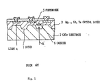
- a structure shown in Fig. 1 where a CdTe substrate 2 is provided with ditches 1 at a predetermined pitch, where a crystal layer 3 is formed of, for example, an epitaxial growth of p-type Hg 1-x Cd x Te upon the substrate.
- a photodiode 5 is formed of a pn junction having an n + layer 4 doped with an impurity atom of a conductivity type opposite to the conductivity type of Hg 1-x Cd x Te crystal layer 3.
- a plurality of photodiodes 5 are formed over the portion excluding ditches 1 of substrate 2.
- Carriers generated by an infrared light A' input to ditch 1 are trapped in Hg 1-x Cd x Te crystal layer 3 thick at the ditch on the way to reach a nearby pn junction.
- trapped carriers prevent a crosstalk between signals detected in the adjacent photodiodes 5.
- trapping of the carriers causes deterioration of detection sensitivity of the photodiodes.
- a photocell of the photoelectric transducer of the present invention as defined in claim 1 comprises a photodiode region doped with an impurity of a conductivity type opposite to that of the compound semiconductor substrate of the photoelectric transducer.
- An enclosure region is formed by the same doping as the photodiode region, surrounding and apart from the photodiode region.
- a gate electrode is provided, on an insulation layer formed all over the surface of the photodiode and the enclosure, over a portion in between the photodiode and the enclosure region. The enclosure region is connected via a contact hole through the insulation layer and a first switch to a ground level.
- the gate electrode is connected via a second switch to a predetermined voltage whose polarity is the same as the conductivity type of the compound semiconductor substrate.
- the first switch On a high-resolution mode, the first switch is closed and the second switch is open, so that the grounded enclosure prevents carrier generated in between the photodiode and the enclosure region from flowing into an adjacent cell.
- the first switch On a high-sensitivity mode, the first switch is open and the second switch is closed, so that the gate voltage generates a channel to electrically connect the photodiode to the enclosure region, so that the carriers generated within the enclosure are all gathered to the photodiode.
- the first and second switches may be fabricated on a second semiconductor substrate arranged over the compound semiconductor substrate. The second substrate is electrically connected via bumps to the photodiode, the gate electrode and the enclosure region.
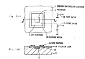
- a substrate 11 formed of, for example, p-type PbSnTe (lead-tin-tellurium) compound semiconductor
- In (indium) atoms which are of n-type, are doped so as to form a photodiode 12.
- a predetermined enclosure region 13 surrounding but apart from the island 12 on the substrate surface is also doped with the In atoms.
- An insulation layer 14 typically of ZnS (zinc sulfide) is formed upon the surface of substrate 11 having thus doped regions 12 and 13.
- a gate electrode 15 is formed so as to cover the portion in between photodiode 12 and enclosure region 13.
- An infrared light A to be detected is input from the bottom of substrate 11.
- Enclosure region 13 is lead out through insulation layer 14 via a first switch 22 to ground 21.
- Gate electrode 15 is connected via a second switch 23 to a positive DC (direct current) voltage source.
- first switch 22 is closed so as to make enclosure region 13 grounded and second switch 23 is opened so as to make gate electrode 15 floated, as shown in Fig. 3(a).
- Carriers generated in the vicinity of enclosure region 13 are attracted and absorbed by the junction potential of enclosure region 13.
- the movements of the carriers are illustrated with small arrows in Figs. 3.
- no carriers flow into adjacent photo diode, which is not shown in the figure, causing no crosstalk between the adjacent photo cells.
- a decrease in the amount of carriers detected by photo diode 12 cannot be helped, due to the fact that some of the carriers generated in between the photodidode and the enclosure are absorbed by the elclosure.
- first switch 22 is opened so as to make enclosure 13 floated and second switch 23 is closed so as to apply a positive voltage onto gate electrode 15, as shown in Fig. 3(b). Due to the positive voltage of gate electrode, the surface of substrate 11 beneath gate electrode 15 is inverted to n-type so as to form a channel 24. Channel 24 electrically connects enclosure region 13 to photodiode 12. Accordingly, all the carriers generated within enclosure region 13 are gathered by photo diode 12. Thus, the high sensitivity detection is accomplished.
- a preferred embodiment of the present invention is hereinafter described in detail.
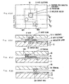
- a substrate 11 formed of, for example, a p-type PbSnTe (lead-tin-tellurium) compound semiconductor
- In (indium) atoms are doped by thermal diffusion or preferably by ion implantation, for example, as much as 10 17 /cm 3 to 10 18 /cm 3 , and 1 ⁇ m deep so as to form a photodiode 12 and enclosure region 13.
- Photodiode 12 is typically 20 ⁇ m square.
- Enclosure region 13 is of almost square walls, for example, 40 ⁇ m square, 3 ⁇ m width and 1 ⁇ m deep, surrounding but apart from photodiode 12.
- An insulation layer 14 typically of ZnS (zinc sulfide) is sputtered all over the surface of substrate 11 having thus doped portions 12 and 13, typically as thick as 0.5 ⁇ m.
- a gate electrode 15 typically of gold is patterned according to conventional sputtering and lithography techniques so as to substantially cover the portion in between photodiode 12 and enclosure 13.
- Contact holes 20 and 20A are opened, through insulation layer 14, over predetermined portions of photodiode 12 and enclosure region 13, respectively.
- Bumps 18, 18A and 18B are provided through contact holes 20 and 20A as well as on gate electrode 15.
- MOS FET metal-oxide-semiconductor field-effect-transistor
- CCD charge-coupled device
- gate electrode 15 covers the portion in between photo diodes 12 and enclosure region 13, the width of gate electrode does not strictly require to be equal to the width of the gap between gate electrode and the enclosure. An gate electrode wider than the gap causes no problem. If the gate electrode width is smaller than the gap, an increased electrode voltage can expands the width of the channel generated therebeneath until the channel reaches both the photo diode and the enclosure.
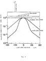
- Fig. 6 Reduction of the crosstalk by the existence of the enclosure is shown in Fig. 6.
- the abscissa indicates position of a light spot injected onto a sample substrate having a single photoelectric cell of dimensions of the above-described preferred embodiment, drawn at the top of the graph.
- the ordinate indicates relative sensitivity in arbitrary unit, for example, the output current of the photodiode. It is observed from the graph that the enclosure decreases the amount of carriers caught in the adjacent cell area down to almost one tenth of the amount of the case having no enclosure.
- the enclosure region is grounded by the first switch, the ground level may be replaced with an arbitrary proper voltage other than the ground level, as long as the enclosure region prevents the carriers from flowing into the adjacent cell.
- Voltage to be applied to gate electrode 15 is typically + 1 volt for the case of the above-described preferred embodiment.
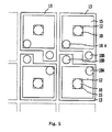
- FIG. 4 Many of the photocell shown in Figs. 4 are integrated as typically shown in Fig. 5.
- Each of enclosure region 13 is independently provided with the first switch 22. All of gate electrodes 23 are commonly connected to a single second switch 23.
- the photocells are arranged in a two-dimensional layout, it is apparent that the present invention can be applied to an photoelectric transducer having linearly arranged multiple photocells.
- the sides of enclosure region facing the sides of the linear arrangement may be omitted, while the enclosure regions at the side facing adjacent photocells are remaining as linear fences.
- the material of compound semiconductor is referred to as p-type PbSnTe, it is apparent that the present invention may be applied to a photoelectric device whose substrate is formed of InSb (indium-antimony), HgCdTe (mercury-cadnium-tellurium) or HgZnTe (mercury-zinc-tellurium).
Landscapes
- Solid State Image Pick-Up Elements (AREA)
- Light Receiving Elements (AREA)
Claims (8)
- Photoelektrischer Wandler mit einer Photodiodenzelle, wobei die Photozelle aufweist:ein Verbindungshalbleitersubstrat (11) eines ersten Leitungstyps;einen Photodiodenbereich (12), der mit einer Verunreinigung eines zweiten Leitungstyps dotiert ist, der dem ersten Leitungstyp entgegengesetzt ist, und auf einer Oberfläche des Verbindungshalbleitersubstrates vorgesehen ist;einen Einschließbereich (13), der den Photodiodenbereich (12) umgibt und von diesem beabstandet ist, mit einer Verunreinigung des zweiten Leitungstyps dotiert ist und auf der Oberfläche des Verbindungshalbleitersubstrates (11) vorgesehen ist;eine Isolationsschicht (14) auf der Oberfläche;eine Gateelektrode (15) auf der Isolationsschicht, wobei sich die Gateelektrode über einem Abschnitt zwischen dem Photodiodenbereich und dem Einschließbereich befindet;einen ersten Schalter (22) und einen zweiten Schalter (23), wobei der erste Schalter im geschlossenen Zustand eine erste vorbestimmte Spannung an den Einschließbereich anlegt, wenn ein hochauflösender Modus gewünscht ist und der zweite Schalter geöffnet ist, und der zweite Schalter im Schließzustand eine zweite vorbestimmte Spannung an die Gateelektrode (15) anlegt, wenn ein hochempfindlicher Modus erwünscht ist und der erste Schalter geöffnet ist.
- Photoelektrischer Wandler nach Anspruch 1,
bei dem die erste vorbestimmte Spannung eine Spannung des Verbindungshalbleitersubstrates (11) ist. - Photoelektrischer Wandler nach Anspruch 1 oder 2,
bei dem die Polarität der zweiten vorbestimmten Spannung gleich der Polarität des ersten Leitungstyps ist. - Photoelektrischer Wandler nach einem der Ansprüche 1 bis 3,
bei dem der Verbindungshalbleiter (11) aus einer Gruppe bestehend aus PbSnTe (BleiAntimon-Tellur), InSb (Indium-Antimon), HgCdTe (Quecksilber-Kadmium-Tellur) und HgZnTe (Quecksilber-Zink-Tellur) gewählt ist, wobei das zu erfassende Licht ein Infrarotlicht ist. - Photoelektrischer Wandler nach einem der Ansprüche 1 bis 4,
wobei der photoelektrische Wandler mehrere Photozellen aufweist. - Photoelektrischer Wandler nach Anspruch 5,
wobei die Photozellen linear angeordnet sind. - Photoelektrischer Wandler nach Anspruch 5,
wobei die Photozellen zweidimensional angeordnet sind. - Photoelektrischer Wandler nach einem der Ansprüche 1 bis 7,
weiterhin aufweisend ein zweites Halbleitersubstrat (16), das den ersten und den zweiten Schalter (22, 23) sowie eine Schaltung zur Verarbeitung von Signalen von der Photodiode (12) aufweist, wobei das zweite Halbleitersubstrat (16) über dem Verbindungshalbleiter (11) angeordnet ist und das zweite Halbleitersubstrat (16) elektrisch mit der Photodiode (12), dem Einschließbereich-Verbindungshalbleiter (13) und der Gateelektrode (15) mittels jeweiliger Erhebungen (18, 18A, 18B) verbunden ist.
Applications Claiming Priority (2)
| Application Number | Priority Date | Filing Date | Title |
|---|---|---|---|
| JP3012058A JPH04246860A (ja) | 1991-02-01 | 1991-02-01 | 光電変換装置 |
| JP12058/91 | 1991-02-01 |
Publications (2)
| Publication Number | Publication Date |
|---|---|
| EP0497326A1 EP0497326A1 (de) | 1992-08-05 |
| EP0497326B1 true EP0497326B1 (de) | 1996-12-18 |
Family
ID=11795003
Family Applications (1)
| Application Number | Title | Priority Date | Filing Date |
|---|---|---|---|
| EP92101488A Expired - Lifetime EP0497326B1 (de) | 1991-02-01 | 1992-01-29 | Photoelektrischer Umwandler schaltbar zwischen hochauflösenden und hochempfindlichen Modus |
Country Status (4)
| Country | Link |
|---|---|
| US (1) | US5196692A (de) |
| EP (1) | EP0497326B1 (de) |
| JP (1) | JPH04246860A (de) |
| DE (1) | DE69215914T2 (de) |
Families Citing this family (10)
| Publication number | Priority date | Publication date | Assignee | Title |
|---|---|---|---|---|
| JPH04104216A (ja) * | 1990-08-24 | 1992-04-06 | Hitachi Koki Co Ltd | 光走査装置 |
| US6043548A (en) * | 1993-04-14 | 2000-03-28 | Yeda Research And Development Co., Ltd. | Semiconductor device with stabilized junction |
| US5508625A (en) * | 1994-06-23 | 1996-04-16 | The Boeing Company | Voltage stand off characteristics of photoconductor devices |
| JP2746154B2 (ja) * | 1994-12-07 | 1998-04-28 | 日本電気株式会社 | 固体撮像素子 |
| US5998235A (en) | 1997-06-26 | 1999-12-07 | Lockheed Martin Corporation | Method of fabrication for mercury-based quaternary alloys of infrared sensitive materials |
| JP2001024270A (ja) * | 1999-07-06 | 2001-01-26 | Kyocera Corp | バーンイン用基板及びそれを用いたバーンイン方法 |
| GB0218713D0 (en) * | 2002-08-12 | 2002-09-18 | Mitel Knowledge Corp | Architecture and Implementation for control of context aware call processing with local feature definition |
| DE102005049228B4 (de) * | 2005-10-14 | 2014-03-27 | Siemens Aktiengesellschaft | Detektor mit einem Array von Photodioden |
| JP2007165621A (ja) * | 2005-12-14 | 2007-06-28 | Toshiba Corp | 光結合装置 |
| JP4993941B2 (ja) * | 2006-04-27 | 2012-08-08 | パナソニック株式会社 | 半導体集積回路及びこれを備えたシステムlsi |
Family Cites Families (8)
| Publication number | Priority date | Publication date | Assignee | Title |
|---|---|---|---|---|
| US3703669A (en) * | 1971-08-12 | 1972-11-21 | Motorola Inc | Photocurrent cross talk isolation |
| JPS55112081A (en) * | 1979-02-21 | 1980-08-29 | Hitachi Ltd | Solid state pickup device |
| US4369372A (en) * | 1979-06-18 | 1983-01-18 | Canon Kabushiki Kaisha | Photo electro transducer device |
| JPS5712571A (en) * | 1980-06-27 | 1982-01-22 | Toshiba Corp | Semiconductor photodetector |
| JPS58148455A (ja) * | 1982-02-16 | 1983-09-03 | ゼロツクス・コ−ポレ−シヨン | ポリシリコン隔離ホトダイオ−ドアレイ撮像装置 |
| US4531055A (en) * | 1983-01-05 | 1985-07-23 | The United States Of America As Represented By The Secretary Of The Air Force | Self-guarding Schottky barrier infrared detector array |
| JPS62122268A (ja) * | 1985-11-22 | 1987-06-03 | Fuji Photo Film Co Ltd | 固体撮像素子 |
| US4751560A (en) * | 1986-02-24 | 1988-06-14 | Santa Barbara Research Center | Infrared photodiode array |
-
1991
- 1991-02-01 JP JP3012058A patent/JPH04246860A/ja not_active Withdrawn
-
1992
- 1992-01-24 US US07/825,497 patent/US5196692A/en not_active Expired - Fee Related
- 1992-01-29 DE DE69215914T patent/DE69215914T2/de not_active Expired - Fee Related
- 1992-01-29 EP EP92101488A patent/EP0497326B1/de not_active Expired - Lifetime
Also Published As
| Publication number | Publication date |
|---|---|
| DE69215914T2 (de) | 1997-06-26 |
| DE69215914D1 (de) | 1997-01-30 |
| EP0497326A1 (de) | 1992-08-05 |
| JPH04246860A (ja) | 1992-09-02 |
| US5196692A (en) | 1993-03-23 |
Similar Documents
| Publication | Publication Date | Title |
|---|---|---|
| KR100262774B1 (ko) | 상부 버스 가상 위상 프레임 행간 전송 ccd 영상 감지기 | |
| CA1298389C (en) | High dynamic range charge-coupled device | |
| US4373167A (en) | Solid state image sensor with overflow protection and high resolution | |
| US4173765A (en) | V-MOS imaging array | |
| US5070380A (en) | Transfer gate for photodiode to CCD image sensor | |
| US4733286A (en) | Semiconductor photoelectric converting device | |
| US11296239B2 (en) | Surface MESFET | |
| EP0544260A1 (de) | Überlaufvorrichtung für einen CCD-Bildsensor | |
| CA1096498A (en) | Ccd radiation sensor | |
| EP0497326B1 (de) | Photoelektrischer Umwandler schaltbar zwischen hochauflösenden und hochempfindlichen Modus | |
| EP0186162A2 (de) | Festkörperbildsensor | |
| US4213137A (en) | Monolithic variable size detector | |
| US4499590A (en) | Semiconductor circuit for compressing the dynamic range of a signal | |
| US4974043A (en) | Solid-state image sensor | |
| US4488165A (en) | Extrinsic infrared detector with a charge reset function | |
| US4760435A (en) | Anti-blooming drain structure in charge coupled device image sensors | |
| US4321614A (en) | Radiant energy sensor with blooming control | |
| AU596782B1 (en) | Imaging devices, elements and systems | |
| US5066994A (en) | Image sensor | |
| EP0271522A1 (de) | Blockierten störstellenbanddetektor mit rückseitenkontakt | |
| US5155362A (en) | Infra-red radiation imaging device arrangements | |
| JP2540834B2 (ja) | Mos型イメ−ジセンサ | |
| KR950010532B1 (ko) | Ccd의 구조 | |
| US5665998A (en) | Geometric enhancement of photodiodes for low dark current operation | |
| WO1989005039A1 (en) | Blooming control in ccd image sensors |
Legal Events
| Date | Code | Title | Description |
|---|---|---|---|
| PUAI | Public reference made under article 153(3) epc to a published international application that has entered the european phase |
Free format text: ORIGINAL CODE: 0009012 |
|
| AK | Designated contracting states |
Kind code of ref document: A1 Designated state(s): DE FR GB NL |
|
| 17P | Request for examination filed |
Effective date: 19920921 |
|
| GRAG | Despatch of communication of intention to grant |
Free format text: ORIGINAL CODE: EPIDOS AGRA |
|
| 17Q | First examination report despatched |
Effective date: 19960329 |
|
| GRAH | Despatch of communication of intention to grant a patent |
Free format text: ORIGINAL CODE: EPIDOS IGRA |
|
| GRAH | Despatch of communication of intention to grant a patent |
Free format text: ORIGINAL CODE: EPIDOS IGRA |
|
| GRAA | (expected) grant |
Free format text: ORIGINAL CODE: 0009210 |
|
| AK | Designated contracting states |
Kind code of ref document: B1 Designated state(s): DE FR GB NL |
|
| REF | Corresponds to: |
Ref document number: 69215914 Country of ref document: DE Date of ref document: 19970130 |
|
| ET | Fr: translation filed | ||
| PLBE | No opposition filed within time limit |
Free format text: ORIGINAL CODE: 0009261 |
|
| STAA | Information on the status of an ep patent application or granted ep patent |
Free format text: STATUS: NO OPPOSITION FILED WITHIN TIME LIMIT |
|
| 26N | No opposition filed | ||
| REG | Reference to a national code |
Ref country code: GB Ref legal event code: IF02 |
|
| PGFP | Annual fee paid to national office [announced via postgrant information from national office to epo] |
Ref country code: FR Payment date: 20030110 Year of fee payment: 12 |
|
| PGFP | Annual fee paid to national office [announced via postgrant information from national office to epo] |
Ref country code: GB Payment date: 20030129 Year of fee payment: 12 |
|
| PGFP | Annual fee paid to national office [announced via postgrant information from national office to epo] |
Ref country code: NL Payment date: 20030130 Year of fee payment: 12 |
|
| PGFP | Annual fee paid to national office [announced via postgrant information from national office to epo] |
Ref country code: DE Payment date: 20030206 Year of fee payment: 12 |
|
| PG25 | Lapsed in a contracting state [announced via postgrant information from national office to epo] |
Ref country code: GB Free format text: LAPSE BECAUSE OF NON-PAYMENT OF DUE FEES Effective date: 20040129 |
|
| PG25 | Lapsed in a contracting state [announced via postgrant information from national office to epo] |
Ref country code: NL Free format text: LAPSE BECAUSE OF NON-PAYMENT OF DUE FEES Effective date: 20040801 |
|
| PG25 | Lapsed in a contracting state [announced via postgrant information from national office to epo] |
Ref country code: DE Free format text: LAPSE BECAUSE OF NON-PAYMENT OF DUE FEES Effective date: 20040803 |
|
| GBPC | Gb: european patent ceased through non-payment of renewal fee |
Effective date: 20040129 |
|
| PG25 | Lapsed in a contracting state [announced via postgrant information from national office to epo] |
Ref country code: FR Free format text: LAPSE BECAUSE OF NON-PAYMENT OF DUE FEES Effective date: 20040930 |
|
| NLV4 | Nl: lapsed or anulled due to non-payment of the annual fee |
Effective date: 20040801 |
|
| REG | Reference to a national code |
Ref country code: FR Ref legal event code: ST |