EP0498373A2 - Télévision avec circuit de déviation synchrone - Google Patents
Télévision avec circuit de déviation synchrone Download PDFInfo
- Publication number
- EP0498373A2 EP0498373A2 EP92101831A EP92101831A EP0498373A2 EP 0498373 A2 EP0498373 A2 EP 0498373A2 EP 92101831 A EP92101831 A EP 92101831A EP 92101831 A EP92101831 A EP 92101831A EP 0498373 A2 EP0498373 A2 EP 0498373A2
- Authority
- EP
- European Patent Office
- Prior art keywords
- horizontal
- power supply
- synchronous
- circuit
- signal
- Prior art date
- Legal status (The legal status is an assumption and is not a legal conclusion. Google has not performed a legal analysis and makes no representation as to the accuracy of the status listed.)
- Granted
Links
Images


Classifications
-
- H—ELECTRICITY
- H04—ELECTRIC COMMUNICATION TECHNIQUE
- H04N—PICTORIAL COMMUNICATION, e.g. TELEVISION
- H04N3/00—Scanning details of television systems; Combination thereof with generation of supply voltages
- H04N3/10—Scanning details of television systems; Combination thereof with generation of supply voltages by means not exclusively optical-mechanical
- H04N3/16—Scanning details of television systems; Combination thereof with generation of supply voltages by means not exclusively optical-mechanical by deflecting electron beam in cathode-ray tube, e.g. scanning corrections
- H04N3/18—Generation of supply voltages, in combination with electron beam deflecting
-
- H—ELECTRICITY
- H04—ELECTRIC COMMUNICATION TECHNIQUE
- H04N—PICTORIAL COMMUNICATION, e.g. TELEVISION
- H04N5/00—Details of television systems
- H04N5/63—Generation or supply of power specially adapted for television receivers
Definitions
- This invention relates to a television synchronous deflection circuit, and more specifically to such a circuit for securing a stable operation when power is initially supplied.
- a typical conventional television receiver is generally comprised of a tuner for selecting a desired channel signal among VHF and UHF television signals received via an antenna and for converting the selected channel signal into an intermediate-frequency signal, a picture intermediate-frequency amplifier for amplifying the picture intermediate-frequency signal, a detector for detecting the amplified picture signal outputted from the picture intermediate-frequency amplifier and for outputting a composite picture signal, a synchronous separator for separating a horizontal synchronous signal from the output signal of the detector, a horizontal deflector for generating a horizontal deflection signal which is to be applied to the horizontal deflecting coil of a cathode-ray tube and which is based on the horizontal synchronous signal separated by the synchronous separator, a color signal processing circuit for generating the necessary three primary color signals (i.e. red, green and blue) from color picture signals, as well as other signal processing circuits.
- a tuner for selecting a desired channel signal among VHF and UHF television signals received via an antenna and for converting the selected channel signal into an intermediate-
- a horizontal AFC Automatic Frequency Control circuit for eliminating noise pulses in the horizontal synchronous signal outputted from the synchronous separator and for preventing any shift in horizontal synchronization.
- the horizontal deflector is operable upon receipt of the D.C. current obtained from a commercial power supply (e.g., 50 Hz/100 V) by diode rectification.
- a commercial power supply e.g., 50 Hz/100 V
- circuit blocks such as the picture intermediate-frequency amplifier, detector, synchronous separator and color signal processing circuit are operable upon receipt of the D.C. current from a second power supply obtained by smoothing a high-frequency flyback pulse obtained from a flyback transformer for the generation of an anode voltage for the cathode-ray tube.
- the second power supply is built up. But since the quantity of charging electric charges of a capacitor in the synchronous separator is small before the output voltage of the second power supply reaches a predetermined voltage, a charging current from the second power supply flows to the capacitor, and as a result, an abnormal signal (i.e. not a correct horizontal synchronous signal) would be outputted from the synchronous separator. Therefore the horizontal AFC circuit would output an abnormal frequency signal missing the safe operating region of a backward horizontal output transistor.
- a television synchronous deflection circuit is comprised of: a first power supply circuit for supplying a D.C.
- a second power supply circuit for smoothing the flyback pulse and for supplying a predetermined D.C. voltage to the synchronous separator; a comparator for comparing the output voltages of the first and second power supply circuits with each other; and a control circuit for controlling the operation of the horizontal AFC circuit according to a comparison signal outputted from the comparator.
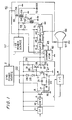
- FIG. 1 shows a television synchronous deflection circuit embodying this invention and its peripheral circuits.
- picture and audio intermediate-frequency signals outputted from a mixer (not shown) of a front-stage tuner are inputted to a picture intermediate-frequency amplifier (hereinafter also called IF) 11.
- the amplified picture signal from the IF 11 is detected by a picture detector (hereinafter also called DET) 12 and is then outputted as a composite picture signal as shown in FIG. 5(a).
- DET picture detector
- t1 designates the duration of a horizontal synchronous signal
- t2 designates the duration of a picture signal.
- a D.C. voltage of about 12 V is applied from a second power supply 2.
- the second power supply 2 includes a smoothing circuit 102 for smoothing a high-frequency flyback pulse 57 outputted from the secondary side of a flyback transformer 55 described below, and a regulator 103 for regulating the output of the smoothing circuit 102 and for outputting a D.C. voltage of about 12 V.
- the composite picture signal from the picture detector 12 is inputted to the base of an n-p-n transistor 13 and to a color signal processing circuit (hereinafter also called Y/C) 14.
- the transistor 13 is connected at the collector to the second power supply 2 and is connected at the emitter to ground via a resistor 16 and to a subsequent-stage synchronous separator 20 via a resistor 17.
- a resistor 17 is connected to one end of the parallel combination of a capacitor 21 and a resistor 22, and to the other is connected the emitter of an n-p-n transistor 23.
- the collector of the transistor 23 is connected to diodes 24, 25 in series in this order toward the second power supply 2 and is also connected to the base of a p-n-p transistor 28.
- the base of the transistor 23 is connected to a junction of resistors 26, 27 interconnected in series between the second power supply 2 and ground.
- the emitter of the transistor 28 is connected to the second power supply 2 via a resistor 29 and is connected to the base via a resistor 31.
- the collector of the transistor 28 is connected to the ground via a resistor 32.
- This synchronous separator 20 samples a pulse-like horizontal synchronous signal 33 such as is shown in FIG. 5(d), and outputs this sample from the collector of the transistor 28 to a subsequent-stage horizontal deflector 40.
- the horizontal synchronous signal from the synchronous separator 20 is inputted to a horizontal AFC circuit 41 of the horizontal deflector 40 and is processed there so as to eliminate noise pulses of signals other than the horizontal synchronous signal and to prevent any displacement in horizontal synchronization.
- a comparison signal 43 is inputted from a comparator 42.
- the comparator 42 compares the second reference voltage V ref2 according to the output voltage of the second power supply 2 with the first reference voltage V ref1 according to the output voltage of the first power supply 1 and outputs a comparison signal 43 of "L" level when V ref2 > V ref1 .
- the first power supply 1 is equipped with a main switch 68.
- a commercial A.C. voltage (100 V and 50 or 60 Hz) supply is inputted from a socket 67.
- the A.C. voltage is rectified by rectifier diodes 61 - 64 smoothed by capacitor 65 and by a regulator 66, whereupon the resulting voltage is outputted as a D.C. voltage of about 100 V.
- the horizontal AFC circuit 41 is connected to a horizontal driving circuit 45 for amplifying a pulse voltage of the horizontal synchronous signal and for shaping a waveform of the horizontal synchronous signal, and the horizontal driving circuit 45 is connected to a horizontal output circuit 46.
- the output voltage from the first power supply 1 is applied to the horizontal AFC circuit 41, the horizontal driving circuit 45 and the horizontal output circuit 46, after being dropped to 7 - 8 V by a resistor 47.
- a horizontal oscillatory output from the horizontal output circuit 46 is applied to the base of a horizontal predrive transistor 51.
- the collector of the horizontal predrive transistor 51 is connected to the first power supply 1 via the primary coil of a horizontal drive transformer 52 and a resistor 53, while the emitter is grounded
- the secondary coil of the horizontal drive transformer 52 is connected at one end to the base of a horizontal drive transistor 54 and at the other to ground.
- the collector of the horizontal drive transistor 54 is connected to the first power supply 1 via the primary coil of the flyback transformer 55 and the horizontal deflecting coil 57 of the cathode-ray tube 56, while the emitter is grounded.
- a high-frequency (about 15.7 KHz) flyback pulse 57 is generated and is then supplied to the second power supply 2.
- a high-voltage (about 20 - 30 kV) anode voltage is generated and is then applied to an anode (not shown) of the cathode-ray tube 56.
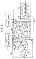
- FIG. 4 is a detailed circuit diagram showing the comparator 42 and the horizontal AFC circuit 41 as well as their peripheral circuits.
- parts or elements similar to those of FIG. 1 are designated by like reference numerals and their description is omitted for clarity.
- the comparator 42 includes a comparing circuit 70 composed of two n-p-n transistors 71, 72 connected at their emitters to a constant current power supply 73.
- the base of the first transistor 71 is connected to the first power supply 1 via a resistor 77 and is connected to ground via diodes 78, 79 interconnected in series in this order, and the collector is connected to a mirror circuit 80.
- the base of the second transistor 72 is connected through the series diodes 74, 75 to the second power supply 2 and is connected to ground via a resistor 76, while the collector is connected directly to the second power supply 2.
- the mirror circuit 80 includes p-n-p transistors 81, 82 whose bases are connected to each other and whose emitters are connected to the first power supply 1.
- the collector of the transistor 81 is connected to its base and also to the collector of the transistor 71 of the comparing circuit 70.
- the collector of the transistor 82 is connected to ground via a resistor 83; from the collector of transistor 82, a comparison signal of a predetermined level is outputted so as to open and close a switch 94 located in the horizontal AFC circuit 41. The switch 94 will be closed when the comparison signal 43 is at an "L" level.
- the horizontal AFC circuit 41 is equipped with a phase comparator (PC) 91 whose output side is connected to a voltage controlled oscillator (VCO) 93 via a low-pass filter (LPF) 92. These circuits are activated by the voltage applied from the first power supply 1.
- PC phase comparator
- VCO voltage controlled oscillator
- LPF low-pass filter
- the phase comparator 91 To the phase comparator 91, the branched output of the voltage controlled oscillator 93 is inputted, as well as the horizontal synchronous signal 33 from the synchronous separator 20, when the switch 94 is closed.
- the phase comparator 91 compares the phase of the output from the voltage controlled oscillator 93 with the horizontal synchronous signal 33 and, in order to minimize the phase difference, a control voltage is supplied to the voltage controlled oscillator 93.
- the output from the voltage controlled oscillator 93 is supplied to the subsequent-stage horizontal driving circuit 45 (FIG. 1).
- the potential at point B is increased so that the current I1 will not flow, and so turn off the transistor 23.
- the electric charge accumulated in the capacitor 21 is discharged via the resistor 22 so that a current I2 satisfying the following equation (1) will flow.
- I1 x t1 I2 x t2 (1) Therefore, during the duration of t2 of the picture signal, the potential at point C will be V cc (as shown in FIG. 5(c)) in order to turn the transistor 28 off so that the potential at point D will be the ground level (GND).
- the synchronous separator 20 outputs a pulse-like horizontal synchronous signal 33 such as shown in FIG. 5(d) to the horizontal AFC circuit 41.
- the synchronous deflection circuit When the power supply of the television receiver is turned on, the synchronous deflection circuit will operate as follows: When the main switch of the first power supply 1 (FIG. 2) is closed, full wave rectification of 100 V A.C. occurs, and a D.C. voltage of about 100 V is applied to the flyback transformer 55. As a result, a flyback pulse 57 is generated at the secondary coil 58 of the flyback transformer 55 and is then supplied to the second power supply 2. Therefore there is a delay from when the first power supply 1 is activated to when the second power supply 2 is activated.
- the output voltage V ref1 of the first power source 1 is applied to the base (point F) of the first transistor 71 of the comparing circuit 70, while the base (point E) of the second transistor 72 is at the ground potential. Therefore only the first transistor 71 is turned on to activate the mirror circuit 80.
- the transistor 81 of the mirror 80 is also turned on so that current will flow between its emitter and collector. Also the transistor 82 of the mirror circuit 80 is turned on so that the current through it is equal to the current flowing through both the transistor 81 and the first transistor 71. In this case, the potential at point G (namely the comparison signal 43) will be a "H" level so that the switch 94 will be opened.
- the second power supply 2 When the second power supply 2 has start operating, its output voltage is increased in order to progressively increase the second reference voltage V ref2 . After the lapse of a predetermined time, a stable D.C. voltage of about 12 V is outputted from the second power source 2 and is applied to the synchronous separator 20 and various other elements.
- V ref2 the second reference voltage
- V ref2 the potential at point B is reduced so that the current I1 will flow to turn the transistor 23 on.
- the transistor 28 is also turned on so that the potential at point D will be a "H" level.
- the synchronous separator 20 is activated, irrespective of the picture signal, so that an abnormal signal will be applied to the horizontal AFC circuit 41.
- phase comparator 91 since only one input, namely, only the output of the voltage controlled oscillator 93, is applied to the phase comparator 91, the phase comparator 91 becomes unable to compare so that its output voltage and the output of the low-pass filter 92 will be a bias voltage only. Therefore, the output from the voltage controlled oscillator 93 will be in a free-run state and hence stable.
- the operation of the horizontal AFC circuit 41 is stabilized by the provision of the switch 94.
- Various stabilization methods may be adopted; for example, the output of the voltage controlled oscillator 93 may be adjusted to a stable oscillation form.
- the switch 94 may a transistor or another device.
- this invention it is possible to prevent any abnormal operation of the horizontal AFC circuit when the power supply of the television receiver is switched on so that a stable operation of the horizontal output transistor can be secured. Further, to realize this, it is only necessary to add control circuits such as a comparator and a switch, which do not substantially increase the total number of elements or parts, thus avoiding an increase of manufacturing cost.
Landscapes
- Engineering & Computer Science (AREA)
- Multimedia (AREA)
- Signal Processing (AREA)
- Details Of Television Scanning (AREA)
- Synchronizing For Television (AREA)
- Television Receiver Circuits (AREA)
Applications Claiming Priority (2)
| Application Number | Priority Date | Filing Date | Title |
|---|---|---|---|
| JP18003/91 | 1991-02-08 | ||
| JP3018003A JP2562732B2 (ja) | 1991-02-08 | 1991-02-08 | テレビジョン受像機 |
Publications (3)
| Publication Number | Publication Date |
|---|---|
| EP0498373A2 true EP0498373A2 (fr) | 1992-08-12 |
| EP0498373A3 EP0498373A3 (en) | 1993-01-13 |
| EP0498373B1 EP0498373B1 (fr) | 1996-06-05 |
Family
ID=11959523
Family Applications (1)
| Application Number | Title | Priority Date | Filing Date |
|---|---|---|---|
| EP92101831A Expired - Lifetime EP0498373B1 (fr) | 1991-02-08 | 1992-02-04 | Télévision avec circuit de déviation synchrone |
Country Status (5)
| Country | Link |
|---|---|
| US (1) | US5208517A (fr) |
| EP (1) | EP0498373B1 (fr) |
| JP (1) | JP2562732B2 (fr) |
| KR (1) | KR0156009B1 (fr) |
| DE (1) | DE69211170T2 (fr) |
Families Citing this family (4)
| Publication number | Priority date | Publication date | Assignee | Title |
|---|---|---|---|---|
| DE4425526C2 (de) * | 1993-07-27 | 2001-02-15 | Samsung Electronics Co Ltd | Videorekorder mit einem Anschluß für einen Gebührenfernsehdecodierer |
| JP3250785B2 (ja) * | 1996-08-09 | 2002-01-28 | アルプス電気株式会社 | テレビチューナ |
| KR100371379B1 (ko) * | 1997-10-09 | 2003-03-26 | 주식회사 엘지이아이 | 영상표시기기의씨알티전면vlf방사전계차폐장치 |
| JPH11205627A (ja) * | 1998-01-19 | 1999-07-30 | Sony Corp | 水平偏向装置、自動周波数制御装置および映像信号受信装置 |
Family Cites Families (3)
| Publication number | Priority date | Publication date | Assignee | Title |
|---|---|---|---|---|
| US3956669A (en) * | 1974-10-29 | 1976-05-11 | Quasar Electronics Corporation | Standby power supply |
| US4188568A (en) * | 1978-08-14 | 1980-02-12 | Gte Sylvania Incorporated | Power saving circuit |
| FR2607991B1 (fr) * | 1986-12-05 | 1989-02-03 | Radiotechnique Ind & Comm | Alimentation a decoupage pour un televiseur muni d'un systeme de veille |
-
1991
- 1991-02-08 JP JP3018003A patent/JP2562732B2/ja not_active Expired - Fee Related
-
1992
- 1992-02-03 US US07/829,328 patent/US5208517A/en not_active Expired - Lifetime
- 1992-02-04 DE DE69211170T patent/DE69211170T2/de not_active Expired - Fee Related
- 1992-02-04 EP EP92101831A patent/EP0498373B1/fr not_active Expired - Lifetime
- 1992-02-07 KR KR1019920001791A patent/KR0156009B1/ko not_active Expired - Fee Related
Also Published As
| Publication number | Publication date |
|---|---|
| EP0498373B1 (fr) | 1996-06-05 |
| US5208517A (en) | 1993-05-04 |
| KR0156009B1 (ko) | 1998-11-16 |
| EP0498373A3 (en) | 1993-01-13 |
| DE69211170D1 (de) | 1996-07-11 |
| JP2562732B2 (ja) | 1996-12-11 |
| DE69211170T2 (de) | 1997-01-30 |
| JPH04257168A (ja) | 1992-09-11 |
| KR920017443A (ko) | 1992-09-26 |
Similar Documents
| Publication | Publication Date | Title |
|---|---|---|
| US3956669A (en) | Standby power supply | |
| CA2061166C (fr) | Appareil de television a circuit de protection du kinescope contre les brulures par le spot a grande constante de temps de coupure du courant de grille | |
| US4115812A (en) | Automatic gain control circuit | |
| US3519741A (en) | Regulated high voltage power supply | |
| US5017844A (en) | Disabling arrangement for a circuit operating at a deflection rate | |
| US6140881A (en) | Display apparatus with a circuit for controlling the input voltage of PLL according to display mode and method | |
| EP0498373A2 (fr) | Télévision avec circuit de déviation synchrone | |
| US4385264A (en) | Start-up circuit for a power supply | |
| US5561354A (en) | Horizontal deflection | |
| KR820001002B1 (ko) | 피이크 검파기 회로 | |
| US5047698A (en) | High voltage shutdown circuit | |
| JPS623640B2 (fr) | ||
| JPH0582110B2 (fr) | ||
| KR970005223B1 (ko) | 고압안정화 회로 | |
| US4612574A (en) | Oscillator-frequency control interface circuit | |
| US3414667A (en) | Beam current stabilizing circuit | |
| US4882624A (en) | Synchronizing signal separation circuit for a television receiver | |
| EP0269741A1 (fr) | Circuit pour generer des impulsions de synchronisation verticale | |
| US4385320A (en) | Automatic frequency control circuit | |
| US6233023B1 (en) | Automatic fine tuning circuit | |
| US20090027145A1 (en) | receiver comprising two tunners | |
| EP0390183B1 (fr) | Circuit de séparation du signal de synchronisation | |
| KR880000906B1 (ko) | 텔레비젼 표시장치 | |
| US4530005A (en) | AFC circuit for television tuner | |
| KR0130809Y1 (ko) | 텔레비전수상기의 과전압에 대한 튜너보호회로 |
Legal Events
| Date | Code | Title | Description |
|---|---|---|---|
| PUAI | Public reference made under article 153(3) epc to a published international application that has entered the european phase |
Free format text: ORIGINAL CODE: 0009012 |
|
| AK | Designated contracting states |
Kind code of ref document: A2 Designated state(s): DE FR GB |
|
| PUAL | Search report despatched |
Free format text: ORIGINAL CODE: 0009013 |
|
| AK | Designated contracting states |
Kind code of ref document: A3 Designated state(s): DE FR GB |
|
| 17P | Request for examination filed |
Effective date: 19930310 |
|
| 17Q | First examination report despatched |
Effective date: 19950309 |
|
| GRAH | Despatch of communication of intention to grant a patent |
Free format text: ORIGINAL CODE: EPIDOS IGRA |
|
| GRAH | Despatch of communication of intention to grant a patent |
Free format text: ORIGINAL CODE: EPIDOS IGRA |
|
| GRAA | (expected) grant |
Free format text: ORIGINAL CODE: 0009210 |
|
| AK | Designated contracting states |
Kind code of ref document: B1 Designated state(s): DE FR GB |
|
| REF | Corresponds to: |
Ref document number: 69211170 Country of ref document: DE Date of ref document: 19960711 |
|
| ET | Fr: translation filed | ||
| PLBE | No opposition filed within time limit |
Free format text: ORIGINAL CODE: 0009261 |
|
| STAA | Information on the status of an ep patent application or granted ep patent |
Free format text: STATUS: NO OPPOSITION FILED WITHIN TIME LIMIT |
|
| 26N | No opposition filed | ||
| REG | Reference to a national code |
Ref country code: GB Ref legal event code: IF02 |
|
| PGFP | Annual fee paid to national office [announced via postgrant information from national office to epo] |
Ref country code: DE Payment date: 20090129 Year of fee payment: 18 |
|
| PGFP | Annual fee paid to national office [announced via postgrant information from national office to epo] |
Ref country code: GB Payment date: 20090204 Year of fee payment: 18 |
|
| PGFP | Annual fee paid to national office [announced via postgrant information from national office to epo] |
Ref country code: FR Payment date: 20090213 Year of fee payment: 18 |
|
| GBPC | Gb: european patent ceased through non-payment of renewal fee |
Effective date: 20100204 |
|
| REG | Reference to a national code |
Ref country code: FR Ref legal event code: ST Effective date: 20101029 |
|
| PG25 | Lapsed in a contracting state [announced via postgrant information from national office to epo] |
Ref country code: FR Free format text: LAPSE BECAUSE OF NON-PAYMENT OF DUE FEES Effective date: 20100301 |
|
| PG25 | Lapsed in a contracting state [announced via postgrant information from national office to epo] |
Ref country code: DE Free format text: LAPSE BECAUSE OF NON-PAYMENT OF DUE FEES Effective date: 20100901 |
|
| PG25 | Lapsed in a contracting state [announced via postgrant information from national office to epo] |
Ref country code: GB Free format text: LAPSE BECAUSE OF NON-PAYMENT OF DUE FEES Effective date: 20100204 |