EP0498534B1 - Circuit de génération de configurations de nombres aléatoires artificiels - Google Patents
Circuit de génération de configurations de nombres aléatoires artificiels Download PDFInfo
- Publication number
- EP0498534B1 EP0498534B1 EP92300256A EP92300256A EP0498534B1 EP 0498534 B1 EP0498534 B1 EP 0498534B1 EP 92300256 A EP92300256 A EP 92300256A EP 92300256 A EP92300256 A EP 92300256A EP 0498534 B1 EP0498534 B1 EP 0498534B1
- Authority
- EP
- European Patent Office
- Prior art keywords
- flip
- operation mode
- artificial random
- output
- flop
- Prior art date
- Legal status (The legal status is an assumption and is not a legal conclusion. Google has not performed a legal analysis and makes no representation as to the accuracy of the status listed.)
- Expired - Lifetime
Links
Images


Classifications
-
- G—PHYSICS
- G01—MEASURING; TESTING
- G01R—MEASURING ELECTRIC VARIABLES; MEASURING MAGNETIC VARIABLES
- G01R31/00—Arrangements for testing electric properties; Arrangements for locating electric faults; Arrangements for electrical testing characterised by what is being tested not provided for elsewhere
- G01R31/28—Testing of electronic circuits, e.g. by signal tracer
- G01R31/317—Testing of digital circuits
- G01R31/3181—Functional testing
- G01R31/3183—Generation of test inputs, e.g. test vectors, patterns or sequences
- G01R31/318385—Random or pseudo-random test pattern
-
- G—PHYSICS
- G01—MEASURING; TESTING
- G01R—MEASURING ELECTRIC VARIABLES; MEASURING MAGNETIC VARIABLES
- G01R31/00—Arrangements for testing electric properties; Arrangements for locating electric faults; Arrangements for electrical testing characterised by what is being tested not provided for elsewhere
- G01R31/28—Testing of electronic circuits, e.g. by signal tracer
- G01R31/317—Testing of digital circuits
- G01R31/31712—Input or output aspects
- G01R31/31715—Testing of input or output circuits; test of circuitry between the I/C pins and the functional core, e.g. testing of input or output driver, receiver, buffer
-
- G—PHYSICS
- G01—MEASURING; TESTING
- G01R—MEASURING ELECTRIC VARIABLES; MEASURING MAGNETIC VARIABLES
- G01R31/00—Arrangements for testing electric properties; Arrangements for locating electric faults; Arrangements for electrical testing characterised by what is being tested not provided for elsewhere
- G01R31/28—Testing of electronic circuits, e.g. by signal tracer
- G01R31/317—Testing of digital circuits
- G01R31/3181—Functional testing
- G01R31/31813—Test pattern generators
-
- G—PHYSICS
- G06—COMPUTING OR CALCULATING; COUNTING
- G06F—ELECTRIC DIGITAL DATA PROCESSING
- G06F11/00—Error detection; Error correction; Monitoring
- G06F11/22—Detection or location of defective computer hardware by testing during standby operation or during idle time, e.g. start-up testing
- G06F11/26—Functional testing
- G06F11/27—Built-in tests
-
- G—PHYSICS
- G06—COMPUTING OR CALCULATING; COUNTING
- G06F—ELECTRIC DIGITAL DATA PROCESSING
- G06F7/00—Methods or arrangements for processing data by operating upon the order or content of the data handled
- G06F7/58—Random or pseudo-random number generators
- G06F7/582—Pseudo-random number generators
- G06F7/584—Pseudo-random number generators using finite field arithmetic, e.g. using a linear feedback shift register
-
- G—PHYSICS
- G06—COMPUTING OR CALCULATING; COUNTING
- G06F—ELECTRIC DIGITAL DATA PROCESSING
- G06F2207/00—Indexing scheme relating to methods or arrangements for processing data by operating upon the order or content of the data handled
- G06F2207/58—Indexing scheme relating to groups G06F7/58 - G06F7/588
- G06F2207/581—Generating an LFSR sequence, e.g. an m-sequence; sequence may be generated without LFSR, e.g. using Galois Field arithmetic
-
- G—PHYSICS
- G06—COMPUTING OR CALCULATING; COUNTING
- G06F—ELECTRIC DIGITAL DATA PROCESSING
- G06F2207/00—Indexing scheme relating to methods or arrangements for processing data by operating upon the order or content of the data handled
- G06F2207/58—Indexing scheme relating to groups G06F7/58 - G06F7/588
- G06F2207/583—Serial finite field implementation, i.e. serial implementation of finite field arithmetic, generating one new bit or trit per step, e.g. using an LFSR or several independent LFSRs; also includes PRNGs with parallel operation between LFSR and outputs
Definitions
- the present invention relates to an artificial random-number pattern (or parallel pattern) generator which is used for testing LSI circuits and, more particularly, to an artificial random-number pattern generator which is also capable of operating not only as an input or output buffer but also as a boundary scanning buffer only by means of the switching of operation mode signals.
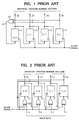
- Such artificial random-number pattern generator is formed, for example, as shown in Figs. 1 and 2, by a plurality of flip-flops 11 - 14 each having a clock signal input terminal, and an exclusive OR gate 30 for receiving outputs from at least two flip-flops out of the plurality of flop-flops.
- Such artificial random-number pattern generator is disclosed in "Logic Design Principles", 1986, Prentice-Hall, Pages 458 and 469, U.S.A.
- the conventional random-number pattern generators as described above only have a function of generating artificial random-number patterns and can make a diagnosis of failure only in the internal circuit of the LSI.
- a disadvantage in such conventional generators is that it is not possible to conduct overall tests including those for input and output buffer circuits of the mounted LSI chip on a board or those for external wirings of the LSI.
- US-A-4 860 236 discloses a multiple bit artificial random-number pattern generator comprising N flip-flops, where N is greater than or equal to two, each of the first to N-th flip-flops having an input terminal, a set signal input terminal and a clock signal input terminal; (N-1) selectors, each of which receives an output from the (1+i)th (1 ⁇ i ⁇ (N-1)) flip-flop and an i-th input data and selectively forwards its output to the input terminal of the i-th flip-flop; an artificial random-number producing means which receives outputs from at least two of said N flip-flops, conducts a predetermined logical operation on said outputs, and outputs an artificial random-number data of 1 bit; and an N-th selector which receives the output data from said artificial random-number producing means, and an external output data, and which selectively forwards its output to the input terminal of said N-th flip-flop; each of said plurality of (N-1) selectors being supplied
- the present invention provides a multiple bit artificial random-number pattern generator as defined in independent claims 1 and/or 3 to which reference should now be made. Preferred features of embodiments of the invention are listed in the dependent claims.
- the artificial random-number pattern generator in order to generate artificial random-number patterns of N-bits, is provided with flip-flops and selectors constituted by N+1 number of the basic circuits which are repetition of substantially the same circuit.
- selectors To the particular one (1) added selector are inputted an output of the exclusive OR gate and an external output data so that, by causing one of them to be outputted therefrom according to the operation mode signal, it is possible to arrange the artificial random-number generator by simple repetition by the number N+1 of the same flip-flops and the same two-input selectors.
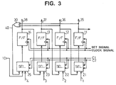
- Fig.3 is a circuit diagram showing an artificial random-number pattern generator capable of operating as a random-number generator, a boundary scanning buffer and an input buffer.
- a table 1 shows the operation of the artificial random-number pattern generator shown in Fig. 3.
- the artificial random-number pattern generator shown in Fig. 3 operates in three different ways in accordance with the combinations of the first operation mode signal C1 and the second operation mode signal C2 which are commonly supplied to the selectors 21 - 23 and 25.
- the selectors 21 - 23 forward to the corresponding flip-flops 11 - 13 the corresponding input data 1 - 3, respectively.
- the selector 25 forwards to the flip-flop 14 the input data 4.
- Each of the flip-flops 11 - 14 outputs the input data 1 - 4 as it is with a delay of one clock signal.
- the artificial random-number pattern generator operates as an input or output buffer.
- each of the selectors 21 - 23 selectively forwards an output 36 - 38 of the corresponding following flip-flop 12 - 14 to each of the flip-flops 11 - 13.
- the selector 25 forwards to the flip-flop 14 the external output 10 supplied from the external flip-flop.
- Each of the flip-flops 11 - 14 outputs the supplied data as it is with a delay of one clock signal, so that the overall circuit of this invention operates as a boundary scanning buffer.
- each of the selectors 21 - 23 selectively forwards to each of the flip-flops 11 - 13 a corresponding exclusive logical OR of the output data 36, 37, 38 and the input data 1 - 3.
- the selector 25 forwards to the flip-flop 14 an exclusive logical OR of the output data 40 of the exclusive OR gate 30 and the input data 4.
- Each of the flip-flops 11 - 14 accordingly outputs the supplied data as it is with a delay of one clock signal, so that the overall circuit of this invention operates as an artificial random-number pattern generator.
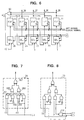
- Fig. 4 is a circuit diagram showing an artificial random-number pattern generator of an embodiment according to the present invention.
- Fig. 5 shows a detailed circuit diagram of the 3-input selector 27 shown in Fig. 4.
- the selector 27 includes two 3-input AND gates 271, 272, a 2-input AND gate 273, a 3-input OR gate 274 and two inverters 275, 276.
- the selector 27 selectively outputs one of the external output 10, the output 40 of the exclusive OR gate 30 and the input data 4 in accordance with the combinations of the first and second operation mode signals C1 and C2.
- the table 2 shows the operation of the artificial random-number pattern generator shown in Fig. 4.
- the artificial random-number pattern generator shown in Fig. 4 operates in three different ways in accordance with the combinations of the first operation mode signal C1 and the second operation mode signal C2.
- each of the flip-flops 11 - 13 receives an output of the corresponding preceding flip-flop 12 - 14 and outputs it as it is with a delay of one clock signal, whereas the flip-flop 14 outputs a signal in the value of the output 40 of the exclusive OR gate 30, so that the overall circuit operates as an artificial random-number pattern generator.
- each of the flip-flops 11 - 13 receives an output of the corresponding preceding flip-flop 12 - 14 and outputs it as it is with a delay of one clock signal, whereas the flip-flop 14 outputs a signal in the value of the output 10 of the adjacent flip-flop, so that the overall circuit operates as a boundary scanning buffer which forms a part of the boundary scanning path.
- each of the flip-flops 11 - 14 outputs the input data 1 - 4 as it is, so that the overall circuit operates as an input buffer.
- Fig. 6 is a circuit diagram showing an artificial random-number pattern generator not falling within the scope of the present invention as claimed.
- Fig. 7 shows a detailed circuit diagram of the selector 26 in Fig. 6.
- the selector 26 is formed by, for example, four 2-input AND gates 261 - 264, two 2-input OR gates 265, 266, a 2-input exclusive OR gate 267 and two inverters 268, 269.
- Fig. 8 shows a detailed circuit diagram of the selector 23 in Fig. 6.
- the selector 23 has a NAND gate 231 which receives both the first and second operation mode signals C1, C2, in addition to the same circuit as the selector 26 shown in Fig. 7.
- Each of the remaining selectors 21, 22 and 24 has the same circuit configuration as that of the selector 23 explained above.
- a table 3 shows the operation of the artificial random-number pattern generator shown in Fig. 6.
- the artificial random-number pattern generator shown in Fig. 6 operates in three different ways in accordance with the combinations of the first operation mode signal C1 and the second operation mode signal C2.
- the selectors 21 - 24 forward to the corresponding flip-flops 11 - 14 the corresponding input data 1 - 4, respectively.
- Each of the flip-flops 11 - 14 thus outputs the input data 1 - 4 as it is.
- the artificial random-number pattern generator as a whole operates as an input or output buffer.
- each of the selectors 21 - 24 selectively forwards an output 36 - 39 of the corresponding preceding flip-flop 12 - 15 to each of the flip-flops 11 - 14.
- the selector 26 forwards to the flip-flop 15 the output 10 supplied from the external flip-flop.
- Each of the flip-flops 11 - 14 outputs the supplied data as it is with a delay of one clock signal, so that the overall circuit of this invention operates as a boundary scanning buffer.
- each of the selectors 21 - 24 selectively forwards to each of the flip-flops 11 - 14 a corresponding exclusive logical OR of the output data 36, 37, 38, 39 and the input data 1, 2, 3, 4.
- the selector 26 forwards to the flip-flop 15 the output data 40 of the exclusive OR gate 30.
- Each of the flip-flops 11 - 14 accordingly outputs the supplied data at it is with a delay of one clock signal, so that the overall circuit of this invention operates as the same artificial random-number pattern generator as the conventional one.
- Fig. 9 is a circuit diagram showing an artificial random-number pattern generator of another embodiment according to the present invention.
- the table 4 shows the operation of the artificial random-number pattern generator shown in Fig. 9.
- OUTPUT DATA 40 FROM EX-OR 30 INPUT BUFFER 1 0 OUTPUT OF FLIP-FLOP f+1
- the artificial random-number pattern generator of the embodiment shown in Fig. 9 operates in three different ways in accordance with the combinations of the first operation mode signal C1 and the second operation mode signal C2.
- the input data 1 - 4 are outputted as they are irrespective of the value of the output of the flip-flop 15, that is, irrespective of the value of the second operation mode signal C2, so that the pattern generator operates as an input buffer.
- the pattern generator operates as a boundary scanning buffer.
Landscapes
- Engineering & Computer Science (AREA)
- General Engineering & Computer Science (AREA)
- Physics & Mathematics (AREA)
- General Physics & Mathematics (AREA)
- Theoretical Computer Science (AREA)
- Mathematical Optimization (AREA)
- Mathematical Analysis (AREA)
- Pure & Applied Mathematics (AREA)
- Computational Mathematics (AREA)
- Computer Hardware Design (AREA)
- Quality & Reliability (AREA)
- Tests Of Electronic Circuits (AREA)
- Test And Diagnosis Of Digital Computers (AREA)
Claims (4)
- Générateur de configurations de nombres aléatoires artificiels à N bits comprenant :dans lequel :une pluralité de N bascules (11 à 14), une première à une N-ième, avec N ≥ 2, chacune ayant une borne d'entrée, une borne d'entrée de signal de mise à un et une borne d'entrée de signal d'horloge ;une pluralité de (N - 1) sélecteurs (21 à 23), un premier à un (N - 1)-ième, chacun recevant une sortie de ladite (1 + i)-ième bascule, avec 1 ≤ i ≤ N - 1, et des i-ièmes données d'entrée (1, 2, 3) et envoyant de façon sélective sa sortie à ladite borne d'entrée desdites i-ièmes bascules ;des moyens de génération de nombres aléatoires artificiels (30) qui reçoivent des sorties (35, 36) provenant d'au moins deux (11, 12) desdites N bascules, exécutent une opération logique prédéterminée sur lesdites sorties, et sortent des données de nombres aléatoires artificiels (40) d'1 bit ; etun N-ième sélecteur (25 ; 27) qui reçoit les données de sortie (40) provenant desdits moyens de génération de nombres aléatoires artificiels, des données de sortie externes (10), et des N-ièmes données d'entrée (4), et qui envoie de façon sélective sa sortie à la borne d'entrée de ladite N-ième bascule (14) ;chacun de ladite pluralité de (N - 1) sélecteurs (21 à 23) est fourni avec un premier signal de mode de fonctionnement (C1), et envoie de façon sélective à ladite borne d'entrée de ladite i-ième bascule soit ladite sortie de ladite (1 + i)-ième bascule, soit lesdites i-ièmes données d'entrée (1, 2, 3) selon ledit premier signal de mode de fonctionnement (C1) ; etledit N-ième sélecteur (27) est fourni avec ledit premier signal de mode de fonctionnement (C1) et avec un second signal de mode de fonctionnement (C2) et envoie de façon sélective à la borne d'entrée de ladite N-ième bascule (14) soit lesdites données de sortie (40) provenant desdits moyens de génération de nombres aléatoires artificiels (30), soit lesdites données de sortie externes (10), soit encore lesdites N-ièmes données d'entrée (4) selon lesdits premier et second signaux de mode de fonctionnement (C1, C2),ce par quoi ledit générateur de configurations de nombres aléatoires artificiels fonctionne soit comme un générateur de configurations de nombres aléatoires artificiels, soit comme un tampon de balayage de limite, soit comme un tampon d'entrée selon les combinaisons desdits premier et second signaux de mode de fonctionnement.
- Générateur de configurations de nombres aléatoires artificiels à N bits selon la revendication 1, dans lequel lesdits moyens de génération de nombres aléatoires artificiels sont une porte OU exclusif (30) qui exécute une opération de OU logique exclusif d'au moins deux sorties (35, 36) provenant de ladite pluralité de N bascules (11 à 14).
- Générateur de configurations de nombres aléatoires artificiels à N bits comprenant :et dans lequel :une pluralité de (N + 1) bascules (11 à 15), une première à une (N + 1)-ième, avec N ≥ 2, chacune ayant une borne d'entrée, une borne d'entrée de signal de mise à un et une borne d'entrée de signal d'horloge ;une pluralité de N sélecteurs (21 à 24), un premier à un N-ième, chacun recevant une sortie de ladite (1 + i)-ième bascule, avec 1 ≤ i ≤ N, et des i-ièmes données d'entrée (1, 2, 3, 4) et envoyant de façon sélective sa sortie à ladite borne d'entrée de ladite i-ième bascule ;des moyens de génération de nombres aléatoires artificiels (30) qui reçoivent des sorties (35, 36) provenant d'au moins deux (11, 12) desdites (N + 1) bascules (11 à 15), exécutent une opération logique prédéterminée sur lesdites sorties, et sortent des données de nombres aléatoires artificiels (40) d'1 bit ; etun (N + 1)-ième sélecteur (26, 28) qui reçoit les données de sortie (40) provenant desdits moyens de génération de nombres aléatoires artificiels (30) et des données de sortie externes (10), et qui envoie de façon sélective à la borne d'entrée de ladite (N + 1)-ième bascule soit lesdites données de sortie (40) provenant desdits moyens de génération de nombres aléatoires artificiels (30), soit lesdites données de sortie externes (10)chacun de ladite pluralité de N sélecteurs (21 à 24) est fourni avec un premier signal de mode de fonctionnement (C1), et envoie de façon sélective à ladite borne d'entrée de ladite i-ième bascule soit ladite sortie (36, 37, 38, 39) de ladite (1 + i)-ième bascule (12, 13, 14, 15), soit lesdites i-ièmes données d'entrée (1, 2, 3, 4) selon ledit premier signal de mode de fonctionnement (C1) ; etledit (N + 1)-ième sélecteur (28) est fourni avec un second signal de mode de fonctionnement (C2) et envoie de façon sélective à la borne d'entrée de ladite (N + 1)-ième bascule (15) soit lesdites données de sortie (40) provenant desdits moyens de génération de nombres aléatoires artificiels (30), soit lesdites données de sortie externes (10) selon ledit second signal de mode de fonctionnement (C2),ce par quoi ledit générateur de configurations de nombres aléatoires artificiels fonctionne soit comme un circuit de génération de configurations de nombres aléatoires artificiels, soit comme un tampon de balayage de limite, soit encore comme un tampon d'entrée selon les combinaisons desdits premier et second signaux de mode de fonctionnement.
- Générateur de configurations de nombres aléatoires artificiels à N bits selon la revendication 3, dans lequel lesdits moyens de génération de nombres aléatoires artificiels sont une porte OU exclusif (30) qui exécute une opération de OU logique exclusif d'au moins deux sorties (35, 36) provenant de ladite pluralité de (N + 1) bascules (11 à 15).
Priority Applications (1)
| Application Number | Priority Date | Filing Date | Title |
|---|---|---|---|
| EP98200796A EP0853276A3 (fr) | 1991-02-04 | 1992-01-10 | Circuit de génération de configurations de nombres aléatoires artificiels |
Applications Claiming Priority (3)
| Application Number | Priority Date | Filing Date | Title |
|---|---|---|---|
| JP13372/91 | 1991-02-04 | ||
| JP3013372A JP2841882B2 (ja) | 1991-02-04 | 1991-02-04 | 疑似乱数パタン発生器 |
| JP1337291 | 1991-02-04 |
Related Child Applications (1)
| Application Number | Title | Priority Date | Filing Date |
|---|---|---|---|
| EP98200796A Division EP0853276A3 (fr) | 1991-02-04 | 1992-01-10 | Circuit de génération de configurations de nombres aléatoires artificiels |
Publications (2)
| Publication Number | Publication Date |
|---|---|
| EP0498534A1 EP0498534A1 (fr) | 1992-08-12 |
| EP0498534B1 true EP0498534B1 (fr) | 1999-06-09 |
Family
ID=11831261
Family Applications (2)
| Application Number | Title | Priority Date | Filing Date |
|---|---|---|---|
| EP98200796A Withdrawn EP0853276A3 (fr) | 1991-02-04 | 1992-01-10 | Circuit de génération de configurations de nombres aléatoires artificiels |
| EP92300256A Expired - Lifetime EP0498534B1 (fr) | 1991-02-04 | 1992-01-10 | Circuit de génération de configurations de nombres aléatoires artificiels |
Family Applications Before (1)
| Application Number | Title | Priority Date | Filing Date |
|---|---|---|---|
| EP98200796A Withdrawn EP0853276A3 (fr) | 1991-02-04 | 1992-01-10 | Circuit de génération de configurations de nombres aléatoires artificiels |
Country Status (4)
| Country | Link |
|---|---|
| US (1) | US5331581A (fr) |
| EP (2) | EP0853276A3 (fr) |
| JP (1) | JP2841882B2 (fr) |
| DE (1) | DE69229362T2 (fr) |
Cited By (1)
| Publication number | Priority date | Publication date | Assignee | Title |
|---|---|---|---|---|
| RU2250489C1 (ru) * | 2003-07-01 | 2005-04-20 | Военный университет связи | Генератор случайной последовательности |
Families Citing this family (12)
| Publication number | Priority date | Publication date | Assignee | Title |
|---|---|---|---|---|
| GB9303758D0 (en) * | 1993-02-25 | 1993-04-14 | Texas Instruments Ltd | Improvements in or relating to integrated logic circuits |
| JP2845308B2 (ja) * | 1993-04-02 | 1999-01-13 | 株式会社アドバンテスト | 並列疑似ランダムパターン発生器 |
| JPH07154214A (ja) * | 1993-11-26 | 1995-06-16 | Nec Corp | ディジタル信号処理回路 |
| US5574673A (en) * | 1993-11-29 | 1996-11-12 | Board Of Regents, The University Of Texas System | Parallel architecture for generating pseudo-random sequences |
| KR100657240B1 (ko) * | 1999-07-10 | 2007-01-12 | 삼성전자주식회사 | 랜덤 데이터 발생기 |
| US6631390B1 (en) | 2000-03-06 | 2003-10-07 | Koninklijke Philips Electronics N.V. | Method and apparatus for generating random numbers using flip-flop meta-stability |
| US6629116B1 (en) * | 2000-05-05 | 2003-09-30 | Koninklijke Philips Electronics N.V. | Random sequence generators |
| US6943668B2 (en) | 2001-06-26 | 2005-09-13 | General Electric Company | Apparatus and method for reconfiguring a power line communication system |
| US20030014451A1 (en) * | 2001-07-12 | 2003-01-16 | Optix Networks Inc. | Method and machine for scrambling parallel data channels |
| RU2211481C2 (ru) * | 2001-10-08 | 2003-08-27 | Военный университет связи | Генератор случайных чисел |
| JP2006072891A (ja) * | 2004-09-06 | 2006-03-16 | Sony Corp | セルオートマトンに基づく、制御可能な周期を有する擬似乱数シーケンスの生成方法および装置 |
| CN101533069B (zh) * | 2009-04-03 | 2011-04-06 | 西安交通大学 | 集成电路的复合扫描单元 |
Family Cites Families (7)
| Publication number | Priority date | Publication date | Assignee | Title |
|---|---|---|---|---|
| US3875377A (en) * | 1972-12-29 | 1975-04-01 | Alsthom Cgee | Noise generator |
| US4377757A (en) * | 1980-02-11 | 1983-03-22 | Siemens Aktiengesellschaft | Logic module for integrated digital circuits |
| US4680539A (en) * | 1983-12-30 | 1987-07-14 | International Business Machines Corp. | General linear shift register |
| US4785410A (en) * | 1985-06-05 | 1988-11-15 | Clarion Co., Ltd. | Maximum length shift register sequences generator |
| US4860236A (en) * | 1987-10-26 | 1989-08-22 | University Of Manitoba | Cellular automaton for generating random data |
| US4894800A (en) * | 1988-09-23 | 1990-01-16 | Honeywell, Inc. | Reconfigurable register bit-slice for self-test |
| US5105376A (en) * | 1990-08-08 | 1992-04-14 | Vlsi Technology, Inc. | Linear feedback shift registers |
-
1991
- 1991-02-04 JP JP3013372A patent/JP2841882B2/ja not_active Expired - Lifetime
-
1992
- 1992-01-10 EP EP98200796A patent/EP0853276A3/fr not_active Withdrawn
- 1992-01-10 EP EP92300256A patent/EP0498534B1/fr not_active Expired - Lifetime
- 1992-01-10 DE DE69229362T patent/DE69229362T2/de not_active Expired - Fee Related
- 1992-01-10 US US07/818,757 patent/US5331581A/en not_active Expired - Fee Related
Cited By (1)
| Publication number | Priority date | Publication date | Assignee | Title |
|---|---|---|---|---|
| RU2250489C1 (ru) * | 2003-07-01 | 2005-04-20 | Военный университет связи | Генератор случайной последовательности |
Also Published As
| Publication number | Publication date |
|---|---|
| DE69229362T2 (de) | 2000-03-02 |
| EP0853276A3 (fr) | 1998-08-05 |
| US5331581A (en) | 1994-07-19 |
| EP0498534A1 (fr) | 1992-08-12 |
| JP2841882B2 (ja) | 1998-12-24 |
| JPH04313119A (ja) | 1992-11-05 |
| EP0853276A2 (fr) | 1998-07-15 |
| DE69229362D1 (de) | 1999-07-15 |
Similar Documents
| Publication | Publication Date | Title |
|---|---|---|
| US4635261A (en) | On chip test system for configurable gate arrays | |
| US5268949A (en) | Circuit for generating M-sequence pseudo-random pattern | |
| EP0498534B1 (fr) | Circuit de génération de configurations de nombres aléatoires artificiels | |
| US4740970A (en) | Integrated circuit arrangement | |
| US6968486B2 (en) | Master-slave-type scanning flip-flop circuit for high-speed operation with reduced load capacity of clock controller | |
| US6466049B1 (en) | Clock enable control circuit for flip flops | |
| US4862068A (en) | LSI logic circuit | |
| JP3183260B2 (ja) | スキャンフリップフロップ回路 | |
| JPH07167921A (ja) | バウンダリスキャンセル装置とバウンダリスキャンテスト方法 | |
| US5719913A (en) | Pseudo-random number generating circuit and bidirectional shift register | |
| JP2632731B2 (ja) | 集積回路装置 | |
| GB2030807A (en) | Latch circuit | |
| US5337321A (en) | Scan path circuit with clock signal feedback, for skew avoidance | |
| US4775810A (en) | Parity check logic circuit | |
| JPS63158475A (ja) | スキヤンパス方式の論理集積回路 | |
| KR100326908B1 (ko) | 반도체 집적회로 | |
| KR100413763B1 (ko) | 탭드 코아 선택회로를 구비하는 반도체 집적회로 | |
| US4249246A (en) | Programmable logic array for generating EOR sums of input signals | |
| US5321641A (en) | Pseudo random pattern generation circuit | |
| US5465257A (en) | Test signal output circuit in LSI | |
| US20040095166A1 (en) | Clock switching circuit | |
| IE80388B1 (en) | Circuit arrangement for testing integrated circuits | |
| US4894800A (en) | Reconfigurable register bit-slice for self-test | |
| JPH0440736B2 (fr) | ||
| GB2175097A (en) | Testing digital integrated circuits |
Legal Events
| Date | Code | Title | Description |
|---|---|---|---|
| PUAI | Public reference made under article 153(3) epc to a published international application that has entered the european phase |
Free format text: ORIGINAL CODE: 0009012 |
|
| 17P | Request for examination filed |
Effective date: 19920131 |
|
| AK | Designated contracting states |
Kind code of ref document: A1 Designated state(s): DE FR GB |
|
| 17Q | First examination report despatched |
Effective date: 19961029 |
|
| GRAG | Despatch of communication of intention to grant |
Free format text: ORIGINAL CODE: EPIDOS AGRA |
|
| GRAG | Despatch of communication of intention to grant |
Free format text: ORIGINAL CODE: EPIDOS AGRA |
|
| GRAG | Despatch of communication of intention to grant |
Free format text: ORIGINAL CODE: EPIDOS AGRA |
|
| GRAH | Despatch of communication of intention to grant a patent |
Free format text: ORIGINAL CODE: EPIDOS IGRA |
|
| GRAH | Despatch of communication of intention to grant a patent |
Free format text: ORIGINAL CODE: EPIDOS IGRA |
|
| GRAA | (expected) grant |
Free format text: ORIGINAL CODE: 0009210 |
|
| AK | Designated contracting states |
Kind code of ref document: B1 Designated state(s): DE FR GB |
|
| REF | Corresponds to: |
Ref document number: 69229362 Country of ref document: DE Date of ref document: 19990715 |
|
| ET | Fr: translation filed | ||
| PLBE | No opposition filed within time limit |
Free format text: ORIGINAL CODE: 0009261 |
|
| 26N | No opposition filed | ||
| REG | Reference to a national code |
Ref country code: GB Ref legal event code: IF02 |
|
| PGFP | Annual fee paid to national office [announced via postgrant information from national office to epo] |
Ref country code: DE Payment date: 20020130 Year of fee payment: 11 |
|
| PGFP | Annual fee paid to national office [announced via postgrant information from national office to epo] |
Ref country code: GB Payment date: 20030108 Year of fee payment: 12 |
|
| PGFP | Annual fee paid to national office [announced via postgrant information from national office to epo] |
Ref country code: FR Payment date: 20030127 Year of fee payment: 12 |
|
| PG25 | Lapsed in a contracting state [announced via postgrant information from national office to epo] |
Ref country code: DE Free format text: LAPSE BECAUSE OF NON-PAYMENT OF DUE FEES Effective date: 20030801 |
|
| PG25 | Lapsed in a contracting state [announced via postgrant information from national office to epo] |
Ref country code: GB Free format text: LAPSE BECAUSE OF NON-PAYMENT OF DUE FEES Effective date: 20040110 |
|
| GBPC | Gb: european patent ceased through non-payment of renewal fee |
Effective date: 20040110 |
|
| PG25 | Lapsed in a contracting state [announced via postgrant information from national office to epo] |
Ref country code: FR Free format text: LAPSE BECAUSE OF NON-PAYMENT OF DUE FEES Effective date: 20040930 |
|
| REG | Reference to a national code |
Ref country code: FR Ref legal event code: ST |