EP0498574A2 - Einrichtung zur Wellenformentzerrung mit neuronalem Netzwerk und Verfahren zum Entwurf derselben - Google Patents
Einrichtung zur Wellenformentzerrung mit neuronalem Netzwerk und Verfahren zum Entwurf derselben Download PDFInfo
- Publication number
- EP0498574A2 EP0498574A2 EP92300838A EP92300838A EP0498574A2 EP 0498574 A2 EP0498574 A2 EP 0498574A2 EP 92300838 A EP92300838 A EP 92300838A EP 92300838 A EP92300838 A EP 92300838A EP 0498574 A2 EP0498574 A2 EP 0498574A2
- Authority
- EP
- European Patent Office
- Prior art keywords
- values
- neural network
- signal
- learning
- input
- Prior art date
- Legal status (The legal status is an assumption and is not a legal conclusion. Google has not performed a legal analysis and makes no representation as to the accuracy of the status listed.)
- Granted
Links
Images





Classifications
-
- G—PHYSICS
- G11—INFORMATION STORAGE
- G11B—INFORMATION STORAGE BASED ON RELATIVE MOVEMENT BETWEEN RECORD CARRIER AND TRANSDUCER
- G11B20/00—Signal processing not specific to the method of recording or reproducing; Circuits therefor
- G11B20/10—Digital recording or reproducing
- G11B20/10009—Improvement or modification of read or write signals
- G11B20/10481—Improvement or modification of read or write signals optimisation methods
- G11B20/10518—Improvement or modification of read or write signals optimisation methods using neural networks
-
- G—PHYSICS
- G06—COMPUTING OR CALCULATING; COUNTING
- G06N—COMPUTING ARRANGEMENTS BASED ON SPECIFIC COMPUTATIONAL MODELS
- G06N3/00—Computing arrangements based on biological models
- G06N3/02—Neural networks
- G06N3/06—Physical realisation, i.e. hardware implementation of neural networks, neurons or parts of neurons
- G06N3/063—Physical realisation, i.e. hardware implementation of neural networks, neurons or parts of neurons using electronic means
-
- G—PHYSICS
- G11—INFORMATION STORAGE
- G11B—INFORMATION STORAGE BASED ON RELATIVE MOVEMENT BETWEEN RECORD CARRIER AND TRANSDUCER
- G11B20/00—Signal processing not specific to the method of recording or reproducing; Circuits therefor
- G11B20/10—Digital recording or reproducing
- G11B20/10009—Improvement or modification of read or write signals
-
- G—PHYSICS
- G11—INFORMATION STORAGE
- G11B—INFORMATION STORAGE BASED ON RELATIVE MOVEMENT BETWEEN RECORD CARRIER AND TRANSDUCER
- G11B20/00—Signal processing not specific to the method of recording or reproducing; Circuits therefor
- G11B20/22—Signal processing not specific to the method of recording or reproducing; Circuits therefor for reducing distortions
-
- G—PHYSICS
- G11—INFORMATION STORAGE
- G11B—INFORMATION STORAGE BASED ON RELATIVE MOVEMENT BETWEEN RECORD CARRIER AND TRANSDUCER
- G11B5/00—Recording by magnetisation or demagnetisation of a record carrier; Reproducing by magnetic means; Record carriers therefor
- G11B5/02—Recording, reproducing, or erasing methods; Read, write or erase circuits therefor
- G11B5/027—Analogue recording
- G11B5/035—Equalising
-
- G—PHYSICS
- G11—INFORMATION STORAGE
- G11B—INFORMATION STORAGE BASED ON RELATIVE MOVEMENT BETWEEN RECORD CARRIER AND TRANSDUCER
- G11B5/00—Recording by magnetisation or demagnetisation of a record carrier; Reproducing by magnetic means; Record carriers therefor
- G11B5/02—Recording, reproducing, or erasing methods; Read, write or erase circuits therefor
- G11B5/09—Digital recording
-
- G—PHYSICS
- G11—INFORMATION STORAGE
- G11B—INFORMATION STORAGE BASED ON RELATIVE MOVEMENT BETWEEN RECORD CARRIER AND TRANSDUCER
- G11B7/00—Recording or reproducing by optical means, e.g. recording using a thermal beam of optical radiation by modifying optical properties or the physical structure, reproducing using an optical beam at lower power by sensing optical properties; Record carriers therefor
- G11B7/004—Recording, reproducing or erasing methods; Read, write or erase circuits therefor
-
- H—ELECTRICITY
- H04—ELECTRIC COMMUNICATION TECHNIQUE
- H04L—TRANSMISSION OF DIGITAL INFORMATION, e.g. TELEGRAPHIC COMMUNICATION
- H04L25/00—Baseband systems
- H04L25/02—Details ; arrangements for supplying electrical power along data transmission lines
- H04L25/03—Shaping networks in transmitter or receiver, e.g. adaptive shaping networks
- H04L25/03006—Arrangements for removing intersymbol interference
- H04L25/03165—Arrangements for removing intersymbol interference using neural networks
-
- H—ELECTRICITY
- H04—ELECTRIC COMMUNICATION TECHNIQUE
- H04L—TRANSMISSION OF DIGITAL INFORMATION, e.g. TELEGRAPHIC COMMUNICATION
- H04L25/00—Baseband systems
- H04L25/02—Details ; arrangements for supplying electrical power along data transmission lines
- H04L25/03—Shaping networks in transmitter or receiver, e.g. adaptive shaping networks
- H04L25/03006—Arrangements for removing intersymbol interference
- H04L2025/03433—Arrangements for removing intersymbol interference characterised by equaliser structure
- H04L2025/03439—Fixed structures
- H04L2025/03445—Time domain
- H04L2025/03464—Neural networks
-
- Y—GENERAL TAGGING OF NEW TECHNOLOGICAL DEVELOPMENTS; GENERAL TAGGING OF CROSS-SECTIONAL TECHNOLOGIES SPANNING OVER SEVERAL SECTIONS OF THE IPC; TECHNICAL SUBJECTS COVERED BY FORMER USPC CROSS-REFERENCE ART COLLECTIONS [XRACs] AND DIGESTS
- Y10—TECHNICAL SUBJECTS COVERED BY FORMER USPC
- Y10S—TECHNICAL SUBJECTS COVERED BY FORMER USPC CROSS-REFERENCE ART COLLECTIONS [XRACs] AND DIGESTS
- Y10S706/00—Data processing: artificial intelligence
- Y10S706/902—Application using ai with detail of the ai system
- Y10S706/903—Control
- Y10S706/909—Communication
Definitions
- the present invention relates to a waveform equalizer for removing signal distortion which arises when a digital signal is recorded and subsequently reproduced, or is transmitted and subsequently received, and to a method of designing such a waveform equalizer.
- the invention relates to a waveform equalizer which is formed as a neural network having fixed weighting coefficients.
- digital signal transfer system as used in the following description and in the appended claims is intended to designate a system such as a magnetic or optical recording and playback system,or a digital signal transmission system, in which an original signal is recorded and reproduced to obtain a corresponding distorted digital signal, or is transmitted and received, to obtain a corresponding distorted digital signal.
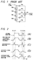
- a type of waveform equalizer has been used in the prior art which is based on a transversal filter, as illustrated in the circuit diagram of Fig. 1.
- the waveform equalizer is assumed to receive as input signal a distorted digital signal produced from a recording and playback system.
- the output signal from the playback apparatus is delayed by successive identical amounts in delay lines 130a to 130d respectively.
- the directly supplied input signal and the lines input signal outputs produced from the delay lines are amplified by amplifiers 131a to 131d respectively, which have predetermined respectively different amplification factors.
- the resultant amplified output signals are then summed by the adder circuit 132, to obtain a waveform-equalized output signal.
- Such a waveform equalizer apparatus does not provide satisfactory results.
- Diagrams (A) to (E) of Fig. 2 are waveform diagrams for illustrating how such distortion occurs in a magnetic recording and playback system. It is assumed here that NRZ (Non Return to Zero) code is recorded and played back, and that the original recording current signal has an ideal digital waveform, i.e. with rapid transitions between fixed 0 and 1 state digital levels as illustrated in diagram (A). However the magnetic pattern that is actually recorded will be of the form shown in diagram (B).
- NRZ Non Return to Zero
- the playback signal that is actually obtained in this case will be substantially distorted.
- an amount of peak shift such as the amount ⁇ t has occurred in the differentiated waveform, as shown in diagram (E).
- a peak value in the differentiated playback signal which should correspond to a recording signal level transition at point t2 of the original recording signal has been displaced. That is to say, for some portions of the playback signal waveform, peak values of the differentiated playback signal will be time-displaced from the correct positions of these peak values.
- one bit is represented by a magnetic polarity inversion.
- Diagrams (A) to (D) of Fig 3 illustrate how signal distortion can arise in an optical recording and playback system.
- Tmin designates a minimum duration for which the recorded data remains continuously at the digital 1 or 0 state.
- the data that are actually recorded or the disk i.e. as elongated surface pits, of varying length
- channel bits which are synchronized with a clock signal known as the channel clock signal, having a frequency of approximately 4.32 MHz.
- the period of that channel clock signal is commonly referred to simply as T, and that designation will be used in the following.
- Tmin The minum interval between successive inversions of that recorded data will be designated as Tmin.
- the value of Tmin is three periods of the channel clock signal, i.e 3 T, as illustrated by Fig. 4.
- CDs may be utilized in which the recorded data has a value of Tmin that is less than 3 T.
- t1, t2, t3 and t4 denote respective time points which are defined by a the aforementioned channel clock signal.
- the data inversion joint X in the original data which occurs at a time point t2 is preceded by 1 Tmin period at the digital 0 state, and succeeded by 3 Tmin periods at the digital 1 state.
- the data inversion point Y is preceded by 3 Tmin periods at the digital 1 state and is succeeded by one Tmin period at the digital 0 state.
- Playback of an optical disk is based upon energy, and such playback operation does not include elements which ire of mutually opposite kind, such as the N and S polarities of a magnetic recording and playback system. For that reason, when a lack of sharpness due to spherical aberration in the optical system arises, then as shown in diagram (B) of Fig 3, the ends of the long code portion (3Tmin of data) will become lengthened so that the portion of the waveform at time point t2 is shifted towards the time point t1 and the portion of the waveform at t3 is shifted towards t4. In addition, the distortion that results from coma aberration can cause even more serious effects.
- Diagram (C) of Fig 3 shows a case in which coma aberration is produced which is oriented in the opposite direction to the direction of disk rotation
- diagram (D) shows a case in which coma aberration is produced which is oriented along the direction of disk rotation. It can be seen that the amount and shape of the waveform distortion of the playback signal will differ in accordance with these two types of coma aberration.
- a neural network consists of a plurality of neuron units, each having a non-linear input/output characteristic, and interconnected by linking elements which have respective mutually independent weighting coefficients.
- the weighting coefficients can be altered by a learning operation, which involves comparing an output value produced from the neural network (while a specific combination of input values are being inputted to the neural network) with a desired value (referred to as a teaching value), and modifying the values of the weighting coefficients such as to bring the output value from the neural network closer to the teaching value, by using a learning algorithm.
- the learning process is successively repeated for a number of different teaching values and corresponding input value combinations.
- a neural network is generally implemented by simulation using a computer.
- a neural network due to the limited processing speed capabilities of the usual types of computer
- real-time signal processing for such a waveform equalizer type of application.
- a waveform equalizer is configured as a neural network circuit formed of a plurality of circuit units functioning as neuron units each having a non-linear input/output characteristic, which are interconnected by linking elements having fixed, respectively independently established weighting coefficients.
- These weighting coefficients are established beforehand by generating a simulated neural network having variable weighting coefficients, whose configuration is equivalent to that of the waveform equalizer neural network, by means of a suitably programmed computer. While inputting successive values of a distorted digital signal to the simulated neural network and comparing the resultant output values produced from that simulated neural network with desired (i.e.
- the weighting coefficients of the simulated neural network are successively varied until suitable values are obtained, by using a known type of learning algorithm such as a back-propogation algorithm which operates on the basis of results obtained from the aforementioned comparisons.
- the weighting coefficients which are obtained as final values are then used to determine respective values for the corresponding fixed weighting coefficients for the neural network of the actual waveform equalizer circuit, for example to determine the respective values of resistors which are used as linking elements providing fixed weighting coefficients.
- the learning function and the actual signal processing function can be optimally executed mutually separately, enabling a waveform equalizer to be provided wich performs effective real-time equalization of a distorted digital signal produced from a playback system or transmission system.
- the finally obtained waveform equalizer (formed as a neural network, with fixed weighting coefficients) can be implemented by a hardware circuit configuration that is based on generally available types of analog components such as operational amplifiers, diodes and resistors.
- the learning function is of course unnecessary, so that the waveform equalizer configuration can be simple, and high-speed processing can be achieved.
- the present invention provides a waveform equalizer for processing an input distorted digital signal, comprising: delay means coupled to receive the input distorted digital signal, for delaying the distorted digital signal by successive fixed amounts to obtain a plurality of delayed distorted digital signals; and a plurality of neuron units, and a plurality of linking elements having respectively fixed weighting coefficients, the linking elements interconnecting the neuron units to form a neural network which is coupled to receive the input distorted digital signal and delayed distorted digital signals as input signals thereto, and which produces a waveform-equalized output digital signal in response to the input signals.
- Respective values for the fixed weighting coefficients are established by a learning procedure employing a computer-simulated neural network having variable weighting coefficients and having a network configuration corresponding to that of the neural network of the waveform equalizer.
- the learning operation includes supplying to the computer-simulated neural network an input distorted digital signal while comparing with an output signal obtained from that neural network a teaching signal which is an undistorted digital signal corresponding to the distorted digital signal, and applying a predetermined learning algorithm to alter the variable weighting coefficients in accordance with differences between the teaching signal and the neural network output signal.
- a range of values of the aforementioned teaching signal include at least one value that is intermediate between a digital 1 value and a digital 0 value.
- the neural network of such a waveform equalizer is preferabley formed of a plurality of layers of neuron units, wherein an output one of the layers receives a plurality of weighted input signals from a preceding one of the layers, and wherein the weighted input signals may include signals of mutually opposite polarity.
- Each of the neuron units of the waveform equalizer is configured as a signal conversion unit which executes non-linear conversion of a sum of weighted input signals applied thereto, and each of the conversion units includes at least one semiconductor device, such as a pair of diodes connected with opposing directions of polarity, for providing a non-linear input/output characteristic.
- Each of the neuron units of the waveform equalizer can thereby be configured to have a non-linear input/output characteristic which is formed of a plurality of respectively different linear regions.
- each of the neuron units of such a waveform equalizer preferably comprises a pair of series-connected signal inverting elements, such that of a plurality of weighted input signals supplied to each neuron unit, each of the weighted input signals is selectively supplied to a first one or a second one of the inverting elements in accordance with whether an effectively positive or effectively negative value of weighting coefficient is to be applied to each input signal.
- the present invention provides a method of designing a waveform equalizer for waveform equalization of a a distorted digital signal produced from a digital signal recording and playback apparatus, the waveform equalizer being formed as a neural network comprising a plurality of neuron units which are interconnected by linking elements providing respective fixed weighting coefficients, wherein respective values for the fixed weighting coefficients are mutually independently established by: generating a set of original data, and storing the original data in a first memory means; recording the original data as digital data values on a recording medium, and subsequently executing playback of the recorded original data, to obtain a playback digital signal; periodically sampling the playback digital signal with a sampling period that is less than or equal to a data period of the digital data values, to obtain successive digital sample values to be used as learning input values, and storing the learning input values in a second memory means; generating a simulated neural network having variable weighting coefficients, by using a computer, the simulated neural network being an equivalent circuit of the waveform equalizer neural network;
- the sampling can be executed utilizing a sampling clock signal generated by a phase locked loop, the phase locked loop being coupled to receive the playback digital signal and functioning to extract a clock signal from the playback digital signal and to generate the sampling clock signal based on the extracted clock signal.
- the invention provides a method of designing a waveform equalizer wherein the teaching values are derived by: dividing the original data into successive discrete digital values respectively corresponding to the sample values; transferring the discrete digital values through a digital low-pass filter to obtain filtered data values; and obtaining the teaching values by selecting successive ones of the filtered data values by an identical selection operation to the operation for selected the learning input values from the digital sample values.
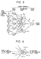
- Fig. 5 shows a neural network which is an equivalent circuit to an embodiment of a waveform equalizer according to the present invention, and which is implemented by simulation using a computer in order to design such a waveform equalizer.
- This is a multi-layer neural network formed of successive layers of neuron units, with interconnections by linking elements which are connected between the neuron units of a layer and neuron units of the preceding and succeeding layers.
- the neuron units are designated in general as U n,i , where "n" and "i” respectively denote the position of the layer containing that neuron unit and the position of the neuron unit within that layer, i.e.
- each of these delay lines DL can be considered to be a data register, through which input data values (described hereinafter, and referred to as learning input values) are successively shifted.
- each of these units of the input layer represents a linear amplifier which serves as an input buffer amplifier in the actual hardware neural network.
- the output signals from the input layer are coupled to respective ones of a set of neuron units U 2,1 , U 2,2 , U 2, 3 which constitute an intermediate layer of the neural network, with the output signals from the input layer being coupled through the aforementioned linking elements which multiply the output signals by respective weighting coefficients, these weighting coefficients being designated in general as W.
- Each of the neuron units has a specific non-linear input/output characteristic.
- each weighting coefficient is designated as W n,i,j , which indicates that the weighting coefficient is applied to the output signal from the j th neuron unit of the (n-1) th layer that is supplied to the i th neuron unit of the n th layer.
- these weighting coefficients W are variable and are determined mutually independently, however in the neural network of the actual waveform equalizer (i.e. the hardware configuration) the values of the weighting coefficients W are fixed (by respective resistor values).
- the values of these weighting coefficients W which connect the input layer to the intermediate layer can be considered to represent respective strengths of coupling between neuron units of the intermediate layer and neuron units of the input layer.
- respectively output signals produced from the neuron units of the intermediate layer are transferred through linking elements having respective weighting coefficients W to be inputted to a neuron unit of the output layer of the neural network.
- the output layer of the neural network consists of only a single neuron unit, that is to say a single output value is produced from that final neuron unit of the neural network in response to a specific combination of input signal signal values supplied to the input layer of the neural network. That final neuron unit of is designated as U 3, 1 .
- each of the units of the input layer of this embodiment is a linear amplifier.
- each of the neuron units of the input layer and output layer has a predetermined non-linear input/output characteristic, whereby the level of output signal produced therefrom varies in a known non-linear manner in accordance with the sum of the weighted input signal values applied thereto, and whereby respective weighting coefficients are selected to be positive or negative.
- Fig. 6 is a conceptual diagram to illustrate the input connections and operation of a neuron unit U n,i .
- Such a neuron unit can be considered to consist of an input section 50 and an output section 51.
- the input section 50 sums the weighted input signal values supplied thereto, with each of these input signal values having been multiplied by a corresponding weighting coefficient which is designated as W n,i,jn .
- the resultant sum output signal that is produced from the input section 50 of the neuron unit is designated as X n,i , and is supplied to the output section 51 of the neuron unit.
- a sequence of input signal values and a corresponding sequence of desired output values from the neural network are derived beforehand as described hereinafter, and stored in memory.
- teaching values are successively read out from memory, with the input values being supplied to the chain of "delay lines" DL1 to DL4.
- a specific combination of output values will be inputted in parallel to the neural network (i.e.
- a set of five values simulate a set of input values which are distributed at fixed intervas along the time axis.
- a corresponding teaching value is read out from memory, to Ce compared with the output value produced from the neural network (i.e. from the final neuron unit U 3,1 in this embodiment).
- the difference between that teaching value and the output value from the neural network is then applied in a learning algorithm, for modifying the respective values of the weighting coefficients W of the neural network, in a manner such as to reduce the amount of that difference.
- the learning operation is executed by using a back-propogation type of learning algorithm, whereby weighting coefficient updating processing proceeds from the output layer back to the input layer, i.e. in the reverse direction to the normal forward direction of processing.
- Such types of learning algorithm are now well known in the art, so that detailed description will be omitted.
- the units indicated as DL1 to DL4 would not be actual delay lines, but might be for example a set of four data registers.
- the contents of DL3 are shifted into DL4
- the contents of DL2 are shifted into DL3
- the contents of DL1 are shifted into DL32
- the most recent input signal value is set into DL1.
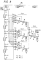
- Fig. 8 is a basic circuit diagram of this waveform equalizer embodiment. While all of the components shown in Fig. 5 are simulated by computer processing during the learning operation, i.e. implemented by software, the components of the circuit shown in Fig. 8 are generally-available hardware analog circuit elements, such as operational amplifiers, resistors etc.
- the circuit shown in Fig. 8 is equivalent to the neural network of Fig. 5, but with fixed values for the weighting coefficients W, with these fixed values being determined by by respective values of resistors R1 to R53. These fixed weighting coefficient values are determined beforehand bu a neural network learning operation using the computer-simulated neural network of Fig. 5, as described in detail hereinafter.
- an input signal i.e. a distorted digital signal which is produced from a recording and playback apparatus after having been recorded and reproduced, or is outputted from a digital signal transmission system after being received
- a chain of four series-connected delay lines 14, 15, 16, 17 which respectively corresponding to the four simulated "delay lines" DL1 to DL4 of the neural network circuit of Fig. 5
- That output signal and the respective output signals from the delay lines 14 to 17 are amplified by respective ones of a set of linear amplifiers 5, 6, 7, 8, and 9 which respectively correspond to the amplifiers U′ 1,1 to U′ 1,5 of the input layer of the equivalent neural network circuit of Fig 5.
- the output signals produced from the amplifiers 5 to 9 are coupled through the set of resistors R11, R21, R31, R41, R51, R12, R22, R32, R42, R52, R13, R23, R33, R43, and R53 to circuit units which function at the neuron units of the intermediate layer.
- These circuit units are signal conversion units each of which executes non-linear conversion of an input signal applied thereto.
- the conversion units of the intermediate layer respectively correspond to the neuron units U 2,1 to U 2,3 of the neural network of Fig. 5.
- each conversion unit of the intermediate layer is formed of a pair of operational amplifiers connected in series, with a diode pair connected at the output of the second operational amplifier, to provide a non-linear input/output characteristic.
- weighted input signals that are applied to such a neuron unit, some of the input signals are inputted to the inverting input terminal of the first operational amplifier of the series-connected pair (e.g. to the operational amplifier 1b, in the case of the neuron unit U 2,1 ), with the non-inverting input terminal of that operational amplifier being connected to ground potential, while other ones of these weighted input signals are applied to the inverting input terminal of the second one of the pair of series-connected operational amplifiers (e.g. to the operational amplifier 1a, in the case of the neuron unit U 2,1 ), with the non-inverting input terminal of that operational amplifier being connected to ground potential.
- each signal that is applied to the first operational amplifier e.g.
- each input signal that is supplied to the first operational amplifier of the pair can be considered to be multiplied by a fixed positive weighting coefficient (whose value is determined by the value of the resistor through which that signal is transferred), while each input signal that is supplied to the second operational amplifier of such a pair is in effect multiplied by a fixed negative weighting coefficient (whose absolute value is determined by the value of the resistor through which that signal is transferred).
- the output terminal of the second operational amplifier of each neuron unit is connected to ground potential through a pair of diodes which are connected in parallel with mutually opposing directions of polarity, i.e. the diode pairs 10, 11 and 12 connected to the outputs of the operational amplifiers 1a, 2a and 3a respectively of the actual neuron units in Fig. 8 which correspond to the neuron units U 2,1 , U 2,2 , U 2,3 of the neural network circuit of Fig. 5.
- the three neuron units of the intermediate layer in Fig. 8 are respectively formed of the series-connected pair of inverting-type operational amplifiers 1a, 1b, with the diode pair 10 connected at the output of operational amplifier 1a, the operational amplifiers 2b, 2a with the diode pair 11 connected at the output of operational amplifier 2a, and the operational amplifiers 3b, 3a with the diode pair 12 connected at the output of operational amplifier 3a
- the output signals produced from the neuron units of the intermediate layer in Fig. 8 are transferred through weighting resistors R1, R2, R3 respectively to the output neuron unit, corresponding to the output layer U 3,1 of the neural network circuit of Fig. 5.
- That output neuron unit is made up of series-connected inverting-type operational amplifiers 4b, 4a, with a diode pair 13 connected to the output of the second operational amplifier 4a. The output signal from the neural network is thereby developed across the diode pair 13.
- Each of the diode pairs 10 to 13 functions to provide a known form of non-linear input/output characteristic for the corresponding neuron unit. This will be described referring to Fig. 9, which shows the input/output characteristic of such a diode pair.
- a characteristic can be considered to consist of three different linear regions, which are designated as E1, E2 and E3 in Fig. 9.
- E1 and E3 the level of signal Voltage appearing across the diode pair is substantially constant (i.e. diode clipping occurs), while in the region E2 the output signal Y (i.e. the signal voltage appearing across the diode pair) varies substantially linearly with respect to input signal X.
- each of the neuron units of the actual waveform equalizer formed of a neural network shown in Fig. 8 can be configured from readily available circuit components, can have a simple circuit arrangement, can provide effectively negative or positive values for the weighting coefficients applied to the input signals applied thereto from neuron units of the preceding layer, and can have a known non-linear input/output characteristic that is formed of three linear regions.
- the central potential is assumed to be 0 V, i.e. the output signal Y produced from the output neuron unit varies between fixed positive and negative voltage levels.
- these positive and negative levels will be assumed to correspond to the digital 1 and 0 potentials respectively, while in addition the 0 V level of that output signal Y will be taken to represent a level of 0.5, i.e which is midway between the 1 and 0 digital potentials.
- the set of resistors (R11, R21, R31, R41, R51, R12, R22, R32, R42, R52, R13, R23, R33, R43, R53) which couple the output signals from the input layer of the neural network circuit in Fig. 8 to the neuron units of the intermediate layer, i.e. which transfer the output signals from the amplifiers 5, 6, 7, 8, 9 to the neuron units U 2,1 , U 2,2 , U 2,3 , will be collectively designated as the resistors R ji .
- the resistors (R1, R2, R3) which couple the output signals from the intermediate layer of the neural network circuit in Fig. 8 to the neuron units of the output layer, i.e. which transfer the output signals from the neuron units U 2,1 , U 2,2 , U 2,3 to the output neuron unit U 3,1 will be collectively designated as the resistors R j .
- the output neuron unit U 3,1 is formed of the pair of operational amplifiers 4a, 4b with the diode pair 13
- the weighting coefficients W 2,i,j in the neural network of Fig. 5 correspond to the resistors R ji
- the weighting coefficients W 3,i,j of the neural network of Fig. 5 correspond to the resistors R j .
- the respective values for the resistors R ji , R j are determined based upon the values obtained for the corresponding weighting coefficients.
- successive input signal values (which will be referred to in the following as learning signal values) are successively supplied to the neural network (i.e. to the "delay line" DL1 and the input layer unit U′ 1,1 ) at intervals which correspond to a fixed (real-time) period.
- each of these intervals will be assumed to correspond to one half of the bit period T of the digital playback signal from a CD, i.e. to one half of the minimum bit duration.
- the successive sets of learning input values that are outputted from the "delay lines" DL1 to DL4 are in effect distributed at successive T/2 intervals.
- each of the delay lines 14, 15, 16, 17 (respectively corresponding to the aforementioned "delay lines” DL1 to DL4 which apply input signals to the simulated neural network) provides a delay of T/2 in this embodiment.
- the input signal values supplied to the neuron units of the waveform equalizer neural network of Fig. 8 are the weighted output values from the preceding layer, i.e. in the case of the intermediate layer the input values are the output values from the input layer, after these have been respectively weighted by being transferred through the resistors R(j, i) (i.e. R11, R21, R31, R41, R51, R12, R22, R32, R42, R52, R13, R23, R33, R43, R53),which provide respectively independent fixed weighting coefficients.
- the resultant input values from the resistors are supplied to the neuron units of the intermediate layer, i.e. the units U 2,1 to U 2,3 .
- these weighted input signal values are applied to the inverting input terminals of the operational amplifiers 1a, 1b, 2a, 2b, 3a, 3b, to be additively combined.
- the input signal sum is subjected to non-linear conversion by the diode pair of that neuron unit (10, 11 or 12) and then outputted to the next layer, which is the output neuron unit.
- the circuit of Fig. 8 will in effect execute a similar type of judgement of the distorted playback signal that is supplied thereto as would an experienced human observer.
- the output signal produced from the waveform equalizer circuit of Fig. 8 will be closely similar to a signal that was originally recorded on a CD from which the playback signal is obtained, with level transitions of that output signal (corresponding to transitions between digital 1 and 0 levels) corresponding to those of the originally recorded signal. Accurate waveform equalization is thereby achieved.
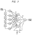
- Figs. 5 and 8 various other configurations for the neural network of the waveform equalizer could be utilized, other than that of Figs. 5 and 8. It may be found advantageous for example to apply respective weighted fixed DC bias inputs to each of the neuron units, as illustrated in Fig 7. The respective values for the weighting coefficients W applied to these bias inputs, supplied from a common DC bias source E B , are determined together with the other weighting coefficients W by a learning operation which is described hereinafter.
- circuit arrangement shown in Fig. 8 is intended only to show the basic elements of that circuit in a simple manner, for ease of understanding, and does not necessarily show all of the components (such as resistors for local negative feedback) which may be required in a practical circuit.
- the weighted input signals are inputted to the operational amplifiers as current signals, and all of the operational amplifers are of identical type, then it would be necessary to connect a resistor between the output of the first operational amplified of each neuron unit (e.g. 1b) and the input of the second amplifier of that unit (e.g. 1a), and to scale down the values of the input weighting resistors of each first operational amplifier accordingly.
- the procedure for determining suitable values for the resistors R ji , R j of the waveform equalizer of Fig. 8 is as follows.
- the procedure utilizes a suitably programed workstation (computer), and is based upon generating a simulated neural network of the form shown in Fig. 5, executing a learning operation to obtain suitable values for the weighting coefficients of that neural network, and then determining the respective values for the fixed weighting coefficients (i.e. resistor values) in the actual hardware neural network of the waveform equalizer.
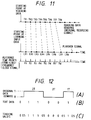
- FIG. 10 diagram (A) shows a portion of the waveform of an original signal which is used for learning.
- the learning operation utilizes data recorded on a CD in which the value of the aforemention minimum interval between transitions of the recorded data, Tmin, is made smaller than the standard value of 3 T.
- Tmin is made equal to T.
- each teaching value which occurs immediately before a transition of the original signal from the digital 0 to digital 1 state takes the value digital 0
- each teaching value which occurs immediately following a transition of the original signal from the digital 0 to digital 1 state takes the value digital 1
- each teaching value which coincides with a transition of the original signal between the digital 0 and digital 1 states takes a value which is midway between the digital 1 and 0 levels, which is indicated as a value of 0.5.
- the teaching values are tri-state values, rather than digital values in this example.
- the playback signal waveform from a CD corresponding to the original signal waveform portion showrn in diagram (A) will as shown in general be highly distorted.
- Periodic sampling of the playback signal is executed (as described hereinafter) to obtain successive values referred to in the following as learning input values, which respectively correspond to the aforementioned teaching values.
- Five of these learning input values are designated in diagram (C) as LV1 to LV5, which respectively correspond to the teaching values TV1 to TV5.
- the term “respectively corresponding” signifies “occurring at respectively identical positions along the data sequence”
- These positions, within the playback signal can be established (starting from a specific initial position, identified by a reference marker portion within the playback data) by using an appropriate clock signal as described hereinafter
- the learning input value designated as LV3 should ideally be 0 V, to correspond to the transition value 0.5 of the corresponding teaching value TV3.
- the learning input value LV4 should ideally be a positive voltage value corresponding to a predetermined digital 1 level.
- the learning input values will actually differ substantially from these ideal values.
- the learning operation is as follows.
- the learning input values are successively inputted to the "delay lines" DL1 to DL4 of the simulated neural network, such that during each learning interval (corresponding to T/2) there will be a set of five learning input values being supplied to the input layer of the neural network. While the learning input value LV3 is being supplied from DL2 (i.e.
- the resultant output value produced from the neural network as a result of the new combination of five input learning input values is compared with the teaching value TV4, corresponding to LV4, and the weighting coefficients are again updated accordingly based on the result of that comparison.
- the blocks designated as DL1 to DL4 in Fig. 5 do not represent actual delay elements, can be considered as respective data registers, through which the learning values are sequentially shifted, to obtain successive sets of five learning values that are inputted to the simulated neural network during respective learning intervals.
- the first learning input value is inputted to the unit U′ 1,1 of the first layer of the neural network, and a resultant output signal value obtained from the output unit U 3,1 of the neural network (although there is no teaching value actually corresponding to that output value).
- the second learning input value is then inputted to the unit U′ 1,1 while the first learning input value is being inputted to the second unit U′ 1,2 of the first layer, and a resultant output value obtained from the neural network. Again, there is no corresponding teaching value to that output value.
- the third learning input value is inputted to the unit U′ 1,1 while the second learning input value is being inputted to the second unit U′ 1,2 and the first learning input value is being inputted to the third unit U′ 1,2 of the input layer.
- a resultant output value is obtained from the neural network.
- there is a teaching value which is to be compared with that output value from the neural network i.e. the teaching value that corresponds to the first learning input value
- the learning algorithm will be executed for the first time.
- a sequence of teaching values TV1, TV2,.... are shown as occurring in a data sequence that is to be recorded on a recording medium, for example a CD.
- a playback signal is subsequently obtained from that CD, then due to such factors as disk rotation drive system inaccuracy during recording and playback, the values LV1, LV2 etc which respectively correspond to the teaching values TV1 etc. will not occur at regular intervals as measured with respect to a standard timebase.
- the above problem is overcome by using a PLL (phase locked loop) circuit to derive the clock signal component of the playback signal, and to use the derived clock signal to determine the sampling time points (i.e. the points R1, R2,.... in the example of Fig. 5).
- the time-axis deviations of the learning input values LV1, LV2, etc. will be identical to those of the sampling time points, so that the correct learning input values (i.e. respectively corresponding to the predetermined teaching values TV1, TV2, etc) can be accurately extracted from the playback signal by sampling that signal.
- the operation will be unaffected by deviations in the rotational speed of the CD 22.
- Fig 13 shows the apparatus required to record on a recording medium (in this case, a CD) data to be used in the neural network learning operation, which data will be referred to in the following as the learning data.
- the learning data are generated as a portion of original data that are produced from an original data source 20 and are supplied to a recording apparatus (i.e. cutting apparatus) 21 to be recorded on a CD 22.
- this original data includes an identifying marker portion, preceding the learning data, for use in precisely identifying the start of the learning data, and a preamble portion preceding the identifying marker portion, for initial stabilization of PLL operation.
- the original data are also supplied, as text data, to be recorded on a floppy disk 25 by a disk drive unit 24. If for example a portion of the original data is of the form shown in diagram (A) of Fig. 12, i.e. a sequence of 2 T periods at the digital 1 state, 2 T at the 0 state, followed by 1 T at the digital 1 state, then that portion could be represented as text data as a sequence of numeric symbols ....0, 1, 1, 0, 0, 1, 0, ......
- a playback apparatus 26 rotates the CD 22 to derive a playback signal from an optical pickup, with that playback signal being supplied to an A/D converter 28 and to a PLL 27.
- the A/D converter 28 periodically converts the playback signal to successive digital sample values at a sampling rate that is substantially higher than the data rate of the recorded data, i.e. with a sampling period that is much shorter than the aforementioned period T. It will be assumed that this sampling rate is 100 MHz.
- These digital samples are supplied to a sampling circuit 29.
- the PLL 27 extracts the data clock signal (having the 1 T period) from the playback signal, and also frequency-multiplies that extracted clock signal by 2 to obtain a sampling clock signal having the desired period of T/2 (described above referring to Fig. 10). That sampling signal is supplied to the sampling circuit 29, for selecting successive digital samples, e.g. to select the first digital sample which occurs at or immediately after each sampling time point defined by the sampling clock signal applied to the circuit 29. These selected sample values are stored in a sample data memory 30.
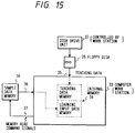
- the apparatus shown in Fig. 15 is used to set the learning input values and teaching values into a computer 33 (used as a work station) which executes the neural network simulation and learning operations.
- the learning data ire read out as text data from the floppy disk 25 by a disk drive unit 32 which is controlled by the computer 33, are transferred into the computer 33 through an input port 35, and are then converted to suitable form for use as teaching values in the neural network learning operation.
- the learning values are of the form described in Fig. 10 hereinabove (i.e. tri-state values of either digital 1 or 0 or the intermediate level 0.5)
- the text data sequence is converted by the computer 33 into a corresponding teaching value sequence, for example the sequence shown in diagram (C) of Fig. 12 in the case of the text data sequence of diagram (B) of Fig. 12.
- the teaching values thus obtained are successively stored in a teaching data region of an internal memory 34 of the computer 33.
- the sample data values are successively read out from the sample data memory 30 under the control of read command signals supplied from the computer 33, to be transferred through an input port 36 to the computer 33.
- the computer 33 judges each of these input sample values, to determine when these correspond to learning input values, and stores the learning input values in a learning input data region of the internal memory 34.
- the computer 33 examines the flow of input sample values from the memory 30 to detect the start of the learning data, as indicated by the aforementioned marker portion of the playback data from the CD.
- the computer 33 can then for example simply transfer each sample value which occurs, following that marker portion, into the learning input data memory as a learning input value (assuming that all of the sample values in the learning data portion are to be used as learning input values).
- the computer 33 can operate on successive groups (e.g. successive pairs) of these sample values which occur after the start of the learning data, to derive respective learning input values.
- the neural network learning operation described hereinabove is started, and continued until all of the learning data have been utilized, and a sufficient degree of convergence has been reached for the successively obtained values of neural network weighting coefficients derived in the learning operation.
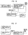
- Figs 16 and 17 The basic operations executed during the neural network learning operation and during normal functioning of the waveform equalizer (after fixed weighting coefficients have been established by the learning operation) are illustrated in Figs 16 and 17 respectively.
- the learning input values and teaching values that have been stored in the internal memory of the computer as described hereinabove are successively read out, with the learning input values being inputted to the neural network of Fig. 5, with the resultant output values produced from the simulated neural network being compared with respective teaching values, and the comparison results used in the learning algorithm, to establish updated values for the weighting coefficients of the neural network.
- a plurality of respectively differently distorted types of learning data are used in the learning operation.
- These different types of learning data will be referred to in the following as respective learning data categories, and can be generated for example by operating the playback apparatus 26 under respectively different conditions of incorrect adjustment of the optical pickup which reads data from the CD 22.
- respective learning data categories can be obtained in which distortion of the digital playback signal from the CD is the result of defocussing, spherical aberration, coma aberration along the direction of disk rotation, coma aberration that is opposite to the direction of disk rotation, etc.
- learning is firs: executed for one of these learning data categories, to obtain a final set of weighting coefficients for the neural network, then the learning is repeated using the next category of learning data, and so on for each of the categories.
- the overall flow of such learning operation is illustrated by the flow diagram of Fig. 22.
- the teaching data from the floppy disk 25 are transferred into the computer 33 as text data, and are then converted into a corresponding sequence of teaching values, e.g. tri-level teaching values as illustrated in diagram (C) of Fig. 12, with each transition between the digital 1 and 0 levels in the original signal being converted to an intermediate (0.5) level, and with the teaching values corresponding to sample values occurring at T/2 intervals.
- teaching data from the floppy disk 25 are transferred into the computer 33 as text data, and are then converted into a corresponding sequence of teaching values, e.g. tri-level teaching values as illustrated in diagram (C) of Fig. 12, with each transition between the digital 1 and 0 levels in the original signal being converted to an intermediate (0.5) level, and with the teaching values corresponding to sample values occurring at T/2 intervals.
- the set of teaching values TV1 to TV5 would be obtained as the sequence of values 0, 0, 0.5, 1, 1 (where "1" and "0" here represent digital 1 and 0 levels).
- the teaching values thus obtained are stored in the teaching data memory region of the internal memory 34.
- the playback signal for the first learning data category is then obtained from the CD 22, and the selected digital sample values are stored in the sample data memory 30 (step S3).
- step S4 initial values for the weighting coefficients of the simulated neural network are established, e.g. as random values.
- the first of the sample values that were stored in the sample data memory 30 is then read into the computer 33 and a simulated output is calculated (step S5), and a decision is made as to whether or not the timing of the output corresponds to that of the teaching values. If so, it is stored in the learning input value data memory region of the computer, then if the end of the playback data has not yet been reached (judged in step S8) the next sample value is read out from the sample data memory 30 and the above process repeated.
- the neural network learning operation is commenced (step S10), with successive ones of the stored learning input values being read out and supplied to the simulated neural network of Fig. 5.
- step S13 a decision is made as to whether or not all of the learning data categories have been processed. If not, a playback signal for obtaining the next learning data category is generated (step S14) and the operation then returns to step S3, in which that playback signal is sampled.
- the initial values to which the weighting coefficients are set in step S4 can be the values obtained for the preceding learning data category, which were stored in step S12.
- the above process is successively repeated for each of the learning data categories, to obtain a final set of weighting coefficients.
- each learning input value by interpolation of two successive sample values, as illustrated in Fig. 19.
- a learning input value LV m is obtained by interpolation between two adjacent sample values SV n and SV n+1 .
- each of the sample values obtained in the learning data portion of the playback signal is used as a learning input value
- the playback signal could be sampled at T/8 intervals, with the learning interval being T/2, and with each learning input value being calculated based on a combination of four successive sample values.
- CD playback apparatus which utilize an optical pickup which provides four playback signal channels, i.e. respectively derived from a set of four spatially separated pickup elements. These four playback signals can provide information to be used in systems which control the optical system of the pickup, for example the focussing.
- These four playback channel signals are preferably used to extract a more accurate data clock signal by the bit PLL of the above embodiment, as illustrated in Fig. 21.
- the playback signals of the four channels, designated as C1 to C4 are combined in a signal combining circuit 61, to obtain an input signal for the bit PLL 27. Higher stability and accuracy of PLL operation is thereby achieved.
- these four channel signals can be separately sampled, using the output signal from the PLL, to obtain 4-channel digital sample values which are stored in the sample data memory 30, to be subsequently transferred to the computer 33 for the learning operation.
- the four sample values are combined by the computer to obtain a single sample value, which is then operated on by the computer as described hereinabove for the case of single-channel operation.
- the computer 33 it is essential, for accurate learning operation of the embodiment described above, for the computer 33 to precisely identify the start of the learning data portion of the playback data which are inputted thereto. This is done by inserting an initial marker portion in the playback signal, containing a data pattern which will not otherwise occur in the playback data. Specifically, that marker portion consists of successive sets of 15 T periods of data at the digital 1 level and 15 T of data at the digital 0 level, as illustrated in Fig 20 which shows the data format of the playback signal used for learning operation. Firstly there is a preamble portion, i.e. a burst of data which is suitable for stabilizing the bit PLL operation.
- teaching values which are intermediate between the digital 0 and 1 levels i.e. 05 are utilized, and it has been found that this feature greatly increases the speed with which the learning operation can be executed to obtain final values for the weighting coefficients, and the accuracy of the waveform equalization that is provided by the finally designed waveform equalizer. It would be also possible to use a shorter value of learning interval than the value of T/2 used in the above embodiment. In that case, a plurality of intermediate values (between the digital 0 and 1 levels) could be used for the possible levels of the teaching values, in addition to the digital 0 and 1 levels.
- a second method of establishing the teaching values and learning input values to be used in the neural network learning operation will now be described.
- This method differs from that described above in that the bit PLL is not used to extract a clock signal from the playback signal. That is to say, referring to Fig. 14, the PLL 27 and sampling circuit 29 are omitted in this case.
- the system used can be as illustrated in Figs 13, 14 and 15.
- the playback signal from the CD 22 is converted to digital sample values at the very high sampling rate of the A/D converter 28 (e.g. 100 MHz), and these sample values are stored in the memory 30.
- a portion of the resultant data stored in the sample data memory 30 can for example be considered to be as illustrated in diagram. (A) of Fig. 23.
- the text data representing the corresponding portion of the teaching data could be as shown in diagram (B), or alternatively as shown in diagram (C) or diagram (D).
- these text data are transferred into the computer 33, they are converted into a sequence of digital 1 or 0 values, which occur at spacings corresponding to those of the learning input values, as illustrated in diagram (E) of Fig. 23..
- the corresponding portion of the teaching value data sequence is converted into 1,000 discrete digital values.
- These discrete digital teaching values are then transferred through a suitable digital low-pass filter, i.e. a FIR filter, to be converted into a sequence of discrete values which can take the 0 and 1 digital levels and also a plurality of levels which are intermediate between these digital levels, such that these teaching values conform to to an ideal teaching signal waveform as illustrated in diagram (F) in Fig. 23.
- the first part of the sample data held in the sample data memory 30 is transferred into the computer 33, to detect the aforementioned marker portion.
- successive sample values are transferred from the sample data memory 30 in response to read command signals sent from the computer 33, successive periodically occurring ones of these sample values are selected to be used as learning input values. This can be done for example by counting the number of times the read command signal is generated, to thereby determine the size of the learning interval, i.e. the separation between successive learning input values.
- the desired learning interval is 231 ns and a 100 MHz sampling frequency is used to obtain the sample values (so that the period of the sample values is 10 ns)
- the sample value then read out is selected by the computer 33 to become a learning input value and stored in the internal memory 34, while in addition that count number is increased to 24 each time 10 successive sample values have been selected.
- the average value of learning interval will be 231 ns, i.e. sample values will be periodically selected at spacings corresponding to 231 ns.
- This method of obtaining the learning input values has the basic disadvantage of requiring a very high accuracy of control of the speed of rotation of the CD 22, since only a fixed-frequency clock signal is used for sampling the playback signal to obtain the learning input values.
- a sammpling signal can be generated (e.g. by frequency-multiplying the extracted clock signal) that is phase-locked to the contents of the playback signal data, irrespective of changes in the speed of rotation of the CD from which the playback signal is obtained.
- each neuron unit i.e. signal conversion unit
- each neuron unit i.e. signal conversion unit
- the circuit of the waveform equalizer can have a very simple configuration.
- the learning computation processing based on the simulated neural network will also utilize such a form of non-linear input/output characteristic, the learning processing can be simple and efficient.
- a waveform equalizer formed of a neural network WE was constructed, using the design method described hereinabove in which a PLL is utilized in extracting sample values to be used as learning input values for the neural network learning operation.
- the circuit configuration was as shown in Fig. 8.
- Fig. 24(A) is a waveform photograph showing the effects of equalization by that waveform equalizer.
- Fig. 25(A) shows the analysis results obtained for the waveform equalizer, obtained by using a time interval analyzer.
- the test conditions were as follows:
- the recording medium used was a CD having a 2.8 times increase in recording density by comparison with the standard CD recording density (specifically, with the track pitch made 0.95 micron, to obtain a 1.68 times increase in recording density, and with the linear direction density increased by 1.67 times), and using optical recording with a linear velocity of 2.5 m/s for scanning the CD tracks by the pickup. That linear velocity is approximately twice the standard value of linear velocity used for a CD.
- Fig 24(A) shows eye pattern waveforms of an equalized digital sig obtained using the above embodiment of a waveform equalizer according to the present invention
- Fig. 25(A) shows the corresponding analysis results obtained, using a time interval analyzer
- Fig 24(B) similarly shows waveforms obtained for the case of waveform equalization using the prior art waveform equalizer of Fig. 1, and
- Fig. 25(B) shows the analysis results obtained for that prior art apparatus.
- Fig 24(C) shows the eye pattern waveforms for a playback signal with no waveform equalization applied
- Fig. 25(C) shows the corresponding analysis results obtained for the case of a playback signal with no waveform equalization applied.
- this waveform equalizer embodiment removes intersymbolic interference from the playback signal, and provides a distortion-free eye pattern.
- Figs. 25(A) to (C) showing the results of analysis of the waveform equalization by using a time interval analyzer (using a timebase of 1 ns and 105 samples), the data bits are spaced substantially equidistantly, as a result of the operation of the waveform equalizer WE, and clearly are well separated, with the amount of jitter standard deviation being small.
- the apparatus configuration is simple, and high-speed signal processing is made possible.
- the invention enables effective removal of distortion in a digital signal produced from a playback system or from a transmission system, by real-time operation, and with a level of performance being attained that has not been possible with prior art types of waveform equalizer.
Landscapes
- Engineering & Computer Science (AREA)
- Signal Processing (AREA)
- Artificial Intelligence (AREA)
- Evolutionary Computation (AREA)
- Physics & Mathematics (AREA)
- Biophysics (AREA)
- Theoretical Computer Science (AREA)
- Health & Medical Sciences (AREA)
- Life Sciences & Earth Sciences (AREA)
- Biomedical Technology (AREA)
- Computational Linguistics (AREA)
- General Engineering & Computer Science (AREA)
- Computer Networks & Wireless Communication (AREA)
- Data Mining & Analysis (AREA)
- General Health & Medical Sciences (AREA)
- Molecular Biology (AREA)
- Computing Systems (AREA)
- Neurology (AREA)
- General Physics & Mathematics (AREA)
- Mathematical Physics (AREA)
- Software Systems (AREA)
- Power Engineering (AREA)
- Cable Transmission Systems, Equalization Of Radio And Reduction Of Echo (AREA)
- Filters That Use Time-Delay Elements (AREA)
- Signal Processing For Digital Recording And Reproducing (AREA)
Applications Claiming Priority (2)
| Application Number | Priority Date | Filing Date | Title |
|---|---|---|---|
| JP31952/91 | 1991-01-31 | ||
| JP3031952A JP2797035B2 (ja) | 1991-01-31 | 1991-01-31 | ニューラルネットによる波形処理装置及びその設計方法 |
Publications (3)
| Publication Number | Publication Date |
|---|---|
| EP0498574A2 true EP0498574A2 (de) | 1992-08-12 |
| EP0498574A3 EP0498574A3 (en) | 1993-05-19 |
| EP0498574B1 EP0498574B1 (de) | 1997-07-23 |
Family
ID=12345299
Family Applications (1)
| Application Number | Title | Priority Date | Filing Date |
|---|---|---|---|
| EP92300838A Expired - Lifetime EP0498574B1 (de) | 1991-01-31 | 1992-01-31 | Einrichtung zur Wellenformentzerrung mit neuronalem Netzwerk und Verfahren zum Entwurf derselben |
Country Status (4)
| Country | Link |
|---|---|
| US (1) | US5361327A (de) |
| EP (1) | EP0498574B1 (de) |
| JP (1) | JP2797035B2 (de) |
| DE (1) | DE69220974T2 (de) |
Cited By (9)
| Publication number | Priority date | Publication date | Assignee | Title |
|---|---|---|---|---|
| EP0683489A3 (de) * | 1994-05-18 | 1996-04-03 | Matsushita Electric Industrial Co Ltd | Aufzeichnungs- und Wiedergabegerät mit Lernsignal. |
| EP0681291A3 (de) * | 1994-05-05 | 1996-05-01 | Thomson Brandt Gmbh | Verfahren zum Entzerren von verzerrten Datensignalen. |
| EP0752702A1 (de) * | 1995-07-07 | 1997-01-08 | Hewlett-Packard Company | Lesekanal mit künstlichem neuronalen Netzwerk |
| US5978782A (en) * | 1996-07-05 | 1999-11-02 | National Semiconductor Corporation | Neural network signal processor for magnetic storage channels |
| EP0674316A3 (de) * | 1994-03-19 | 2001-06-06 | Sony Corporation | Optische Platte und Verfahren und Gerät zur Aufzeichnung und Wiedergabe von dieser Platte |
| WO2018160465A1 (en) | 2017-03-01 | 2018-09-07 | Intel Corporation | Neural network-based systems for high speed data links |
| TWI695386B (zh) * | 2018-07-17 | 2020-06-01 | 旺宏電子股份有限公司 | 半導體電路及其操作方法 |
| CN112615676A (zh) * | 2020-12-18 | 2021-04-06 | 厦门亿芯源半导体科技有限公司 | 带有相位延迟补偿功能的高速光收发一体芯片驱动电路 |
| CN113095482A (zh) * | 2021-04-06 | 2021-07-09 | 西安邮电大学 | 基于bp神经网络的拉曼放大器增益值计算方法及系统 |
Families Citing this family (19)
| Publication number | Priority date | Publication date | Assignee | Title |
|---|---|---|---|---|
| US5504780A (en) * | 1994-01-06 | 1996-04-02 | Bell Communications Research Inc. | Adaptive equalizer using self-learning neural network |
| US5995924A (en) * | 1997-05-05 | 1999-11-30 | U.S. West, Inc. | Computer-based method and apparatus for classifying statement types based on intonation analysis |
| US7133331B2 (en) | 2000-12-28 | 2006-11-07 | Victor Company Of Japan, Limited | Recording medium having a substrate containing microscopic pattern of parallel groove and land sections and recording/reproducing equipment therefor |
| US7177262B2 (en) | 2002-04-19 | 2007-02-13 | Victor Company Of Japan, Ltd. | Reproducing system and corresponding information recording medium having wobbled land portions |
| JP2004013947A (ja) | 2002-06-04 | 2004-01-15 | Victor Co Of Japan Ltd | 情報記録担体、再生装置、記録装置、記録再生装置、再生方法、記録方法及び記録再生方法 |
| CN1310186C (zh) * | 2002-09-24 | 2007-04-11 | 中兴通讯股份有限公司 | 一种神经网络均衡器的优化训练方法 |
| US7869579B2 (en) * | 2005-12-09 | 2011-01-11 | Yahoo! Inc. | Selectable replay of buffered conversation in a VOIP session |
| US20070133523A1 (en) * | 2005-12-09 | 2007-06-14 | Yahoo! Inc. | Replay caching for selectively paused concurrent VOIP conversations |
| US7711582B2 (en) * | 2006-04-17 | 2010-05-04 | General Electric Company | Remote health application for the optimization of remote site visit frequency |
| US7593535B2 (en) * | 2006-08-01 | 2009-09-22 | Dts, Inc. | Neural network filtering techniques for compensating linear and non-linear distortion of an audio transducer |
| US10963775B2 (en) * | 2016-09-23 | 2021-03-30 | Samsung Electronics Co., Ltd. | Neural network device and method of operating neural network device |
| JP7212543B2 (ja) * | 2019-02-18 | 2023-01-25 | 日本放送協会 | 復号装置、ホログラム再生装置、及び復号方法 |
| CN109872730B (zh) * | 2019-03-14 | 2021-01-12 | 广州飞傲电子科技有限公司 | 音频数据的失真补偿方法、模型建立方法和音频输出设备 |
| US20210406661A1 (en) | 2020-06-25 | 2021-12-30 | PolyN Technology Limited | Analog Hardware Realization of Neural Networks |
| US12347421B2 (en) | 2020-06-25 | 2025-07-01 | PolyN Technology Limited | Sound signal processing using a neuromorphic analog signal processor |
| US11811425B2 (en) * | 2021-05-18 | 2023-11-07 | Western Digital Technologies, Inc. | Neural network soft information detector in a read channel |
| CN114996332B (zh) * | 2022-06-14 | 2025-03-25 | 北京经纬恒润科技股份有限公司 | 一种数据回放方法、装置及电子设备 |
| US11953987B1 (en) | 2022-09-16 | 2024-04-09 | Western Digital Technologies, Inc. | Trained states equalizer in a read channel |
| US12373130B2 (en) | 2023-02-02 | 2025-07-29 | Western Digital Technologies, Inc. | Global variance parameter based on mutual information in a data channel |
Family Cites Families (1)
| Publication number | Priority date | Publication date | Assignee | Title |
|---|---|---|---|---|
| JPH04216343A (ja) * | 1990-12-17 | 1992-08-06 | Sony Corp | 信号再生装置および方法 |
-
1991
- 1991-01-31 JP JP3031952A patent/JP2797035B2/ja not_active Expired - Lifetime
-
1992
- 1992-01-31 DE DE69220974T patent/DE69220974T2/de not_active Expired - Fee Related
- 1992-01-31 EP EP92300838A patent/EP0498574B1/de not_active Expired - Lifetime
- 1992-01-31 US US07/828,825 patent/US5361327A/en not_active Expired - Fee Related
Cited By (19)
| Publication number | Priority date | Publication date | Assignee | Title |
|---|---|---|---|---|
| USRE38638E1 (en) | 1994-03-19 | 2004-10-26 | Sony Corporation | Optical disk having a particular format to store user-selected data, such as video data or computer files, including a dedicated TOC region |
| USRE42962E1 (en) | 1994-03-19 | 2011-11-22 | Sony Corporation | Optical disk and method and apparatus for recording and then playing information back from that disk |
| EP1139338A3 (de) * | 1994-03-19 | 2006-10-11 | Sony Corporation | Optische Platte und Verfahren und Gerät zur Aufzeichnung und Wiedergabe von dieser Platte |
| EP0674316A3 (de) * | 1994-03-19 | 2001-06-06 | Sony Corporation | Optische Platte und Verfahren und Gerät zur Aufzeichnung und Wiedergabe von dieser Platte |
| USRE38502E1 (en) | 1994-03-19 | 2004-04-20 | Sony Corporation | Method and apparatus for recovering TOC and user information from an optical disk and using the TOC information to access user tracks |
| EP0681291A3 (de) * | 1994-05-05 | 1996-05-01 | Thomson Brandt Gmbh | Verfahren zum Entzerren von verzerrten Datensignalen. |
| US6134538A (en) * | 1994-05-05 | 2000-10-17 | Mager; Klaus | Procedure for equalizing distorted data signals |
| US5606538A (en) * | 1994-05-18 | 1997-02-25 | Matsushita Electric Industrial Co., Ltd. | Learning type signal recording and reproducing apparatus |
| EP0683489A3 (de) * | 1994-05-18 | 1996-04-03 | Matsushita Electric Industrial Co Ltd | Aufzeichnungs- und Wiedergabegerät mit Lernsignal. |
| US5699487A (en) * | 1995-07-07 | 1997-12-16 | Hewlett-Packard Company | Artificial neural network read channel |
| EP0752702A1 (de) * | 1995-07-07 | 1997-01-08 | Hewlett-Packard Company | Lesekanal mit künstlichem neuronalen Netzwerk |
| US5978782A (en) * | 1996-07-05 | 1999-11-02 | National Semiconductor Corporation | Neural network signal processor for magnetic storage channels |
| WO2018160465A1 (en) | 2017-03-01 | 2018-09-07 | Intel Corporation | Neural network-based systems for high speed data links |
| EP3590239A4 (de) * | 2017-03-01 | 2021-01-06 | INTEL Corporation | Auf neuronalem netzwerk basierte systeme für hochgeschwindigkeitsdatenverbindungen |
| TWI695386B (zh) * | 2018-07-17 | 2020-06-01 | 旺宏電子股份有限公司 | 半導體電路及其操作方法 |
| CN112615676A (zh) * | 2020-12-18 | 2021-04-06 | 厦门亿芯源半导体科技有限公司 | 带有相位延迟补偿功能的高速光收发一体芯片驱动电路 |
| CN112615676B (zh) * | 2020-12-18 | 2021-10-01 | 厦门亿芯源半导体科技有限公司 | 带有相位延迟补偿功能的高速光收发一体芯片驱动电路 |
| CN113095482A (zh) * | 2021-04-06 | 2021-07-09 | 西安邮电大学 | 基于bp神经网络的拉曼放大器增益值计算方法及系统 |
| CN113095482B (zh) * | 2021-04-06 | 2024-01-12 | 西安邮电大学 | 基于bp神经网络的拉曼放大器增益值计算方法及系统 |
Also Published As
| Publication number | Publication date |
|---|---|
| JP2797035B2 (ja) | 1998-09-17 |
| JPH04246906A (ja) | 1992-09-02 |
| US5361327A (en) | 1994-11-01 |
| EP0498574B1 (de) | 1997-07-23 |
| DE69220974T2 (de) | 1997-12-04 |
| EP0498574A3 (en) | 1993-05-19 |
| DE69220974D1 (de) | 1997-08-28 |
Similar Documents
| Publication | Publication Date | Title |
|---|---|---|
| US5361327A (en) | Waveform equalizer apparatus formed of neural network, and method of designing same | |
| US5287228A (en) | Peak detection method and apparatus therefor | |
| US7403460B2 (en) | Information recording and reproducing apparatus, evaluation method, and information recording and reproducing medium | |
| EP0109674B1 (de) | Mehrspur-PCM-Wiedergabegerät | |
| US5729517A (en) | Data detecting circuit | |
| JP3366389B2 (ja) | 伝送媒体からデジタル信号を入力する可変イコライザ手段を含む入力装置 | |
| JP2853650B2 (ja) | 信号処理装置 | |
| US6904086B2 (en) | Adaptive equalizer circuit | |
| JPH06295540A (ja) | ディジタル信号検出回路 | |
| CN100466508C (zh) | 锁相控制电路 | |
| JPH11273254A (ja) | ディスク記憶装置 | |
| US6532337B1 (en) | Digital-signal playback apparatus | |
| JP3331818B2 (ja) | ディジタル情報再生装置 | |
| US6381083B1 (en) | Multilevel signal equalization utilizing nonlinear maps | |
| US6188734B1 (en) | Data reproducing method and apparatus | |
| JP3515186B2 (ja) | 自動等化器 | |
| US5802505A (en) | Waveform signal equalizing method and apparatus and signal recording and reproducing apparatus | |
| JPS63304427A (ja) | 信号記録再生装置及び信号記録再生方法 | |
| KR100335616B1 (ko) | 데이타저장기기에 있어서신호검출방법및장치 | |
| JP2806331B2 (ja) | 波形等化回路 | |
| JP2978513B2 (ja) | 自動等化装置 | |
| JPH10198913A (ja) | 判定帰還等化方法及び判定帰還等化器 | |
| JP2861318B2 (ja) | データの検出方法 | |
| JPH05307623A (ja) | ニューラルネットによる波形処理装置の学習設計方法 | |
| JPH0714306A (ja) | 自動等化器の周辺回路 |
Legal Events
| Date | Code | Title | Description |
|---|---|---|---|
| PUAI | Public reference made under article 153(3) epc to a published international application that has entered the european phase |
Free format text: ORIGINAL CODE: 0009012 |
|
| AK | Designated contracting states |
Kind code of ref document: A2 Designated state(s): DE FR GB |
|
| PUAL | Search report despatched |
Free format text: ORIGINAL CODE: 0009013 |
|
| AK | Designated contracting states |
Kind code of ref document: A3 Designated state(s): DE FR GB |
|
| 17P | Request for examination filed |
Effective date: 19930923 |
|
| 17Q | First examination report despatched |
Effective date: 19951221 |
|
| GRAG | Despatch of communication of intention to grant |
Free format text: ORIGINAL CODE: EPIDOS AGRA |
|
| GRAH | Despatch of communication of intention to grant a patent |
Free format text: ORIGINAL CODE: EPIDOS IGRA |
|
| GRAH | Despatch of communication of intention to grant a patent |
Free format text: ORIGINAL CODE: EPIDOS IGRA |
|
| GRAA | (expected) grant |
Free format text: ORIGINAL CODE: 0009210 |
|
| AK | Designated contracting states |
Kind code of ref document: B1 Designated state(s): DE FR GB |
|
| REF | Corresponds to: |
Ref document number: 69220974 Country of ref document: DE Date of ref document: 19970828 |
|
| ET | Fr: translation filed | ||
| PLBE | No opposition filed within time limit |
Free format text: ORIGINAL CODE: 0009261 |
|
| 26N | No opposition filed | ||
| PGFP | Annual fee paid to national office [announced via postgrant information from national office to epo] |
Ref country code: DE Payment date: 20010122 Year of fee payment: 10 |
|
| PGFP | Annual fee paid to national office [announced via postgrant information from national office to epo] |
Ref country code: FR Payment date: 20010125 Year of fee payment: 10 |
|
| PGFP | Annual fee paid to national office [announced via postgrant information from national office to epo] |
Ref country code: GB Payment date: 20010131 Year of fee payment: 10 |
|
| REG | Reference to a national code |
Ref country code: GB Ref legal event code: IF02 |
|
| PG25 | Lapsed in a contracting state [announced via postgrant information from national office to epo] |
Ref country code: GB Free format text: LAPSE BECAUSE OF NON-PAYMENT OF DUE FEES Effective date: 20020131 |
|
| PG25 | Lapsed in a contracting state [announced via postgrant information from national office to epo] |
Ref country code: DE Free format text: LAPSE BECAUSE OF NON-PAYMENT OF DUE FEES Effective date: 20020801 |
|
| GBPC | Gb: european patent ceased through non-payment of renewal fee |
Effective date: 20020131 |
|
| PG25 | Lapsed in a contracting state [announced via postgrant information from national office to epo] |
Ref country code: FR Free format text: LAPSE BECAUSE OF NON-PAYMENT OF DUE FEES Effective date: 20020930 |
|
| REG | Reference to a national code |
Ref country code: FR Ref legal event code: ST |