EP0498736A2 - Diode laser DFB avec profile modifié du paramètre alpha - Google Patents
Diode laser DFB avec profile modifié du paramètre alpha Download PDFInfo
- Publication number
- EP0498736A2 EP0498736A2 EP92400328A EP92400328A EP0498736A2 EP 0498736 A2 EP0498736 A2 EP 0498736A2 EP 92400328 A EP92400328 A EP 92400328A EP 92400328 A EP92400328 A EP 92400328A EP 0498736 A2 EP0498736 A2 EP 0498736A2
- Authority
- EP
- European Patent Office
- Prior art keywords
- layer
- region
- laser diode
- active layer
- quantum well
- Prior art date
- Legal status (The legal status is an assumption and is not a legal conclusion. Google has not performed a legal analysis and makes no representation as to the accuracy of the status listed.)
- Withdrawn
Links
Images




Classifications
-
- H—ELECTRICITY
- H01—ELECTRIC ELEMENTS
- H01S—DEVICES USING THE PROCESS OF LIGHT AMPLIFICATION BY STIMULATED EMISSION OF RADIATION [LASER] TO AMPLIFY OR GENERATE LIGHT; DEVICES USING STIMULATED EMISSION OF ELECTROMAGNETIC RADIATION IN WAVE RANGES OTHER THAN OPTICAL
- H01S5/00—Semiconductor lasers
- H01S5/10—Construction or shape of the optical resonator, e.g. extended or external cavity, coupled cavities, bent-guide, varying width, thickness or composition of the active region
- H01S5/12—Construction or shape of the optical resonator, e.g. extended or external cavity, coupled cavities, bent-guide, varying width, thickness or composition of the active region the resonator having a periodic structure, e.g. in distributed feedback [DFB] lasers
-
- H—ELECTRICITY
- H10—SEMICONDUCTOR DEVICES; ELECTRIC SOLID-STATE DEVICES NOT OTHERWISE PROVIDED FOR
- H10H—INORGANIC LIGHT-EMITTING SEMICONDUCTOR DEVICES HAVING POTENTIAL BARRIERS
- H10H20/00—Individual inorganic light-emitting semiconductor devices having potential barriers, e.g. light-emitting diodes [LED]
- H10H20/80—Constructional details
- H10H20/81—Bodies
- H10H20/811—Bodies having quantum effect structures or superlattices, e.g. tunnel junctions
- H10H20/812—Bodies having quantum effect structures or superlattices, e.g. tunnel junctions within the light-emitting regions, e.g. having quantum confinement structures
-
- B—PERFORMING OPERATIONS; TRANSPORTING
- B82—NANOTECHNOLOGY
- B82Y—SPECIFIC USES OR APPLICATIONS OF NANOSTRUCTURES; MEASUREMENT OR ANALYSIS OF NANOSTRUCTURES; MANUFACTURE OR TREATMENT OF NANOSTRUCTURES
- B82Y20/00—Nanooptics, e.g. quantum optics or photonic crystals
-
- H—ELECTRICITY
- H01—ELECTRIC ELEMENTS
- H01S—DEVICES USING THE PROCESS OF LIGHT AMPLIFICATION BY STIMULATED EMISSION OF RADIATION [LASER] TO AMPLIFY OR GENERATE LIGHT; DEVICES USING STIMULATED EMISSION OF ELECTROMAGNETIC RADIATION IN WAVE RANGES OTHER THAN OPTICAL
- H01S5/00—Semiconductor lasers
- H01S5/06—Arrangements for controlling the laser output parameters, e.g. by operating on the active medium
- H01S5/062—Arrangements for controlling the laser output parameters, e.g. by operating on the active medium by varying the potential of the electrodes
- H01S5/06209—Arrangements for controlling the laser output parameters, e.g. by operating on the active medium by varying the potential of the electrodes in single-section lasers
- H01S5/0622—Controlling the frequency of the radiation
-
- H—ELECTRICITY
- H10—SEMICONDUCTOR DEVICES; ELECTRIC SOLID-STATE DEVICES NOT OTHERWISE PROVIDED FOR
- H10H—INORGANIC LIGHT-EMITTING SEMICONDUCTOR DEVICES HAVING POTENTIAL BARRIERS
- H10H20/00—Individual inorganic light-emitting semiconductor devices having potential barriers, e.g. light-emitting diodes [LED]
- H10H20/01—Manufacture or treatment
- H10H20/011—Manufacture or treatment of bodies, e.g. forming semiconductor layers
- H10H20/013—Manufacture or treatment of bodies, e.g. forming semiconductor layers having light-emitting regions comprising only Group III-V materials
-
- H—ELECTRICITY
- H01—ELECTRIC ELEMENTS
- H01S—DEVICES USING THE PROCESS OF LIGHT AMPLIFICATION BY STIMULATED EMISSION OF RADIATION [LASER] TO AMPLIFY OR GENERATE LIGHT; DEVICES USING STIMULATED EMISSION OF ELECTROMAGNETIC RADIATION IN WAVE RANGES OTHER THAN OPTICAL
- H01S5/00—Semiconductor lasers
- H01S5/06—Arrangements for controlling the laser output parameters, e.g. by operating on the active medium
- H01S5/0618—Details on the linewidth enhancement parameter alpha
-
- H—ELECTRICITY
- H01—ELECTRIC ELEMENTS
- H01S—DEVICES USING THE PROCESS OF LIGHT AMPLIFICATION BY STIMULATED EMISSION OF RADIATION [LASER] TO AMPLIFY OR GENERATE LIGHT; DEVICES USING STIMULATED EMISSION OF ELECTROMAGNETIC RADIATION IN WAVE RANGES OTHER THAN OPTICAL
- H01S5/00—Semiconductor lasers
- H01S5/06—Arrangements for controlling the laser output parameters, e.g. by operating on the active medium
- H01S5/062—Arrangements for controlling the laser output parameters, e.g. by operating on the active medium by varying the potential of the electrodes
- H01S5/06209—Arrangements for controlling the laser output parameters, e.g. by operating on the active medium by varying the potential of the electrodes in single-section lasers
-
- H—ELECTRICITY
- H01—ELECTRIC ELEMENTS
- H01S—DEVICES USING THE PROCESS OF LIGHT AMPLIFICATION BY STIMULATED EMISSION OF RADIATION [LASER] TO AMPLIFY OR GENERATE LIGHT; DEVICES USING STIMULATED EMISSION OF ELECTROMAGNETIC RADIATION IN WAVE RANGES OTHER THAN OPTICAL
- H01S5/00—Semiconductor lasers
- H01S5/06—Arrangements for controlling the laser output parameters, e.g. by operating on the active medium
- H01S5/062—Arrangements for controlling the laser output parameters, e.g. by operating on the active medium by varying the potential of the electrodes
- H01S5/0625—Arrangements for controlling the laser output parameters, e.g. by operating on the active medium by varying the potential of the electrodes in multi-section lasers
- H01S5/06255—Controlling the frequency of the radiation
- H01S5/06258—Controlling the frequency of the radiation with DFB-structure
-
- H—ELECTRICITY
- H01—ELECTRIC ELEMENTS
- H01S—DEVICES USING THE PROCESS OF LIGHT AMPLIFICATION BY STIMULATED EMISSION OF RADIATION [LASER] TO AMPLIFY OR GENERATE LIGHT; DEVICES USING STIMULATED EMISSION OF ELECTROMAGNETIC RADIATION IN WAVE RANGES OTHER THAN OPTICAL
- H01S5/00—Semiconductor lasers
- H01S5/10—Construction or shape of the optical resonator, e.g. extended or external cavity, coupled cavities, bent-guide, varying width, thickness or composition of the active region
-
- H—ELECTRICITY
- H01—ELECTRIC ELEMENTS
- H01S—DEVICES USING THE PROCESS OF LIGHT AMPLIFICATION BY STIMULATED EMISSION OF RADIATION [LASER] TO AMPLIFY OR GENERATE LIGHT; DEVICES USING STIMULATED EMISSION OF ELECTROMAGNETIC RADIATION IN WAVE RANGES OTHER THAN OPTICAL
- H01S5/00—Semiconductor lasers
- H01S5/10—Construction or shape of the optical resonator, e.g. extended or external cavity, coupled cavities, bent-guide, varying width, thickness or composition of the active region
- H01S5/1053—Comprising an active region having a varying composition or cross-section in a specific direction
- H01S5/1057—Comprising an active region having a varying composition or cross-section in a specific direction varying composition along the optical axis
-
- H—ELECTRICITY
- H01—ELECTRIC ELEMENTS
- H01S—DEVICES USING THE PROCESS OF LIGHT AMPLIFICATION BY STIMULATED EMISSION OF RADIATION [LASER] TO AMPLIFY OR GENERATE LIGHT; DEVICES USING STIMULATED EMISSION OF ELECTROMAGNETIC RADIATION IN WAVE RANGES OTHER THAN OPTICAL
- H01S5/00—Semiconductor lasers
- H01S5/10—Construction or shape of the optical resonator, e.g. extended or external cavity, coupled cavities, bent-guide, varying width, thickness or composition of the active region
- H01S5/1053—Comprising an active region having a varying composition or cross-section in a specific direction
- H01S5/106—Comprising an active region having a varying composition or cross-section in a specific direction varying thickness along the optical axis
-
- H—ELECTRICITY
- H01—ELECTRIC ELEMENTS
- H01S—DEVICES USING THE PROCESS OF LIGHT AMPLIFICATION BY STIMULATED EMISSION OF RADIATION [LASER] TO AMPLIFY OR GENERATE LIGHT; DEVICES USING STIMULATED EMISSION OF ELECTROMAGNETIC RADIATION IN WAVE RANGES OTHER THAN OPTICAL
- H01S5/00—Semiconductor lasers
- H01S5/10—Construction or shape of the optical resonator, e.g. extended or external cavity, coupled cavities, bent-guide, varying width, thickness or composition of the active region
- H01S5/12—Construction or shape of the optical resonator, e.g. extended or external cavity, coupled cavities, bent-guide, varying width, thickness or composition of the active region the resonator having a periodic structure, e.g. in distributed feedback [DFB] lasers
- H01S5/124—Construction or shape of the optical resonator, e.g. extended or external cavity, coupled cavities, bent-guide, varying width, thickness or composition of the active region the resonator having a periodic structure, e.g. in distributed feedback [DFB] lasers incorporating phase shifts
-
- H—ELECTRICITY
- H01—ELECTRIC ELEMENTS
- H01S—DEVICES USING THE PROCESS OF LIGHT AMPLIFICATION BY STIMULATED EMISSION OF RADIATION [LASER] TO AMPLIFY OR GENERATE LIGHT; DEVICES USING STIMULATED EMISSION OF ELECTROMAGNETIC RADIATION IN WAVE RANGES OTHER THAN OPTICAL
- H01S5/00—Semiconductor lasers
- H01S5/20—Structure or shape of the semiconductor body to guide the optical wave ; Confining structures perpendicular to the optical axis, e.g. index or gain guiding, stripe geometry, broad area lasers, gain tailoring, transverse or lateral reflectors, special cladding structures, MQW barrier reflection layers
- H01S5/2054—Methods of obtaining the confinement
- H01S5/2077—Methods of obtaining the confinement using lateral bandgap control during growth, e.g. selective growth, mask induced
-
- H—ELECTRICITY
- H01—ELECTRIC ELEMENTS
- H01S—DEVICES USING THE PROCESS OF LIGHT AMPLIFICATION BY STIMULATED EMISSION OF RADIATION [LASER] TO AMPLIFY OR GENERATE LIGHT; DEVICES USING STIMULATED EMISSION OF ELECTROMAGNETIC RADIATION IN WAVE RANGES OTHER THAN OPTICAL
- H01S5/00—Semiconductor lasers
- H01S5/20—Structure or shape of the semiconductor body to guide the optical wave ; Confining structures perpendicular to the optical axis, e.g. index or gain guiding, stripe geometry, broad area lasers, gain tailoring, transverse or lateral reflectors, special cladding structures, MQW barrier reflection layers
- H01S5/22—Structure or shape of the semiconductor body to guide the optical wave ; Confining structures perpendicular to the optical axis, e.g. index or gain guiding, stripe geometry, broad area lasers, gain tailoring, transverse or lateral reflectors, special cladding structures, MQW barrier reflection layers having a ridge or stripe structure
- H01S5/227—Buried mesa structure ; Striped active layer
- H01S5/2272—Buried mesa structure ; Striped active layer grown by a mask induced selective growth
-
- H—ELECTRICITY
- H01—ELECTRIC ELEMENTS
- H01S—DEVICES USING THE PROCESS OF LIGHT AMPLIFICATION BY STIMULATED EMISSION OF RADIATION [LASER] TO AMPLIFY OR GENERATE LIGHT; DEVICES USING STIMULATED EMISSION OF ELECTROMAGNETIC RADIATION IN WAVE RANGES OTHER THAN OPTICAL
- H01S5/00—Semiconductor lasers
- H01S5/30—Structure or shape of the active region; Materials used for the active region
- H01S5/34—Structure or shape of the active region; Materials used for the active region comprising quantum well or superlattice structures, e.g. single quantum well [SQW] lasers, multiple quantum well [MQW] lasers or graded index separate confinement heterostructure [GRINSCH] lasers
- H01S5/3428—Structure or shape of the active region; Materials used for the active region comprising quantum well or superlattice structures, e.g. single quantum well [SQW] lasers, multiple quantum well [MQW] lasers or graded index separate confinement heterostructure [GRINSCH] lasers layer orientation perpendicular to the substrate
Definitions
- the present invention generally relates to semiconductor devices and more particularly to a DFB laser diode having a capability of shifting its oscillation frequency in a wide frequency range.
- laser diode is an essential device for producing the coherent optical beam.
- the laser diode is required to oscillate at a single frequency with a narrow spectrum.
- the laser diode has a capability of shifting its frequency in response to an electric information signal.
- the frequency-shift keying (FSK) modulation of optical beam is achieved.
- a tunable laser diode is useful in realizing a frequency multiplex telecommunication system.
- a tunable DFB laser diode As a laser diode for use in such optical telecommunication systems, a tunable DFB laser diode is proposed in the Japanese Patent Applications 1-184144, 1-235929, 1-235930 and 1-235928 that correspond to the United States Patent Application S.N.552,116 and the European patent application No.90307626.3, which are incorporated herein as reference.
- a non-uniform intensity profile of optical radiation is induced in the laser diode along a longitudinal axis thereof such that a maximum of radiation intensity occurs generally in correspondence to the longitudinal center of the laser diode.
- a modulation current selectively in correspondence to the maximum of the radiation that in turn corresponds to the maximum depletion of carriers, one can change the oscillation frequency of the laser diode in a wide range of frequency.
- the non-uniform radiation profile is artificially induced by providing a ⁇ /4-shift point generally at the longitudinal center of the corrugation grating that is provided for establishing the Bragg reflection in the DFB laser diode.
- Such a strong depletion of carriers caused at the longitudinal center of the laser diode in response to the strong optical radiation is called "axial hole burning effect.”
- FIG.1 shows the simplified structure of a conventional DFB laser diode having the ⁇ /4 phase shift point in the corrugation grating of the waveguide layer.
- the inventor of the present invention has found that the magnitude of frequency shift obtained as a result of the modulation of the injection current is not as large as expected from the change of the injection current.
- this problem will be examined in detail with reference to FIGS.1 - 4.
- the explanation will be given for the device of FIG.1 that has only one electrode in the longitudinal direction.
- the conventional DFB laser diode has a substrate 1 of an n-type compound semiconductor material such as InP, and a waveguide layer 2 of another n-type compound semiconductor material is provided on the substrate 1.
- a corrugation grating 1A is provided for causing the Bragg reflection.
- a ⁇ /4-phase shift point 1B is provided for causing the concentration of optical radiation at the longitudinal center of the laser diode.
- the continuous repetition of corrugation grating is discontinued such that the corrugation grating at the right of the point 1B is shifted in phase with respect to the corrugation grating at the left of the point 1B by the phase equal to ⁇ /4, where ⁇ represents the wavelength of the corrugation grating.
- an undoped active layer 3 is provided and a clad layer 4 of p-type compound semiconductor material is provided on the active layer 3. Further, an electrode 5 is provided on the clad layer 4 and another electrode 6 is provided on the lower major surface of the substrate 1.
- a drive current is injected via the electrodes 5 and 6 and there is caused a stimulated emission in the active layer 3.
- the optical beam thus produced is guided along the waveguide layer 2 while experiencing the periodically changing refractive index profile that is caused by the corrugation grating. Thereby, the optical radiation is reflected back and forth by the Bragg reflection.
- FIG.2 shows the intensity distribution of the optical radiation produced in the active layer 3 of the device of FIG.1 in the longitudinal direction. As shown therein by the continuous line, there appears a maximum in the optical intensity distribution in correspondence to the ⁇ /4-shift point 1B.
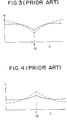
- the inventor of the present invention has discovered that the change of the drive current, intended to cause the shift in the carrier density profile and hence the refractive index profile for the frequency shift modulation, does not cause the desired parallel shift of the refraction index profile but a mere modification without substantial shift as shown by the broken lines in FIGS.3 and 4.
- the increased injection current certainly causes an increased carrier density at both longitudinal ends of the laser diode, while such an increase in the injection current simultaneously causes an enhancement of the depletion of the carriers at the central part corresponding to the ⁇ /4-shift point 1B. It is believed that such a depletion of the carrier is caused as a result of the increased intensity of optical radiation that facilitates the recombination.
- FIG.4 shows the increased intensity of the optical radiation by the broken line.
- the overall carrier density that is the carrier density averaged in the longitudinal direction does not shift as is expected from the increased injection current.
- Another and more specific object of the present invention is to provide a DFB laser diode capable of shifting the oscillation frequency in a wide frequency range.
- Another object of the present invention is to provide a DFB laser diode having a linewidth enhancement factor that is modified in a longitudinal direction of the laser diode, wherein the laser diode includes: a first region located generally in correspondence to the longitudinal center of the laser diode and characterized by a first linewidth enhancement factor; and a second region located at both sides of the first region in the longitudinal direction and characterized by a second linewidth enhancement factor; wherein there is a discontinuity formed between the first and second linewidth enhancement factors at the boundary between the first region and the second region.
- the present invention one can suppress the shift of the refractive index in the first region, and the canceling out of the overall refractive index shift in the first region and the second region is thereby minimized. Thereby, a change of the refraction index occurs in the entire length of the laser diode and the oscillation frequency of laser diode changes in a wide range of frequency.
- Another object of the present invention is to provide a process for fabricating a DFB laser diode that includes, in an active layer thereof, a first region having a first linewidth enhancement factor and a second region disposed at both sides of the first region in a longitudinal direction of the laser diode, said second region having a second linewidth enhancement factor that is different from the first linewidth enhancement factor, wherein the active layer has a multiple quantum well structure with a thickness of each semiconductor layer forming the multiple quantum structure being changed in the first and second regions, comprising the steps of depositing each layer of the quantum well structure using a pair of elongated masks generally extending parallel with each other in the longitudinal direction of the laser diode, said masks being disposed with a predetermined separation in correspondence to the active layer, wherein each mask has a lateral projection area projecting laterally in a direction away from the other mask.
- the wavelength of the optical radiation produced in the correspondence to the first region becomes longer than the wavelength that is produced in the second region where the thickness of the quantum well layer is smaller.
- the corrugation of the DFB laser diode is tuned to the optical radiation that is produced in the second region, such a deviation of the wavelength in the first region results in an increase in the differential gain, and such an increase in the differential gain causes a decrease of the linewidth enhancement factor.
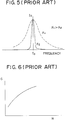
- FIG.5 shows the spectrum of the optical beam produced by a laser diode
- FIG.6 shows the relationship between the gain G of the laser diode and the carrier density N that is formed in the active layer of the laser diode.
- the coherent optical beam is produced as a result of the stimulated emission.
- the stimulated emission it is well known that the emission of photons occurs as a result of interaction between the carriers and the quantized electromagnetic field, and the photons are emitted to the mode that is already occupied by the photons.
- the optical beam that propagates back and forth in the active layer induces emission of photons therein with a phase synchronized with the phase of the optical beam. Thereby, the amplification of the coherent optical beam is achieved.
- the spontaneous emission In the laser diode, there exists another mechanism for producing the optical radiation known as the spontaneous emission.
- the carriers cause an interaction with a fluctuating quantum field of vacuum, and the emission of photons is made to the mode where there is no or few photons.
- the spontaneous emission the optical radiation produced by the laser diode inevitably shows a broad spectrum due to the random phase and wavelength of the optical radiation produced by this mechanism.
- linewidth enhancement factor ⁇ that is defined as ⁇ ⁇ (dn/dN)/(dG/dN) wherein the quantity G represents the gain of the laser diode and the term dG/dN represents the differential gain.
- the linewidth enhancement factor ⁇ represents the contribution of the spontaneous emission to the overall radiation formed in the active layer of the laser diode. In other words, the factor ⁇ represents the degree of broadening of the spectrum of the laser diode.
- the linewidth enhancement factor ⁇ is generally constant along its longitudinal axis except for a small, gradual decrease at the central part thereof.
- dn/dN is determined by the composition and structure of the active layer of the laser diode, while the term dG/dN does not change significantly in the laser diode.
- FIG.6 shows the gain G as a function of the carrier density N.
- the gain increases generally monotonously with the carrier density N, with the differential gain dG/dN decreasing gradually with the carrier density N.
- the slope dG/dN increases slightly in this part of the laser diode. This in turn results in the aforementioned slight decrease of the factor ⁇ .
- this effect is not significant, as the slope of the curve shown in FIG.6 does not change significantly even when the carrier density N is changed.
- the change of the refractive index in response to the carrier density is thereby represented approximately as dn ⁇ ⁇ dN. wherein it is assumed that the term dG/dN is constant. This relationship indicates that one can suppress the change of the refractive index of the active layer by reducing the value of the parameter ⁇ .
- the unwanted increase of the refractive index at the central part of the active layer of the laser diode as shown in FIG.4 is suppressed by modifying the value of the linewidth enhancement factor ⁇ in correspondence to the longitudinal center of the laser diode.
- FIG.7 shows the principle of the present invention.
- the factor ⁇ is changed stepwise in three distinct parts along the longitudinal direction, i.e. a first part or part I at a first end of the laser diode, a second part or part 11 at a longitudinal center and a third part or part 111 at a second, opposite end, such that the linewidth enhancement factor ⁇ is decreased in correspondence to the central part 11.
- the factor ⁇ may be the same.
- FIG.8 shows the longitudinal cross section of the DFB laser diode according to a first embodiment of the present invention.
- the laser diode is constructed on a substrate 11 of n-type InP, wherein the substrate 11 has a corrugated upper major surface 11a that establishes the Bragg reflection in the longitudinal direction as usual in the art. Further, there is provided a ⁇ /4-shift point 11A in the corrugation grating 11a generally in correspondence to the central part of the laser diode.
- the substrate 11 is doped with an impurity concentration level of 1 X 1018cm ⁇ 3.
- the waveguide layer 12 has a substantially flat upper major surface and has a thickness that changes between 100 nm and 150 nm in correspondence to the peak and valley of the corrugation grating 11A.
- an active layer 13 is provided on the waveguide layer 12 with a thickness of 150 nm for producing the optical radiation as a result of the stimulated emission.
- the active layer 13 is formed of three distinct regions 13A, 13B and 13C aligned in the longitudinal direction of the laser diode with longitudinal lengths L1, L2 and L3, wherein the region 13B is located at the longitudinal center. It should be noted that the regions 13A, 13B and 13C correspond respectively to the regions I, II and III of FIG.7, in which the region 13B is formed at the longitudinal center in correspondence to the ⁇ /4-shift point 11A.
- a clad layer 14 of p-type InP having an impurity concentration level of 5 X 1017cm ⁇ 3 and a thickness of 150 nm.
- a contact layer 15 of p-type InGaAsP is provided on the clad layer 14 with a thickness of 0.5 ⁇ m.
- a p-type electrode layer 16 having a layered structure of Ti/Pt/Au with a thickness of about 1 ⁇ m as usual.
- a silicon nitride anti-reflection film 18 is provided on both longitudinal ends of the laser diode with a thickness of 200 nm.
- the regions 13A and 13C of the layer 13 are formed of undoped InGaAsP, wherein the length L1 and the length L3 are set to about 300 ⁇ m.
- the length L2 of the region 13B is set to about 600 ⁇ m.
- the laser diode has a total longitudinal length L of about 1200 ⁇ m.
- the regions 13A and 13C are formed of a bulk crystal of InGaAsP while the region 13B has a multiple quantum well (MQW) structure.
- MQW multiple quantum well
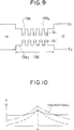
- FIG.9 shows the band diagram of the region 13B taken along the cross section shown in FIG.8 by a line 9-9′.
- the region 13B includes an alternate repetition of layers 13 B2 and 13 B2 , wherein the layer 13B1 is formed of undoped InGaAs layer having a thickness of 90 nm and acting as a quantum well layer, while the layer 13 B2 is formed of undoped InGaAsP layer having a thickness of 130 nm and acting as a barrier layer.
- the conduction band is shown by E c while the valence band is shown by E v .
- the layer 131 has a band gap that is substantially smaller as compared with the barrier layer 132 and there is obtained an effective confinement of carriers in the quantum well formed by the layer 131.
- the MQW structure thus formed of the layers 131 and 132 are sandwiched vertically by a pair of SCH (separate confinement heterostructure) layers 13B3 of InGaAsP each having a thickness of 265 nm.
- the layer unit formed of the layers 13B1 and 13B2 is repeated for about five times in the active layer 13.
- the MQW structure By forming the MQW structure as such, there are formed discrete quantum levels QL and QL′ in each quantum well as a result of the vertical confinement of the carriers. Thereby, the recombination of carriers occurs selectively and intensively between these quantum levels and the efficiency of stimulated emission is improved substantially. This in turn increases the term of the differential gain dG/dN in Eq.(1) in correspondence to the region 13B. In Eq.(1), the linewidth enhancement factor ⁇ decreases with the increase of the term dG/dN.
- the injection current is supplied across the electrodes 16 and 17, and the carriers thus injected are accumulated in the active layer 13 as usual.
- an efficient recombination of carriers occurs when the injection current exceeds a predetermined threshold.
- the intensity of optical beam is enhanced at the longitudinal central part of the laser diode, and this non-uniform profile of the optical intensity is enhanced by the ⁇ /4-shift point 11A, similarly to the device of FIG.1.
- the carrier profile similar to FIG.3 and characterized by the depletion of carriers at the longitudinal central part of the device is obtained.
- FIG.10 shows the refractive index profile that is achieved by the present invention, wherein the continuous line represents the initial state and the broken line represents the state realized in response to the increase of the injection current.
- the refraction index profile that is achieved by the conventional device of FIG.1 is shown in FIG.10 by a one-dotted chain.
- the carrier distribution profile substantially identical with that shown in FIG.3 is obtained also in the device of the present embodiment as a result of the axial hole burning.
- the unwanted increase of the refractive index in response to the increase of the injection current at the central part of the laser diode is suppressed in the device of the present embodiment as can be seen clearly in FIG.10. Thereby, there occurs an overall shift of the refractive index in the downward direction in FIG.10 and there occurs a corresponding large shift of the oscillation wavelength.
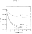
- FIG.11 shows the shift of the oscillation wavelength in response to the change of the injection current.
- the vertical axis represents the oscillation wavelength while the horizontal axis represents the injection current normalized with respect to the initial state.
- the broken line designated as "a” represents the wavelength shift for the device wherein the parameter ⁇ is set to about 3.5 throughout the device while the one-dotted line designated as "b" represents the wavelength shift for the device wherein the parameter ⁇ is set to about 5.0.
- the continuous line designated as "c” represents the wavelength shift for the device of the present embodiment wherein the parameter ⁇ is set to 3.5 at the region 13B. In the regions 13A and 13C, the parameter ⁇ is set to 5.0.
- the device of the present embodiment provides the largest shift of wavelength in response to the modulation of the injection current. Further, it should be noted that the device of the present embodiment provides a sharp spectrum in correspondence to the use of the reduced parameter ⁇ at the central region 13B of the laser diode. It will be noted that the device having the parameter ⁇ of 5.0 (curve b), the magnitude of shift of oscillation wavelength is comparable with the device of the present embodiment. In this device, however, it will be noted that the spectrum of the optical beam inevitably becomes diffuse because of the large value of the parameter ⁇ .
- the laser diode of FIG.8 may be fabricated by various processes. For example, one may deposit the InGaAsP layer in correspondence to the active layer 13 by the MBE process, and remove a part of the layer 13 in correspondence to the region 13B by an RIE process until the waveguide layer 12 is exposed. After covering the layer 13 by a silicon oxide mask in correspondence to regions 13A and 13C, the SCH layer 13B3 is deposited on the exposed part of the waveguide layer 12 by the MBE process. Further, the layers 13B1 and 13B2 are deposited alternately by the MBE process on the layer 13B3. After the layers 13B1 and 13B2 are repeated for a predetermined number of times, the SCH layer 13B3 is grown again and the formation of the layer 13 is completed.
- the clad layer 14 and the contact layer 15 are grown as usual and the electrodes 16 and 17 are provided. Further, the anti-reflection film 18 is formed on both longitudinal ends and the fabrication of the DFB laser diode is completed.
- the formation of the waveguide layer 12 and the corrugation grating 11a is well known for example from the prior art reference cited at the introductory part of the present specification, further description of the fabrication process will be omitted.
- FIG.12(A) shows a mask pattern 22 that is used for growing a semiconductor layer on a selected part of a substrate 21, while FIG.12(B) shows a profile of the thickness of the semiconductor layer grown on the substrate 21 by using the mask pattern 22.
- the mask pattern 22 includes two elongated parts, a first mask 22a and a second mask 22b extending generally parallel with each other with a separation W. More specifically, the masks 22a and 22b define therebetween a striplike region having a width set equal to W, and the deposition of the semiconductor layer occurs in correspondence to this strip-like region. Further, each of the masks 22a and 22b has a laterally projecting area 22a1 and 22b2 such that the areas 22a1 and 22b2 extend in the mutually opposing directions.
- the masks 22a and 22b are formed of silicon oxide.
- silicon oxide mask it is known that the thickness of the epitaxial layer that is grown on the substrate in correspondence to the part that is located between the projecting areas 22a1 and 22a2 increases as compared with the part located between the straight parts of the masks 22a and 22b. See for example J. Finders et al., J. Crystal Growth, 107, pp.151-155 (1991). Although the reason of this phenomenon is not fully understood at the moment, it is believed that the atoms of the group III or group V element deposited on the masks 22a and 22b migrate on the surface of the mask and deposited when reached the exposed surface of the substrate 21.
- the areas 22a1 and 22b1 collect larger number of atoms as compared with the rest of the part of the mask, and these atoms increase the thickness of the epitaxial layer at the part located between the parts 22a1 and 22b1 as shown in FIG.12(B).
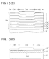
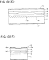
- FIGS.13(A) - 13(F) the fabrication process of the DFB laser diode of the present invention will be described with reference to FIGS.13(A) - 13(F).
- those parts that correspond to the parts described already with reference to previous embodiments will be designated by the same reference numerals and the description thereof will be omitted.
- a silicon oxide layer 31 is provided on the waveguide layer 12 with a thickness of about 0.1 ⁇ m and patterned subsequently to form a mask pattern 32 as shown in the plan view of FIG.13(B).
- the mask pattern 32 includes a pair of generally parallel masks 32a and 32b, wherein the mask 32a has a laterally projecting area 32a1 and the mask 32b has a laterally projecting area 32b1.
- the masks 32a and 32b are disposed symmetrically with each other, with the mask area 32a1 and the mask area 32b1 extending in the mutually opposite directions. Thereby, there is formed a strip-like region between the mask 32a and the mask 32b with a width W such that the upper major surface of the waveguide layer 12 is exposed at the strip-like region.
- the strip-like region is defined laterally by a pair of straight edges. In the illustrated example, the width W is set to 2 ⁇ m.
- each of the masks 32a and 32b has a width A that is set to about 4 ⁇ m in correspondence to where there is no lateral projecting areas 32a and 32b, while each mask parts 32a1 and 32b1 has a width B of about 10 ⁇ m in correspondence to the parts 32a1 and 322. It should be noted that the parts 32a1 and 32b1 correspond to the region 13B defined in FIG.8 while the rest of the part of the masks 32a and 32b corresponds to the regions 13A and 13C of the laser diode. See FIG.13(B).
- the deposition of an active layer 13′ corresponding to the active layer 13 of FIG.8 is made by the metal organic vapor phase epitaxy (MOVPE) process by alternately depositing a quantum well layer 13a′ of InGaAsP and a barrier layer 13b′ of InGaAs, wherein the barrier layer 13b′ is deposited first on the upper major surface of the waveguide layer 12. See FIG.13(C).
- the gases such as TMI, TMG, arsine and phosphine are introduced into a reaction vessel as the source of the layer 13a′, while the gases such as TMI, TMG and arsine are introduced as the source of the layer 13b′.
- the gases TMI, TMG, arsine and phosphine are introduced with respective flowrates of 0.5 SCCM, 0.5 SCCM, 0.5 SCCM and 0.5 SCCM.
- the growth of the layer 13b′ is made while introducing the gases TMI, TMG and arsine with respective flowrates of 0.5 SCCM, 0.5 SCCM and 0.5 SCCM.
- the layer 13′ has a thickness of about 57 nm in correspondence to the region 13B while the layer 13′ has the thickness of about 79 nm in correspondence to the regions 13A and 13C.
- the silicon oxide masks 33a and 33b are removed by etching such as a wet etching process in a hydrofluoric acid, and the clad layer 14 is deposited on the structure thus obtained by the MOVPE process. Further, the contact layer 15 is grown on the clad layer 14, and the electrodes 16 and 17 are provided respectively on the upper major surface of the contact layer 15 and the lower major surface of the substrate 11 as usual.
- the upper major surface of the contact layer 15 is exposed in correspondence to the strip-like region extending in the longitudinal direction of the laser diode between the parts 16a and 16b, and the electrode 16 establishes a contact with the contact layer 15 in correspondence to the exposed part of the layer 15.
- the electrode 16 establishes a contact with the contact layer 15 in correspondence to the exposed part of the layer 15.
- the increased thickness of the quantum well layers 13′a increases the wavelength of the optical radiation that is produced as a result of recombination of the carriers in the region 13B.
- the optical radiation produced in the region 13B of the laser diode has a wavelength that is deviated from the wavelength of the optical radiation that is produced in the regions 13A and 13C in the longer wavelength side.
- the corrugation grating 11a is tuned to cause the Bragg reflection for the optical radiation produced in the first and third regions 13A and 13C.
- the DFB laser diode of the present embodiment also shows the distribution of the linewidth enhancement factor ⁇ as shown in FIG.7.
- the active layer 13′ can be grown without interrupting the growth process except for the formation of the mask 32.
- the process such as etching a part of the active layer 13 in correspondence to the region 13B and forming the quantum well in correspondence to the etched part as in the case of the first embodiment can be eliminated.
- the active layer 13′ can be grown without substantial defects, and the laser diode operates with improved efficiency.
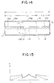
- FIG.14 shows a third embodiment of the present invention wherein the present invention is applied to the DFB laser diode that has three separated electrodes 15A, 15B and 15C instead of the single electrode 15 of the previous embodiments.
- Other parts of the laser diode is constructed substantially identical with the previous embodiments, for example the second embodiment. Thereby, the laser diode has the distribution of the linewidth enhancement factor ⁇ similar to FIG.7.
- FIG.15 shows the distribution profile of the refractive index n in the longitudinal direction of the laser diode.
- the change of the refractive index in the reverse direction in correspondence to the region 13B is effectively suppressed, and the laser diode shows a large shift of oscillation wavelength in response to the modulation of the injection current.
- the structure of the laser diode is not limited to those described.
- the waveguide layer 12 may be provided above the active layer 13 or 13′, with the corrugation grating 11a formed on the upper major surface of the waveguide layer 12.
- the substrate 11 may include one or more buffer layers for improvement of quality of the crystal of the active layer.
- the localized decrease of the parameter ⁇ may be achieved by forming the active layer by a single MQW structure and increasing the total thickness of the MQW structure in correspondence to the central region 13B similar to the case of FIG.13(D).
- the number of quantum wells included in the MQW structure is increased in the region 13B as compared with the regions 13A and 13C.
- the differential gain dG/dN increases in correspondence to the region 13B.
- one may form the active layer from a single MQW structure and erase the quantum well structure by implanting impurities such as Zn in correspondence to the regions 13A and 13C.
Landscapes
- Physics & Mathematics (AREA)
- Optics & Photonics (AREA)
- Condensed Matter Physics & Semiconductors (AREA)
- General Physics & Mathematics (AREA)
- Electromagnetism (AREA)
- Chemical & Material Sciences (AREA)
- Engineering & Computer Science (AREA)
- Nanotechnology (AREA)
- Life Sciences & Earth Sciences (AREA)
- Biophysics (AREA)
- Crystallography & Structural Chemistry (AREA)
- Semiconductor Lasers (AREA)
Applications Claiming Priority (2)
| Application Number | Priority Date | Filing Date | Title |
|---|---|---|---|
| JP3784591 | 1991-02-08 | ||
| JP37845/91 | 1991-02-08 |
Publications (2)
| Publication Number | Publication Date |
|---|---|
| EP0498736A2 true EP0498736A2 (fr) | 1992-08-12 |
| EP0498736A3 EP0498736A3 (en) | 1993-04-14 |
Family
ID=12508875
Family Applications (1)
| Application Number | Title | Priority Date | Filing Date |
|---|---|---|---|
| EP19920400328 Withdrawn EP0498736A3 (en) | 1991-02-08 | 1992-02-07 | Dfb laser diode having a modified profile of linewidth enhancement factor |
Country Status (1)
| Country | Link |
|---|---|
| EP (1) | EP0498736A3 (fr) |
Cited By (2)
| Publication number | Priority date | Publication date | Assignee | Title |
|---|---|---|---|---|
| US20210344172A1 (en) * | 2018-11-19 | 2021-11-04 | Mitsubishi Electric Corporation | Optical semiconductor device and method of manufacturing optical semiconductor device |
| EP4224645A4 (fr) * | 2020-10-26 | 2025-01-15 | Zhongxing Photonics Technology Co., Ltd. | Laser et son procédé de fabrication |
Family Cites Families (5)
| Publication number | Priority date | Publication date | Assignee | Title |
|---|---|---|---|---|
| JP2526898B2 (ja) * | 1987-05-08 | 1996-08-21 | 三菱電機株式会社 | 半導体レ−ザおよびその使用方法 |
| FR2639773B1 (fr) * | 1988-11-25 | 1994-05-13 | Alcatel Nv | Laser a semi-conducteur accordable |
| US5119393A (en) * | 1989-06-14 | 1992-06-02 | Hitachi, Ltd. | Semiconductor laser device capable of controlling wavelength shift |
| JP2890745B2 (ja) * | 1990-08-20 | 1999-05-17 | 富士通株式会社 | 半導体装置の製造方法および、光半導体装置の製造方法 |
| EP0487351B1 (fr) * | 1990-11-21 | 1995-07-12 | Kabushiki Kaisha Toshiba | Laser semi-conducteur accordable à rétroaction distribuée |
-
1992
- 1992-02-07 EP EP19920400328 patent/EP0498736A3/en not_active Withdrawn
Cited By (3)
| Publication number | Priority date | Publication date | Assignee | Title |
|---|---|---|---|---|
| US20210344172A1 (en) * | 2018-11-19 | 2021-11-04 | Mitsubishi Electric Corporation | Optical semiconductor device and method of manufacturing optical semiconductor device |
| US12199409B2 (en) * | 2018-11-19 | 2025-01-14 | Mitsubishi Electric Corporation | Optical semiconductor device and method of manufacturing optical semiconductor device |
| EP4224645A4 (fr) * | 2020-10-26 | 2025-01-15 | Zhongxing Photonics Technology Co., Ltd. | Laser et son procédé de fabrication |
Also Published As
| Publication number | Publication date |
|---|---|
| EP0498736A3 (en) | 1993-04-14 |
Similar Documents
| Publication | Publication Date | Title |
|---|---|---|
| US5459747A (en) | Semiconductor optical devices | |
| EP0472221B1 (fr) | Méthode pour la fabrication d'un dispositif optique à semi-conducteur | |
| US4728628A (en) | Method of making ridge waveguide lasers | |
| US5436195A (en) | Method of fabricating an integrated semiconductor light modulator and laser | |
| EP0375021B1 (fr) | Laser à diode semi-conductrice accordable à réflexion répartie et procédé de fabrication d'un tel laser à diode semi-conductrice | |
| US4426702A (en) | Semiconductor laser device | |
| JPS6215875A (ja) | 半導体装置およびその製造方法 | |
| EP0378098B1 (fr) | Dispositif optique à semi-conducteur | |
| EP0177221B1 (fr) | Laser à semi-conducteur | |
| US5847415A (en) | Light emitting device having current blocking structure | |
| EP0680119A1 (fr) | Procédé de fabrication d'un dispositif optique à semi-conducteur | |
| EP0527615A1 (fr) | Méthode pour la fabrication d'un laser à semi-conducteur accordable | |
| JP3204474B2 (ja) | 利得結合分布帰還型半導体レーザとその作製方法 | |
| EP0687938B1 (fr) | Dispositif optique à semi-conducteur utilisant un effet optique non-linéaire | |
| JP4097950B2 (ja) | 分布帰還型レーザ装置、半導体光装置および分布帰還型レーザ装置の製造方法 | |
| EP0498736A2 (fr) | Diode laser DFB avec profile modifié du paramètre alpha | |
| CN115336123A (zh) | 电吸收调制激光器 | |
| JPH0548214A (ja) | 分布反射型半導体レーザ | |
| US4894834A (en) | Semiconductor laser and method for production thereof | |
| JPH03151684A (ja) | 多波長集積化半導体レーザの製造方法 | |
| US5304507A (en) | Process for manufacturing semiconductor laser having low oscillation threshold current | |
| JPH08236857A (ja) | 長波長半導体レーザおよびその製造方法 | |
| JPH077232A (ja) | 光半導体装置 | |
| US5360763A (en) | Method for fabricating an optical semiconductor device | |
| JPH0462195B2 (fr) |
Legal Events
| Date | Code | Title | Description |
|---|---|---|---|
| PUAI | Public reference made under article 153(3) epc to a published international application that has entered the european phase |
Free format text: ORIGINAL CODE: 0009012 |
|
| AK | Designated contracting states |
Kind code of ref document: A2 Designated state(s): DE FR GB |
|
| PUAL | Search report despatched |
Free format text: ORIGINAL CODE: 0009013 |
|
| AK | Designated contracting states |
Kind code of ref document: A3 Designated state(s): DE FR GB |
|
| STAA | Information on the status of an ep patent application or granted ep patent |
Free format text: STATUS: THE APPLICATION IS DEEMED TO BE WITHDRAWN |
|
| 18D | Application deemed to be withdrawn |
Effective date: 19931015 |