EP0499225A2 - Dekodierungsvorrichtung für Kodes variabler Länge - Google Patents
Dekodierungsvorrichtung für Kodes variabler Länge Download PDFInfo
- Publication number
- EP0499225A2 EP0499225A2 EP92102320A EP92102320A EP0499225A2 EP 0499225 A2 EP0499225 A2 EP 0499225A2 EP 92102320 A EP92102320 A EP 92102320A EP 92102320 A EP92102320 A EP 92102320A EP 0499225 A2 EP0499225 A2 EP 0499225A2
- Authority
- EP
- European Patent Office
- Prior art keywords
- data
- shifted
- bit
- shifted number
- variable
- Prior art date
- Legal status (The legal status is an assumption and is not a legal conclusion. Google has not performed a legal analysis and makes no representation as to the accuracy of the status listed.)
- Granted
Links
Images




Classifications
-
- H—ELECTRICITY
- H03—ELECTRONIC CIRCUITRY
- H03M—CODING; DECODING; CODE CONVERSION IN GENERAL
- H03M7/00—Conversion of a code where information is represented by a given sequence or number of digits to a code where the same, similar or subset of information is represented by a different sequence or number of digits
- H03M7/30—Compression; Expansion; Suppression of unnecessary data, e.g. redundancy reduction
- H03M7/40—Conversion to or from variable length codes, e.g. Shannon-Fano code, Huffman code, Morse code
- H03M7/42—Conversion to or from variable length codes, e.g. Shannon-Fano code, Huffman code, Morse code using table look-up for the coding or decoding process, e.g. using read-only memory
- H03M7/425—Conversion to or from variable length codes, e.g. Shannon-Fano code, Huffman code, Morse code using table look-up for the coding or decoding process, e.g. using read-only memory for the decoding process only
Definitions
- the present invention generally relates to digital signal processing, and more particularly to a device for decoding a series signal including a plurality of data pieces described by codes having variable code lengths to reproduce the original equi-length codes.
- Variable-length coding is intended to enhance coding efficiency.
- the CCITT Recommendation H.261 defines a variable-length code.
- data pieces are described by equi-length code words.
- an event which frequently occurs is described by a short code word, and an event which does not frequently occur is described by a long code word.
- the average of the lengths of variable-length code words is smaller than the fixed length of equi-length code words.
- the variable-length coding as described above is widely used as an effective means for efficiently encoding video or image data.
- variable-length codes In a system capable of transmitting the variable-length codes, only effective data pieces which may have different lengths are successively transmitted. On the receiver side, the effective data pieces are decoded in a decoding unit which consists of a predetermined number of consecutive bits, the most significant bit of which is the beginning bit of each of the effective data pieces. In this manner, equi-length codes are reproduced.
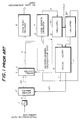
- FIG.1 is a block diagram of a conventional variable-length code decoding device.
- the device shown in FIG.1 is composed of a S/P (Serial to Parallel) converter 1, a buffer memory 2, a barrel shifter 3, a code word decoder 4, a code length detector 5, a code length register 61, a shifted-number register 62, and a MOD(N) adder 7.
- Serial data transmitted via a transmission path interface part (not shown) is sequentially converted into parallel data for every N bits or every N-bit group (for example, one byte), and then stored in the buffer memory 2.
- This buffer memory 2 always stores 2N-byte parallel data (two-byte parallel data) which consists of the previously received N-byte data and the N-byte data received at the present time.
- the buffer memory 2 always holds two bytes.
- the two-byte parallel data is always output from the buffer memory 2.
- the buffer memory 2 receives a carry signal from the adder 7, the contents of the buffer memory 2 are updated so that it stores the current (latest) one-byte data and the next one-byte data.
- the barrel shifter 3 which is controlled by a shifted number "j" (the number of bits to be shifted), is formed with a bit shifter, and always inputs the two-byte parallel data from the buffer memory 2.
- the barrel shifter 3 shifts the two-byte parallel data by the shifted number "j" in a high-order-bit direction, and outputs data consisting of eight consecutive bits, the beginning bit of which is the (j+1)th bit from the most significant bit of the received two-byte parallel data. In this manner, the beginning bit of the effective data which is about to be processed by the code word decoder 4 is placed at the most significant bit of the one-byte parallel data output by the barrel shifter 3.
- the code word decoder 4 is formed with a ROM (Read Only Memory), and receives, as an address signal, a bit pattern of the one-byte data output by the barrel shifter 3. A fixed-length code pattern specified by the bit pattern is read out from the code word decoder 4.
- the code length detector is formed with a ROM, which receives, as an address signal, the bit pattern output by the barrel shifter 3.
- the code length detector 5 stores various numbers of bits corresponding to various bit patterns. In response to the bit pattern from the barrel shifter 3, the number of bits (code length) which form the effective data from the barrel shifter 3 is output to the code length register 61.
- the effective data transmitted in the present system has a code length smaller than or equal to the number of bits N (one byte), and the last-bit position of the code is definitely determined by the pattern.
- the code-length data "m" output by the code length detector 5 is input to the adder 7 via the code length register 61.
- the register 62 holds the previous shifted number "j'", which is input to the adder 7.
- the adder 7 executes a MOD(N) addition operation on the code length "m” and the previous shifted number "j'". The result of this addition is the updated shifted number "j".
- the code-length data m read out from the code length detector 4 is input to the code length register 61.
- the previous shifted number "j'" output by the adder 7 is input to the register 62.
- Each of the registers 61 and 62 can be formed with a D-type flip-flop, which is driven by an operation clock signal CLK.
- the data m and j' are output from the registers 61 and 62, respectively, and input to the adder 7.
- the result of the MOD(N) addition operation, "j" is output by the adder 7.
- j is equal to j' + m. If the result shows the number of bits equal to or larger than N, j is equal to j' + m - N, and a carry signal CRY is made active (that is, shows "1"). Since the shifted number is changed from "j'" to "j", the barrel shifter 3 shifts the two-byte parallel data by j bits, and outputs the shifted bits after a predetermined operation delay timed ⁇ . When the carry signal CRY is generated, the input from the buffer memory 2 to the barrel shifter 3 is switched to 2N bits obtained by shifting the currently stored 2N bits by N bits in the high-order-bit direction.
- the barrel shifter 3 shifts the updated 2N bits by the shifted number "j" in the manner as described above. After a predetermined operation delay time ⁇ , the code length data "m" of the bit pattern output by the barrel shifter 3 is output by the code length detector 5.
- the above-mentioned decoding process should be carried out within one cycle of the operation clock signal CLK. It takes a time (delay time) ⁇ + ⁇ + ⁇ + ⁇ to calculate the shifted number "j" by a shifted number calculation loop. This delay time must be within one cycle of the operation clock signal CLK. Hence, the maximum frequency of the operation clock signal CLK is limited by the delay time necessary to obtain the shifted number "j".
- a more specific object of the present invention is to provide a variable-length code decoding device capable of calculating a shifted number at a higher speed.
- variable-length code decoding device comprising: converter means for converting serial data into parallel data for every N bits where N is an integer, the serial data including consecutive data pieces having variable data lengths; buffer memory means, coupled to the converter means, for storing the parallel data which is sequentially read out therefrom for every 2N bits and which is shifted by N bits in a high-order-bit direction in response to a carry signal; register means for storing a shifted number "j" which is read out therefrom in response to a clock signal, the shifted number "j” indicating the number of bits to be shifted; barrel shifter means, coupled to the buffer memory means, for receiving the parallel data from the buffer memory means and for shifting, by the shifted number "j", the parallel data in the high-order-bit direction so that N-bit parallel data having a starting bit which corresponds to an (j+1)th bit of the parallel data from a most significant bit thereof is output from the barrel shifter means; and shifted number/carry signal generator means, coupled to
- FIG.2 is a block diagram showing an outline of the present invention.
- a variable-length code decoding device shown in FIG.2 has a shifted number/carry signal generator 8 and a shifted number register 162, all of which are substituted for the code length detector 5, the adder 7, and the registers 61 and 62.
- the shifted number/carry signal generator 8 receives the previous shifted number "j'" read out from the register 162 and the N-bit data output by the barrel shifter 3, and generates an updated shifted number "j" and the carry signal CRY. In response to the clock signal CLK, the updated shifted number "j" is written into the register 162.
- the updated shifted number "j" is calculated on the basis of the code length of effective data contained in the N-bit data from the barrel shifter 3, and the previous shifted number "j'" read out from the register 162 so that the beginning bit of the next effective data is placed at the most significant bit of the one-byte bit pattern.
- the shifted number/carry signal generator 8 can be formed with a ROM. It is to be noted that it takes the sum of the delay times of the barrel shifter 3, the generator 8 and the register 162 to calculate the shifted number "j". Hence, the device shown in FIG.2 can operate at a speed higher than that of the device shown in FIG.1.
- FIG.3 is a block diagram of an embodiment of the present invention.
- the shifted number/carry signal generator 8 is formed with a ROM, which receives an address signal consisting of 11 bits a1 - a11, and four output bits d1 - d4.
- Eight high-order bits a11 - a4 of the address signal are eight bits output by the barrel shifter 3, and three low-order bits a3 - a1 thereof are three bits forming the previous shifted number "j'" read out from the register 162.
- Three high-order bits d4 - d2 show the current or updated shifted number "j" calculated based on the eight bits from the barrel shifter 3 and the three-bit previous shift register "j'".
- the ROM 8 stores all bit patterns consisting of bits d4 - d1 corresponding to all combinations of bits a11 - a1.
- the three high-order bits indicating the number of shifts "j" are stored in the register 162 and then input to the ROM 8, as the previous shifted number "j'".
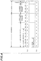
- FIG.4 is a diagram showing the contents of the ROM 8 which forms the shifted number/carry signal generator shown in FIG.2.
- the address of the ROM 8 obtained in this case is "000110XX011".
- the address of the ROM 8 obtained in this case is ")11XXXXX010".
- data "1010" which is calculated beforehand is stored.
- the sum of the effective data length "3" and the previous shifted number "2” is "5".
- the three high-order bits d4 -d2 are "101", and the carry signal CRY is made inactive ("0").
- the ROM 8 stores data (consisting of the shifted number and the carry signal) corresponding to all 11-bit address patterns.
- FIG.5 is a diagram showing how data is processed in the variable-length code decoding device shown in FIG.3.
- the barrel shifter 3 and the register 162 have the operation delay times ⁇ and ⁇ , respectively.
- the ROM 8 has an operation delay time ⁇ equal to that of the code length detector 5 formed with a ROM. Hence, it takes the total delay time ⁇ + ⁇ + ⁇ to obtain the shifted number "j". That is, the device shown in FIG.3 is faster than the conventional device shown in FIG.1 by the delay time ⁇ of the adder 7 shown in FIG.1. In addition, the device shown in FIG.3 can be made compact, as compared with the conventional device shown in FIG.1.
- the shifted number/carry signal generator 8 can be formed with another device in which one output pattern is specified by one input pattern.
- the generator 8 can be formed with a PLA (Programmable Logic Array).
- FIG.6 is a block diagram of a video codec to which the present invention is applied.
- the video codec (coder/decoder) shown in FIG.6 is composed of a transmission coder 21, a transmission buffer 22, a video signal multiplexing coder 23, an information source coder 24, a coding controller 25, a transmission decoder 26, a receiver buffer 27, a video signal multiplexing decoder 28 and an information source decoder 29.
- the receive buffer 27 corresponds to the aforementioned buffer memory 2
- the video signal multiplexing decoder 28 corresponds to the barrel shifter 3, the code word decoder 4, the ROM 8 and the register 162.
Landscapes
- Engineering & Computer Science (AREA)
- Theoretical Computer Science (AREA)
- Compression, Expansion, Code Conversion, And Decoders (AREA)
Applications Claiming Priority (2)
| Application Number | Priority Date | Filing Date | Title |
|---|---|---|---|
| JP3019691A JP3063180B2 (ja) | 1991-02-13 | 1991-02-13 | 可変長符号復号回路 |
| JP19691/91 | 1991-02-13 |
Publications (3)
| Publication Number | Publication Date |
|---|---|
| EP0499225A2 true EP0499225A2 (de) | 1992-08-19 |
| EP0499225A3 EP0499225A3 (en) | 1992-11-25 |
| EP0499225B1 EP0499225B1 (de) | 1997-05-07 |
Family
ID=12006274
Family Applications (1)
| Application Number | Title | Priority Date | Filing Date |
|---|---|---|---|
| EP19920102320 Expired - Lifetime EP0499225B1 (de) | 1991-02-13 | 1992-02-12 | Dekodierungsvorrichtung für Kodes variabler Länge |
Country Status (3)
| Country | Link |
|---|---|
| EP (1) | EP0499225B1 (de) |
| JP (1) | JP3063180B2 (de) |
| DE (1) | DE69219494T2 (de) |
Cited By (2)
| Publication number | Priority date | Publication date | Assignee | Title |
|---|---|---|---|---|
| GB2269070B (en) * | 1992-07-07 | 1996-04-24 | Ricoh Kk | Huffman decoder architecture for high speed operation and reduced memory |
| EP0769852A1 (de) * | 1995-10-19 | 1997-04-23 | Samsung Electronics Co., Ltd. | Dekodierer variabler Länge unter Verwendung eines FIFO-Speichers |
Families Citing this family (1)
| Publication number | Priority date | Publication date | Assignee | Title |
|---|---|---|---|---|
| WO1994024672A1 (fr) * | 1993-04-19 | 1994-10-27 | Oki Electric Industry Co., Ltd. | Circuit pour le decodage de codes de longueur variable, et systeme pour le decodage de codes de longueur variable qui utilise ce circuit |
Family Cites Families (1)
| Publication number | Priority date | Publication date | Assignee | Title |
|---|---|---|---|---|
| US3918047A (en) * | 1974-03-28 | 1975-11-04 | Bell Telephone Labor Inc | Decoding circuit for variable length codes |
-
1991
- 1991-02-13 JP JP3019691A patent/JP3063180B2/ja not_active Expired - Lifetime
-
1992
- 1992-02-12 DE DE1992619494 patent/DE69219494T2/de not_active Expired - Fee Related
- 1992-02-12 EP EP19920102320 patent/EP0499225B1/de not_active Expired - Lifetime
Cited By (3)
| Publication number | Priority date | Publication date | Assignee | Title |
|---|---|---|---|---|
| GB2269070B (en) * | 1992-07-07 | 1996-04-24 | Ricoh Kk | Huffman decoder architecture for high speed operation and reduced memory |
| EP0769852A1 (de) * | 1995-10-19 | 1997-04-23 | Samsung Electronics Co., Ltd. | Dekodierer variabler Länge unter Verwendung eines FIFO-Speichers |
| US5892791A (en) * | 1995-10-19 | 1999-04-06 | Samsung Electronics Co., Ltd. | High-speed variable length decoding apparatus |
Also Published As
| Publication number | Publication date |
|---|---|
| EP0499225B1 (de) | 1997-05-07 |
| JPH04258025A (ja) | 1992-09-14 |
| EP0499225A3 (en) | 1992-11-25 |
| DE69219494T2 (de) | 1997-09-25 |
| DE69219494D1 (de) | 1997-06-12 |
| JP3063180B2 (ja) | 2000-07-12 |
Similar Documents
| Publication | Publication Date | Title |
|---|---|---|
| US5696507A (en) | Method and apparatus for decoding variable length code | |
| US5436626A (en) | Variable-length codeword encoder | |
| JP2915568B2 (ja) | テープドライブシステムのための適応データ圧縮装置 | |
| US4989000A (en) | Data string compression using arithmetic encoding with simplified probability subinterval estimation | |
| US4376933A (en) | Circuit for compacting data | |
| KR0185592B1 (ko) | 가변 길이 데이타의 부호화 및 복호장치 | |
| US5309156A (en) | Variable-length code decoding device | |
| US5428627A (en) | Method and apparatus for initializing an ECC circuit | |
| JP3231855B2 (ja) | データフォーマット変換装置及び方法 | |
| JP3294026B2 (ja) | 高速可変長復号化装置 | |
| US4327379A (en) | Hardware implementation of 4-pixel code encoder | |
| US4494151A (en) | 4-Pixel run-length code for data compression | |
| JPH0916373A (ja) | 可変長コードの符号化及び分割装置 | |
| US6301389B1 (en) | Video image color encoding | |
| KR0178201B1 (ko) | 가변 길이 복호화 장치 | |
| JP2000261674A (ja) | 画像伸長装置 | |
| JP2922571B2 (ja) | データ変換回路 | |
| JPH03503707A (ja) | 統計的にコード化されたデジタル・データを復号するシステム | |
| GB2333000A (en) | Finite state machine coding of information | |
| US5067023A (en) | Image data coding apparatus | |
| EP0149893B1 (de) | Apparat zum Kodieren und Dekodieren von Daten | |
| EP0499225B1 (de) | Dekodierungsvorrichtung für Kodes variabler Länge | |
| KR100207385B1 (ko) | 가변 길이 복호화 장치 | |
| US4499498A (en) | Run length decoding apparatus | |
| US5694126A (en) | Adaptive predictive data compression method and apparatus |
Legal Events
| Date | Code | Title | Description |
|---|---|---|---|
| PUAI | Public reference made under article 153(3) epc to a published international application that has entered the european phase |
Free format text: ORIGINAL CODE: 0009012 |
|
| AK | Designated contracting states |
Kind code of ref document: A2 Designated state(s): DE FR GB |
|
| PUAL | Search report despatched |
Free format text: ORIGINAL CODE: 0009013 |
|
| AK | Designated contracting states |
Kind code of ref document: A3 Designated state(s): DE FR GB |
|
| 17P | Request for examination filed |
Effective date: 19921209 |
|
| 17Q | First examination report despatched |
Effective date: 19950502 |
|
| GRAG | Despatch of communication of intention to grant |
Free format text: ORIGINAL CODE: EPIDOS AGRA |
|
| GRAH | Despatch of communication of intention to grant a patent |
Free format text: ORIGINAL CODE: EPIDOS IGRA |
|
| GRAH | Despatch of communication of intention to grant a patent |
Free format text: ORIGINAL CODE: EPIDOS IGRA |
|
| GRAA | (expected) grant |
Free format text: ORIGINAL CODE: 0009210 |
|
| AK | Designated contracting states |
Kind code of ref document: B1 Designated state(s): DE FR GB |
|
| PG25 | Lapsed in a contracting state [announced via postgrant information from national office to epo] |
Ref country code: FR Effective date: 19970507 |
|
| REF | Corresponds to: |
Ref document number: 69219494 Country of ref document: DE Date of ref document: 19970612 |
|
| EN | Fr: translation not filed | ||
| PLBE | No opposition filed within time limit |
Free format text: ORIGINAL CODE: 0009261 |
|
| STAA | Information on the status of an ep patent application or granted ep patent |
Free format text: STATUS: NO OPPOSITION FILED WITHIN TIME LIMIT |
|
| 26N | No opposition filed | ||
| PGFP | Annual fee paid to national office [announced via postgrant information from national office to epo] |
Ref country code: DE Payment date: 19991231 Year of fee payment: 9 |
|
| PGFP | Annual fee paid to national office [announced via postgrant information from national office to epo] |
Ref country code: GB Payment date: 20000209 Year of fee payment: 9 |
|
| PG25 | Lapsed in a contracting state [announced via postgrant information from national office to epo] |
Ref country code: GB Free format text: LAPSE BECAUSE OF NON-PAYMENT OF DUE FEES Effective date: 20010212 |
|
| GBPC | Gb: european patent ceased through non-payment of renewal fee |
Effective date: 20010212 |
|
| PG25 | Lapsed in a contracting state [announced via postgrant information from national office to epo] |
Ref country code: DE Free format text: LAPSE BECAUSE OF NON-PAYMENT OF DUE FEES Effective date: 20011201 |