EP0499454A2 - Circuit automatique limiteur de luminosité - Google Patents
Circuit automatique limiteur de luminosité Download PDFInfo
- Publication number
- EP0499454A2 EP0499454A2 EP92301153A EP92301153A EP0499454A2 EP 0499454 A2 EP0499454 A2 EP 0499454A2 EP 92301153 A EP92301153 A EP 92301153A EP 92301153 A EP92301153 A EP 92301153A EP 0499454 A2 EP0499454 A2 EP 0499454A2
- Authority
- EP
- European Patent Office
- Prior art keywords
- abl
- voltage
- display units
- offset
- lowest
- Prior art date
- Legal status (The legal status is an assumption and is not a legal conclusion. Google has not performed a legal analysis and makes no representation as to the accuracy of the status listed.)
- Granted
Links
Images



Classifications
-
- H—ELECTRICITY
- H04—ELECTRIC COMMUNICATION TECHNIQUE
- H04N—PICTORIAL COMMUNICATION, e.g. TELEVISION
- H04N5/00—Details of television systems
- H04N5/44—Receiver circuitry for the reception of television signals according to analogue transmission standards
- H04N5/57—Control of contrast or brightness
-
- H—ELECTRICITY
- H04—ELECTRIC COMMUNICATION TECHNIQUE
- H04N—PICTORIAL COMMUNICATION, e.g. TELEVISION
- H04N9/00—Details of colour television systems
- H04N9/12—Picture reproducers
Definitions
- the present invention relates to a display apparatus in which a large multi-screen is constituted by a plurality of display units such as projection TVs. More particularly, the invention is directed to an ABL (Automatic Brightness Limiter) circuit which automatically adjusts brightness or contrast of a picture displayed on each display unit.
- ABL Automatic Brightness Limiter
- a large screen is formed by a plurality of display units U1-U9 arranged, e.g., in matrix form, and an enlarged single picture is displayed over the entire screen or different pictures are displayed on the respective display units U1-U9.
- Each of the display units U1-U9 has projectors for emitting three light beams corresponding to respective color video signals of R, G and B.
- the three light beams are projected onto a projection screen using, e.g., a Fresnel lens, to reproduce a picture.
- an ABL circuit is provided in each of the display units U1-U9.
- this conventional video display circuit operates so as to forcibly provide the common ABL signal, there is a possibility that the screens of some display units become too dark. This is explained more specifically.
- the minimum ABL voltage among the ABL voltages of the display units U1-U9 is employed as the common ABL signal. Therefore, while the brightness limitation is properly effected in the display units having ABL voltages close to the minimum ABL voltage, the brightness remains dark in the display units having higher ABL voltages.
- An object of the present invention is to provide an ABL circuit which can adjust the brightness and/or contrast of a plurality of display units constituting a multi-screen display apparatus so as to provide uniform brightness over the entire multi-screen.
- an automatic brightness limiter circuit for use in each of a plurality of display units constituting a multi-screen display apparatus having a lowest ABL level priority circuit which provides a lowest ABL voltage receiving ABL voltages from the plurality of display units, comprises: means for producing an ABL voltage which reflects brightness of a display unit having said automatic brightness control circuit; means for storing offset data corresponding to a difference of the ABL voltage of the display unit and a minimum ABL voltage among ABL voltages of the plurality of display units when the plurality of display units are adjusted to exhibit same brightness while receiving a same video signal; means for producing an offset voltage based on the offset data; means for receiving the lowest ABL voltage from the lowest ABL level priority circuit; and means for adding the offset voltage to the lowest ABL voltage to produce an offset-added ABL voltage to be used for adjusting brightness and/or contrast of the display unit.
- a method of adjusting brightness and/or contrast of a plurality of display units constituting a multi-screen display apparatus having a lowest ABL level priority circuit which provides a lowest ABL voltage receiving ABL voltages from the plurality of display units comprises the steps of: supplying a same video signal to the plurality of display units; determining and storing offset data of each of the plurality of display units, the offset data corresponding to a difference between an ABL voltage of each display unit and a minimum ABL voltage among ABL voltages of the plurality of display units when the plurality of display units are adjusted to exhibit same brightness; producing, in each display unit, an offset-added ABL voltage by adding an offset voltage produced based on the stored offset data to the lowest ABL voltage provided from the lowest ABL level priority circuit; and adjusting brightness and/or contrast of the plurality of display units based on the offset-added ABL voltages.
- FIG. 1 shows a basic construction of an ABL circuit according to an embodiment of the invention, which is incorporated in each of display units U1, U2, etc. constituting a display apparatus.
- the display unit U1 includes: an ABL signal detection means 2-1 for detecting an ABL signal sent from a flyback transformer 16-1; a buffer 3-1 for preventing reverse flow of an ABL voltage from the other display units U2 etc. to the ABL signal detection means 2-1 via an external connection terminal 6-1; a manually adjustable variable offset voltage generating means 5-1 for generating an offset voltage for the display unit U1; and an offset voltage adding means 4-1 for adding the offset voltage from the variable offset voltage generating means 5-1 to an ABL voltage sent from the buffer 3-1 or externally provided via the terminal 6-1.
- a resulting offset-added ABL voltage is provided to a video amplifying circuit 18-1.
- the display unit U1 further includes a CRT and TV circuits such as a brightness adjusting circuit and a synchronizing circuit, these components are not directly relevant to the invention and a description for those is therefore omitted.
- the other display units U2 etc. have the same construction.
- connection cable 7 which is connected to a lowest ABL level priority circuit such as a video display circuit disclosed in above-mentioned Japanese Utility Model Application Unexamined Publication No. Sho. 63-55683, which is hereby incorporated by reference for a more detailed understanding of the lowest ABL level priority circuit.
- a common, i.e., smallest ABL signal is supplied from the lowest ABL level priority circuit to each of the display units U1, U2, etc.
- the same video signal is supplied to each of the display units U1, U2, etc. to display a white picture on each display unit.
- a person in charge of the adjustment while observing the screens of the display units U1, U2, etc., operates the variable offset voltage generating means 5-1 of, e.g., the display unit U1 to apply an appropriate offset voltage to the offset voltage adding means 4-1 so that the brightness of the display unit U1 becomes equal to the display unit producing the minimum ABL voltage.
- the offset voltage adding means 4-1 adds the offset voltage output from the variable offset voltage generating means 5-1 to the ABL voltage output from the ABL signal detection means 2-1, and the resulting offset-added ABL voltage is provided to the video amplifying circuit 18-1.
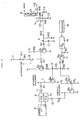
- FIG. 2 shows a specific circuit of the ABL circuit according to the embodiment, which is employed in all the display units U1, U2, etc.
- the display unit U1 which has a relationship a between the ABL voltage V ABL (a voltage at point C in fig. 2) and screen brightness, exhibits a brightness ⁇ at an ABL voltage V ABL of 4 V.
- the lowest ABL level priority circuit operates to restrict the ABL voltage of the display unit U2, which has a V ABL -screen brightness characteristic b , to 4 V, thereby setting the brightness of the display unit U2 to ⁇ .
- the ABL voltage of the display unit U2 should be increased to 6 V, requiring an offset voltage of 2 V ( 6 V - 4 V).
- each offset voltage is stored in a memory of a built-in controller 15 of the individual display unit.
- the offset data which corresponds to 2 V in the above example, is output from the controller 15.
- the offset data is converted to an analog voltage by a D/A converter 14, and then applied to the base of a transistor Q3.
- the transistor Q3 acts to increase a voltage at point B in accordance with the received offset voltage, and the increased voltage at point B in turn increases a voltage at point C via a transistor Q4, making the screen brighter.
- the brightness of the display unit U2 is increased, i.e., equated to the brightness of the display unit U1.
- the lowest ABL signal is provided via a line 7 and a terminal 6-1.
- a switch 13 is kept open during the presetting of the offset voltage, and is kept closed during the usual operation.
- Transistors Q1, Q2 constitute not only part of the lowest ABL level priority circuit, but also the buffer 3-1.
- a current flows from a voltage supply V1 through the transistor Q2 and resistors R4, R5 and R6, and a voltage at point B is changed in accordance with the base voltage of the transistor Q2.
- the lowest ABL voltage is also applied to the collector of the transistor Q1. If the subject display unit U1 exhibits a brighter picture, a voltage at point A is high and so the transistor Q1 is close to an off state. Therefore, the current through the transistor Q2 is determined by the lowest ABL signal rather than the voltage at point A.
- Microcomputers are incorporated in the respective display units U1, U2, etc. and interconnected via data lines.
- the microcomputer controls the switch 13. Further, detecting the ABL voltage at the time of the presetting, the microcomputer controls the controller 15 to store the offset data that corresponds to the difference between the detected ABL voltage of the subject display unit (U1) and the ABL voltage of the display unit producing the minimum ABL voltage.
- Capacitors C1, C2, a diode D, resistors R12, R13, R14, a capacitor C3, and other elements constitute a filter for the ABL signal detection and a clamp circuit which clamps the voltage at point A so that it does not exceeds the voltage V1.
- Resistors R5, R6, R8, R10, the transistor Q3 correspond to the offset voltage adding means 4-1.
- the controller 15 and the D/A converter 14 correspond to the variable offset voltage generating means 5-1.
- R16 designates an ABL signal detection resistor and thus corresponds to the ABL signal detection means 2-1.
- a controller 8 D/A converters 9, 10, buffers 11, 12, resistors R1, R2, R3, transistors Q4, Q5, Q6 constitute a brightness/contrast adjusting means.
- An operating unit (not shown) having a brightness button, a contrast button, etc. is connected to the controller 8.
- the controller 8 operates to adjust the brightness and contrast levels in accordance with a viewer's instruction that is input through the operating unit.
- the contrast adjustment by the transistors Q5, Q6 may similarly be performed by controlling, via the transistor Q3, the base voltage of the transistor Q5 in accordance with the offset data output from the controller 15.
Landscapes
- Engineering & Computer Science (AREA)
- Multimedia (AREA)
- Signal Processing (AREA)
- Television Receiver Circuits (AREA)
- Transforming Electric Information Into Light Information (AREA)
- Studio Circuits (AREA)
- Processing Of Color Television Signals (AREA)
- Controls And Circuits For Display Device (AREA)
- Control Of Indicators Other Than Cathode Ray Tubes (AREA)
Applications Claiming Priority (2)
| Application Number | Priority Date | Filing Date | Title |
|---|---|---|---|
| JP03041183A JP3140069B2 (ja) | 1991-02-12 | 1991-02-12 | 表示装置 |
| JP41183/91 | 1991-02-12 |
Publications (3)
| Publication Number | Publication Date |
|---|---|
| EP0499454A2 true EP0499454A2 (fr) | 1992-08-19 |
| EP0499454A3 EP0499454A3 (en) | 1992-10-14 |
| EP0499454B1 EP0499454B1 (fr) | 1996-04-10 |
Family
ID=12601308
Family Applications (1)
| Application Number | Title | Priority Date | Filing Date |
|---|---|---|---|
| EP92301153A Expired - Lifetime EP0499454B1 (fr) | 1991-02-12 | 1992-02-12 | Circuit automatique limiteur de luminosité |
Country Status (4)
| Country | Link |
|---|---|
| US (1) | US5231496A (fr) |
| EP (1) | EP0499454B1 (fr) |
| JP (1) | JP3140069B2 (fr) |
| DE (1) | DE69209691T2 (fr) |
Cited By (3)
| Publication number | Priority date | Publication date | Assignee | Title |
|---|---|---|---|---|
| DE19800846A1 (de) * | 1998-01-13 | 1999-07-22 | Grundig Ag | Vorrichtung zur Vermeidung einer Überhitzung eines Displaytreiber-Bausteins eines Plasmadisplays |
| DE19832261A1 (de) * | 1998-07-17 | 2000-01-20 | Thomson Brandt Gmbh | Anordnung zur Regelung der Luminanz |
| CN105308671A (zh) * | 2013-06-14 | 2016-02-03 | Eizo株式会社 | 多监视器系统、多监视器系统所使用的计算机程序及显示装置 |
Families Citing this family (3)
| Publication number | Priority date | Publication date | Assignee | Title |
|---|---|---|---|---|
| KR0147862B1 (ko) * | 1994-08-25 | 1998-09-15 | 김광호 | 다중모드 모니터의 자동 빔전류 조성회로 및 그 방법 |
| KR100330172B1 (ko) * | 1999-07-29 | 2002-03-28 | 윤종용 | Lcd프로젝션시스템의 명암대비개선장치 |
| TWI286440B (en) * | 2005-06-27 | 2007-09-01 | Benq Corp | Cathode ray tube display, device and method for controlling brightness thereof |
Family Cites Families (6)
| Publication number | Priority date | Publication date | Assignee | Title |
|---|---|---|---|---|
| DE3222266A1 (de) * | 1982-06-10 | 1983-12-15 | Karl Heinz 2000 Hamburg Krings | Demonstrationswand |
| JPS6043981A (ja) * | 1983-08-22 | 1985-03-08 | Sony Corp | ビ−ム電流制限回路 |
| JPS6276980A (ja) * | 1985-09-30 | 1987-04-09 | Matsushita Electric Ind Co Ltd | 平板形陰極線管の駆動方法 |
| US4746981A (en) * | 1986-06-16 | 1988-05-24 | Imtech International, Inc. | Multiple screen digital video display |
| JPH0520069Y2 (fr) * | 1986-09-27 | 1993-05-26 | ||
| US4901156A (en) * | 1986-12-26 | 1990-02-13 | Goldstart Co., Ltd. | Automatic brightness limiting circuit |
-
1991
- 1991-02-12 JP JP03041183A patent/JP3140069B2/ja not_active Expired - Fee Related
-
1992
- 1992-02-11 US US07/833,518 patent/US5231496A/en not_active Expired - Lifetime
- 1992-02-12 DE DE69209691T patent/DE69209691T2/de not_active Expired - Fee Related
- 1992-02-12 EP EP92301153A patent/EP0499454B1/fr not_active Expired - Lifetime
Cited By (4)
| Publication number | Priority date | Publication date | Assignee | Title |
|---|---|---|---|---|
| DE19800846A1 (de) * | 1998-01-13 | 1999-07-22 | Grundig Ag | Vorrichtung zur Vermeidung einer Überhitzung eines Displaytreiber-Bausteins eines Plasmadisplays |
| DE19800846C2 (de) * | 1998-01-13 | 1999-12-09 | Grundig Ag | Vorrichtung zur Vermeidung einer Überhitzung eines Displaytreiber-Bausteins eines Plasmadisplays |
| DE19832261A1 (de) * | 1998-07-17 | 2000-01-20 | Thomson Brandt Gmbh | Anordnung zur Regelung der Luminanz |
| CN105308671A (zh) * | 2013-06-14 | 2016-02-03 | Eizo株式会社 | 多监视器系统、多监视器系统所使用的计算机程序及显示装置 |
Also Published As
| Publication number | Publication date |
|---|---|
| EP0499454B1 (fr) | 1996-04-10 |
| EP0499454A3 (en) | 1992-10-14 |
| US5231496A (en) | 1993-07-27 |
| JP3140069B2 (ja) | 2001-03-05 |
| JPH04257890A (ja) | 1992-09-14 |
| DE69209691D1 (de) | 1996-05-15 |
| DE69209691T2 (de) | 1996-10-31 |
Similar Documents
| Publication | Publication Date | Title |
|---|---|---|
| US6882363B1 (en) | Video signal processing apparatus | |
| JPS61269484A (ja) | カラ−ビデオカメラの自動ホワイトバランス調整装置 | |
| EP0499454B1 (fr) | Circuit automatique limiteur de luminosité | |
| JPS60167590A (ja) | 撮像装置 | |
| JPH03230698A (ja) | オートホワイトバランス調整装置 | |
| JPS62189450A (ja) | 電子プリンタおよびその画像輝度調節方法 | |
| EP0841809A2 (fr) | Dispositif de stabilisation automatique du niveau de noir | |
| JPS63227285A (ja) | 映像信号制御装置 | |
| JPS5850867A (ja) | Cctvカメラ用自動絞り制御装置 | |
| JPS6064580A (ja) | Cctvカメラ用レンズの自動絞り制御装置 | |
| JP2588696B2 (ja) | 自動露出補正装置 | |
| JPH0258834B2 (fr) | ||
| JPH02272892A (ja) | ホワイトバランス制御装置 | |
| JPS6180988A (ja) | カラ−ビデオカメラにおける自動ホワイトバランス調整装置 | |
| KR100215427B1 (ko) | 셔터모드에따른비데오신호의레벨조정방법및그장치 | |
| KR100242609B1 (ko) | 카메라의 영상데이타 출력제어장치 및 그 방법 | |
| JPH0410784B2 (fr) | ||
| JPH06197268A (ja) | 逆光補正機能付きビデオカメラ | |
| JP2521833Y2 (ja) | 映像撮像装置の焦点深度自動調節回路 | |
| JPH01256281A (ja) | オートマスタペデスタル調整回路 | |
| KR19990030441U (ko) | 디스플레이장치의 화면밝기 조정장치 | |
| JPH09331537A (ja) | 撮像装置 | |
| KR940004972Y1 (ko) | 비디오 카메라의 색필터 선택회로 | |
| JP2823183B2 (ja) | ビデオカメラ | |
| JPS5943872B2 (ja) | カラ−撮像装置 |
Legal Events
| Date | Code | Title | Description |
|---|---|---|---|
| PUAI | Public reference made under article 153(3) epc to a published international application that has entered the european phase |
Free format text: ORIGINAL CODE: 0009012 |
|
| AK | Designated contracting states |
Kind code of ref document: A2 Designated state(s): DE FR GB |
|
| PUAL | Search report despatched |
Free format text: ORIGINAL CODE: 0009013 |
|
| AK | Designated contracting states |
Kind code of ref document: A3 Designated state(s): DE FR GB |
|
| 17P | Request for examination filed |
Effective date: 19930325 |
|
| 17Q | First examination report despatched |
Effective date: 19950504 |
|
| GRAA | (expected) grant |
Free format text: ORIGINAL CODE: 0009210 |
|
| AK | Designated contracting states |
Kind code of ref document: B1 Designated state(s): DE FR GB |
|
| REF | Corresponds to: |
Ref document number: 69209691 Country of ref document: DE Date of ref document: 19960515 |
|
| ET | Fr: translation filed | ||
| PLBE | No opposition filed within time limit |
Free format text: ORIGINAL CODE: 0009261 |
|
| 26N | No opposition filed | ||
| REG | Reference to a national code |
Ref country code: GB Ref legal event code: 746 Effective date: 19980115 |
|
| REG | Reference to a national code |
Ref country code: FR Ref legal event code: D6 |
|
| PGFP | Annual fee paid to national office [announced via postgrant information from national office to epo] |
Ref country code: DE Payment date: 20010205 Year of fee payment: 10 |
|
| PGFP | Annual fee paid to national office [announced via postgrant information from national office to epo] |
Ref country code: GB Payment date: 20010207 Year of fee payment: 10 |
|
| PGFP | Annual fee paid to national office [announced via postgrant information from national office to epo] |
Ref country code: FR Payment date: 20010213 Year of fee payment: 10 |
|
| REG | Reference to a national code |
Ref country code: GB Ref legal event code: IF02 |
|
| PG25 | Lapsed in a contracting state [announced via postgrant information from national office to epo] |
Ref country code: GB Free format text: LAPSE BECAUSE OF NON-PAYMENT OF DUE FEES Effective date: 20020212 |
|
| PG25 | Lapsed in a contracting state [announced via postgrant information from national office to epo] |
Ref country code: DE Free format text: LAPSE BECAUSE OF NON-PAYMENT OF DUE FEES Effective date: 20020903 |
|
| GBPC | Gb: european patent ceased through non-payment of renewal fee |
Effective date: 20020212 |
|
| PG25 | Lapsed in a contracting state [announced via postgrant information from national office to epo] |
Ref country code: FR Free format text: LAPSE BECAUSE OF NON-PAYMENT OF DUE FEES Effective date: 20021031 |
|
| REG | Reference to a national code |
Ref country code: FR Ref legal event code: ST |