EP0499824A1 - Cellule SRAM à capacité superposée - Google Patents
Cellule SRAM à capacité superposée Download PDFInfo
- Publication number
- EP0499824A1 EP0499824A1 EP92101131A EP92101131A EP0499824A1 EP 0499824 A1 EP0499824 A1 EP 0499824A1 EP 92101131 A EP92101131 A EP 92101131A EP 92101131 A EP92101131 A EP 92101131A EP 0499824 A1 EP0499824 A1 EP 0499824A1
- Authority
- EP
- European Patent Office
- Prior art keywords
- gate
- over
- transistors
- cell
- capacitor plates
- Prior art date
- Legal status (The legal status is an assumption and is not a legal conclusion. Google has not performed a legal analysis and makes no representation as to the accuracy of the status listed.)
- Granted
Links
Images
Classifications
-
- G—PHYSICS
- G11—INFORMATION STORAGE
- G11C—STATIC STORES
- G11C11/00—Digital stores characterised by the use of particular electric or magnetic storage elements; Storage elements therefor
- G11C11/21—Digital stores characterised by the use of particular electric or magnetic storage elements; Storage elements therefor using electric elements
- G11C11/34—Digital stores characterised by the use of particular electric or magnetic storage elements; Storage elements therefor using electric elements using semiconductor devices
- G11C11/40—Digital stores characterised by the use of particular electric or magnetic storage elements; Storage elements therefor using electric elements using semiconductor devices using transistors
- G11C11/41—Digital stores characterised by the use of particular electric or magnetic storage elements; Storage elements therefor using electric elements using semiconductor devices using transistors forming static cells with positive feedback, i.e. cells not needing refreshing or charge regeneration, e.g. bistable multivibrator or Schmitt trigger
- G11C11/412—Digital stores characterised by the use of particular electric or magnetic storage elements; Storage elements therefor using electric elements using semiconductor devices using transistors forming static cells with positive feedback, i.e. cells not needing refreshing or charge regeneration, e.g. bistable multivibrator or Schmitt trigger using field-effect transistors only
- G11C11/4125—Cells incorporating circuit means for protecting against loss of information
-
- H—ELECTRICITY
- H10—SEMICONDUCTOR DEVICES; ELECTRIC SOLID-STATE DEVICES NOT OTHERWISE PROVIDED FOR
- H10B—ELECTRONIC MEMORY DEVICES
- H10B10/00—Static random access memory [SRAM] devices
- H10B10/12—Static random access memory [SRAM] devices comprising a MOSFET load element
Definitions
- This invention generally relates to semiconductor fabrication methods and devices, and more specifically to static random access memory (SRAM) cell fabrication methods and devices.
- SRAM static random access memory
- CMOS inverters which is similar to an NMOS cell but with the load transistors in the NMOS cell replaced with PMOS transistors.
- the CMOS cell will require more area but the power consumption when the circuit is quiescent will be virtually eliminated.
- One method to improve the packing density of CMOS SRAMs is to stack the transistors one on top of another. This arrangement allows the circuit design to extend into the third dimension.
- the cell comprises: two NMOS drive transistors; two PMOS load transistors; first and second bottom capacitor plates, with the first plate being over a gate of one of the drive transistors and the second plate being over a gate of another of the drive transistors; a layer of dielectric material over the first and second bottom capacitor plates; and first and second top capacitor plates over the dielectric layer, with the first top capacitor plate forming a gate of one of the load transistors and with the second top capacitor plate forming a gate of another of the load transistors, whereby the capacitor plates form two cross-coupled capacitors between the gates of the drive transistors and the stability of the cell is enhanced.
- the dielectric material is oxide, nitride, tantalum oxide, or oxide and nitride.
- the method comprises: forming a first bottom capacitor plate over a gate of the second drive transistor and second bottom capacitor plate over a gate of the first drive transistor; electrically connecting the first bottom capacitor plate to the second drive transistors gate; electrically connecting the second bottom capacitor plate to the first drive transistor gate; forming dielectric layer over the first and second bottom capacitor plates; forming first and second top capacitor plates over the dielectric layer, with the first top capacitor plate forming a gate of the first load transistor and being over the first bottom capacitor plate, and the second top capacitor plate forming a gate of the second load transistor and being over the second bottom capacitor plate; electrically connecting the first top capacitor plate to the first drive transistor gate; electrically connecting the second top capacitor plate to the second drive transistor gate; and forming PMOS channel films over the first and second top capacitor plates.
- the first and second bottom capacitor plates are fabricated from silicon; the first and second top capacitor plates are fabricated from silicon; the first and second bottom capacitor plates are over gate sidewalls of the drive transistors; the first and second top capacitor plates are over gate sidewalls of the drive transistors; and the dielectric layer is oxide, nitride, tantalum oxide, or oxide and nitride.
- SER soft error rate
- SRAM cells have been designed, using PMOS transistors stacked atop NMOS transistors, which increases such cross-coupling.
- this coupling capacitance is substantially larger than in previous SRAM cells if the effective area of elements (which contribute that capacitance) is increased (previously, the PMOS transistors were stacked, but conventional element sizes were used).
- the intent of this embodiment is to increase the aforementioned capacitance by such increases in effective area (and possibly, changes in the dielectric between such elements).
- the addition of capacitor plates is a practical way to increase the effective area.
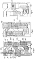
- FIGS. 1a-1c A preferred embodiment of the present invention is shown, in FIGS. 1a-1c, during sequential processing steps.
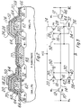
- FIG. 2 shows A cross-section (FIG. 2) and a schematic (FIG. 3) of this preferred embodiment are provided for clarification, and should be referred to when examining FIGS. 1a-1c.
- Table 1 below may also be used as a reference for the drawings.
- FIG. 1a shows the layout after formation of standard CMOS or BiCMOS well 48, formation of active regions (which includes the moat regions), the formation of drive transistor (DN3, DN4) gate regions 34,40, the formation of the access/transfer transistors (TN1, TN2) gate region 12, and the formation of gate to moat interconnects 16,30.
- CMOS or BiCMOS well 48 shows the layout after formation of standard CMOS or BiCMOS well 48, formation of active regions (which includes the moat regions), the formation of drive transistor (DN3, DN4) gate regions 34,40, the formation of the access/transfer transistors (TN1,
- the moat regions form the source 10 and drain 14 of TN1, the source 46 and drain 44 of TN2, the source 36 and drain 32 of DN4 and the source 38 and drain 42 of DN3.
- the interconnect is shown as a single mask process (e.g. using selective epitaxial silicon as an interconnect), however, a different method may be utilized.
- the source/drain regions and gate layer are n+ in doping and all transistors shown are fabricated in bulk silicon.
- the gates, moats, and interconnects may or may not be silicided depending on the choice of device technology. All of these regions can be seen in the schematic of FIG. 3., and the cross-sections of DN3 and DN4 are shown in FIG. 2.
- a layer of poly-Si is formed to create the bottom capacitor plates 50,52 (simultaneously a bit line landing pad 58 may be formed).
- the first bottom capacitor plate 50 is connected to DN4's gate 34 via contact hole 54 and the second bottom capacitor plate 52 is connected to DN3's gate 40 via contact hole 56.
- the bottom capacitor plates 50,52 are much wider than the underlying gates 34,40, shown in FIG. 1b.
- the plates 50,52 are along the oxide sidewalls, shown in FIG.2, resulting in large vertical area of the bottom capacitor plates. These factors will result in a substantially increased coupling capacitance in the final device. If the bottom capacitor plates 50,52 were not used, the drive transistor gates 34,40 would serve as bottom plates, but this would result in a significant decrease in coupling capacitance.
- a layer of dielectric material 68 (FIG. 2) is formed over the bottom capacitor plates 50,52.
- This layer may be oxide, nitride, oxide/nitride, tantalum oxide, or any dielectric whose presence will not create instabilities in the drive transistors. Adjacent to bottom capacitor plates 50,52 the dielectric material 68 may be thin, thereby increasing the coupling capacitance in the final device.
- Top capacitor plates 20,26 of poly-Si are formed on top of the dielectric layer, as shown in FIG. 1c. Note that only the top capacitor plates are marked in FIG. 1c for improved clarity.
- the first top capacitor plate 20 serves as load transistor LP5's gate 20 and the second top capacitor plate 26 serves as load transistor LP6's gate 26.
- the first top capacitor plate 20 is connected to DN3's gate 40 via contact hole 74 and the second top capacitor plate 26 is connected to DN4's gate 34 via contact hole 72.
- the top capacitor plates 20,26 overlap the portions of the bottom capacitor plates 50,52 which are over the drive transistor gates 34,40. The result is a significant increase in the coupling capacitance, due to the increase in the area of the resulting capacitor, when the bottom capacitor plates 50,52 are present.
- the PMOS channel film including source and drain regions 18,22,24,28 (FIG. 2), is formed and connected to appropriate underlying layers.
- the channel region of the PMOS load transistors LP5 and LP6 may be defined using a resist mask. The significant portions of the device are complete and the remainder of the processing, such as metal layers, may be continued in the standard manner for SRAM devices.
Landscapes
- Engineering & Computer Science (AREA)
- Microelectronics & Electronic Packaging (AREA)
- Computer Hardware Design (AREA)
- Semiconductor Memories (AREA)
- Static Random-Access Memory (AREA)
- Metal-Oxide And Bipolar Metal-Oxide Semiconductor Integrated Circuits (AREA)
Applications Claiming Priority (2)
| Application Number | Priority Date | Filing Date | Title |
|---|---|---|---|
| US64787991A | 1991-01-30 | 1991-01-30 | |
| US647879 | 1991-01-30 |
Publications (2)
| Publication Number | Publication Date |
|---|---|
| EP0499824A1 true EP0499824A1 (fr) | 1992-08-26 |
| EP0499824B1 EP0499824B1 (fr) | 1996-09-25 |
Family
ID=24598629
Family Applications (1)
| Application Number | Title | Priority Date | Filing Date |
|---|---|---|---|
| EP92101131A Expired - Lifetime EP0499824B1 (fr) | 1991-01-30 | 1992-01-24 | Cellule SRAM à capacité superposée |
Country Status (4)
| Country | Link |
|---|---|
| EP (1) | EP0499824B1 (fr) |
| JP (1) | JP3150184B2 (fr) |
| KR (1) | KR100232370B1 (fr) |
| DE (1) | DE69213973T2 (fr) |
Cited By (4)
| Publication number | Priority date | Publication date | Assignee | Title |
|---|---|---|---|---|
| EP0908954A3 (fr) * | 1997-10-07 | 1999-07-14 | Hitachi, Ltd. | Dispositif de mémoire à semiconducteur et son procédé de fabrication |
| US6169308B1 (en) | 1996-11-15 | 2001-01-02 | Hitachi, Ltd. | Semiconductor memory device and manufacturing method thereof |
| US6642574B2 (en) | 1997-10-07 | 2003-11-04 | Hitachi, Ltd. | Semiconductor memory device and manufacturing method thereof |
| US7504703B2 (en) | 2005-01-17 | 2009-03-17 | Kabushiki Kaisha Toshiba | Semiconductor integrated circuit device |
Families Citing this family (3)
| Publication number | Priority date | Publication date | Assignee | Title |
|---|---|---|---|---|
| JP3535615B2 (ja) | 1995-07-18 | 2004-06-07 | 株式会社ルネサステクノロジ | 半導体集積回路装置 |
| JPH10229135A (ja) | 1997-02-14 | 1998-08-25 | Mitsubishi Electric Corp | 半導体装置及びその製造方法 |
| JP4753534B2 (ja) | 2003-12-26 | 2011-08-24 | ルネサスエレクトロニクス株式会社 | 半導体記憶装置 |
Citations (4)
| Publication number | Priority date | Publication date | Assignee | Title |
|---|---|---|---|---|
| US4679171A (en) * | 1985-02-07 | 1987-07-07 | Visic, Inc. | MOS/CMOS memory cell |
| EP0320405A2 (fr) * | 1987-12-09 | 1989-06-14 | Fujitsu Limited | Dispositif de mémoire à semi-conducteurs statique à accès aléatoire |
| US4970564A (en) * | 1988-01-08 | 1990-11-13 | Hitachi, Ltd. | Semiconductor memory device having stacked capacitor cells |
| US4984200A (en) * | 1987-11-30 | 1991-01-08 | Hitachi, Ltd. | Semiconductor circuit device having a plurality of SRAM type memory cell arrangement |
-
1992
- 1992-01-24 EP EP92101131A patent/EP0499824B1/fr not_active Expired - Lifetime
- 1992-01-24 DE DE69213973T patent/DE69213973T2/de not_active Expired - Fee Related
- 1992-01-29 KR KR1019920001295A patent/KR100232370B1/ko not_active Expired - Lifetime
- 1992-01-30 JP JP01539792A patent/JP3150184B2/ja not_active Expired - Fee Related
Patent Citations (4)
| Publication number | Priority date | Publication date | Assignee | Title |
|---|---|---|---|---|
| US4679171A (en) * | 1985-02-07 | 1987-07-07 | Visic, Inc. | MOS/CMOS memory cell |
| US4984200A (en) * | 1987-11-30 | 1991-01-08 | Hitachi, Ltd. | Semiconductor circuit device having a plurality of SRAM type memory cell arrangement |
| EP0320405A2 (fr) * | 1987-12-09 | 1989-06-14 | Fujitsu Limited | Dispositif de mémoire à semi-conducteurs statique à accès aléatoire |
| US4970564A (en) * | 1988-01-08 | 1990-11-13 | Hitachi, Ltd. | Semiconductor memory device having stacked capacitor cells |
Cited By (5)
| Publication number | Priority date | Publication date | Assignee | Title |
|---|---|---|---|---|
| US6169308B1 (en) | 1996-11-15 | 2001-01-02 | Hitachi, Ltd. | Semiconductor memory device and manufacturing method thereof |
| US6825527B2 (en) | 1996-11-15 | 2004-11-30 | Hitachi, Ltd. | Semiconductor memory device and manufacturing method |
| EP0908954A3 (fr) * | 1997-10-07 | 1999-07-14 | Hitachi, Ltd. | Dispositif de mémoire à semiconducteur et son procédé de fabrication |
| US6642574B2 (en) | 1997-10-07 | 2003-11-04 | Hitachi, Ltd. | Semiconductor memory device and manufacturing method thereof |
| US7504703B2 (en) | 2005-01-17 | 2009-03-17 | Kabushiki Kaisha Toshiba | Semiconductor integrated circuit device |
Also Published As
| Publication number | Publication date |
|---|---|
| JP3150184B2 (ja) | 2001-03-26 |
| DE69213973T2 (de) | 1997-02-13 |
| EP0499824B1 (fr) | 1996-09-25 |
| JPH06151771A (ja) | 1994-05-31 |
| KR100232370B1 (ko) | 1999-12-01 |
| DE69213973D1 (de) | 1996-10-31 |
Similar Documents
| Publication | Publication Date | Title |
|---|---|---|
| US5145799A (en) | Stacked capacitor SRAM cell | |
| US5324961A (en) | Stacked capacitor SRAM cell | |
| US7271451B2 (en) | Memory cell structure | |
| US20220302130A1 (en) | Static random access memory cell | |
| US6271063B1 (en) | Method of making an SRAM cell and structure | |
| US9831253B2 (en) | FinFET memory device | |
| US5198683A (en) | Integrated circuit memory device and structural layout thereof | |
| US20020024106A1 (en) | Semiconductor integrated circuit device and a method of manufacturing the same | |
| US4849801A (en) | Semiconductor memory device having increased capacitance for the storing nodes of the memory cells | |
| US5179033A (en) | Method for manufacturing tft sram | |
| JPH04233756A (ja) | 共有電極を有する複数のトランジスタ構造から成る集積回路 | |
| TWI801162B (zh) | Sram單元 | |
| EP0821412B1 (fr) | Electrode supérieure de grille comprenant du silicium en grains hémisphériques pour une immunité améliorée contre des erreurs du type 'soft-error' dans des SRAMs | |
| US5920097A (en) | Compact, dual-transistor integrated circuit | |
| JPH0837243A (ja) | Sramメモリセル及び半導体回路 | |
| TWI820629B (zh) | 單片式晶粒和用於重新配置晶片系統的記憶體架構的平台 | |
| EP0499824B1 (fr) | Cellule SRAM à capacité superposée | |
| US20080026524A1 (en) | Semiconductor device having a well structure for improving soft error rate immunity and latch-up immunity and a method of making such a device | |
| TW495968B (en) | Load-less four-transistor memory cell | |
| US7864561B2 (en) | Cell structure with buried capacitor for soft error rate improvement | |
| JP2689923B2 (ja) | 半導体装置およびその製造方法 | |
| TW463373B (en) | SRAM cell using two single transistor inverters | |
| US5170372A (en) | Memory device having bit lines over a field oxide | |
| US6242772B1 (en) | Multi-sided capacitor in an integrated circuit | |
| Arima et al. | A novel stacked capacitor cell with dual cell plate for 64 Mb DRAMs |
Legal Events
| Date | Code | Title | Description |
|---|---|---|---|
| PUAI | Public reference made under article 153(3) epc to a published international application that has entered the european phase |
Free format text: ORIGINAL CODE: 0009012 |
|
| AK | Designated contracting states |
Kind code of ref document: A1 Designated state(s): DE FR GB IT NL |
|
| 17P | Request for examination filed |
Effective date: 19930122 |
|
| 17Q | First examination report despatched |
Effective date: 19951128 |
|
| GRAH | Despatch of communication of intention to grant a patent |
Free format text: ORIGINAL CODE: EPIDOS IGRA |
|
| GRAH | Despatch of communication of intention to grant a patent |
Free format text: ORIGINAL CODE: EPIDOS IGRA |
|
| GRAA | (expected) grant |
Free format text: ORIGINAL CODE: 0009210 |
|
| AK | Designated contracting states |
Kind code of ref document: B1 Designated state(s): DE FR GB IT NL |
|
| PG25 | Lapsed in a contracting state [announced via postgrant information from national office to epo] |
Ref country code: NL Free format text: LAPSE BECAUSE OF FAILURE TO SUBMIT A TRANSLATION OF THE DESCRIPTION OR TO PAY THE FEE WITHIN THE PRESCRIBED TIME-LIMIT Effective date: 19960925 |
|
| REF | Corresponds to: |
Ref document number: 69213973 Country of ref document: DE Date of ref document: 19961031 |
|
| ITF | It: translation for a ep patent filed | ||
| ET | Fr: translation filed | ||
| NLV1 | Nl: lapsed or annulled due to failure to fulfill the requirements of art. 29p and 29m of the patents act | ||
| PLBE | No opposition filed within time limit |
Free format text: ORIGINAL CODE: 0009261 |
|
| STAA | Information on the status of an ep patent application or granted ep patent |
Free format text: STATUS: NO OPPOSITION FILED WITHIN TIME LIMIT |
|
| 26N | No opposition filed | ||
| REG | Reference to a national code |
Ref country code: GB Ref legal event code: IF02 |
|
| PGFP | Annual fee paid to national office [announced via postgrant information from national office to epo] |
Ref country code: DE Payment date: 20070131 Year of fee payment: 16 |
|
| PGFP | Annual fee paid to national office [announced via postgrant information from national office to epo] |
Ref country code: GB Payment date: 20071212 Year of fee payment: 17 |
|
| PGFP | Annual fee paid to national office [announced via postgrant information from national office to epo] |
Ref country code: IT Payment date: 20080116 Year of fee payment: 17 |
|
| PGFP | Annual fee paid to national office [announced via postgrant information from national office to epo] |
Ref country code: FR Payment date: 20080107 Year of fee payment: 17 |
|
| PG25 | Lapsed in a contracting state [announced via postgrant information from national office to epo] |
Ref country code: DE Free format text: LAPSE BECAUSE OF NON-PAYMENT OF DUE FEES Effective date: 20080801 |
|
| GBPC | Gb: european patent ceased through non-payment of renewal fee |
Effective date: 20090124 |
|
| REG | Reference to a national code |
Ref country code: FR Ref legal event code: ST Effective date: 20091030 |
|
| PG25 | Lapsed in a contracting state [announced via postgrant information from national office to epo] |
Ref country code: GB Free format text: LAPSE BECAUSE OF NON-PAYMENT OF DUE FEES Effective date: 20090124 |
|
| PG25 | Lapsed in a contracting state [announced via postgrant information from national office to epo] |
Ref country code: FR Free format text: LAPSE BECAUSE OF NON-PAYMENT OF DUE FEES Effective date: 20090202 |
|
| PG25 | Lapsed in a contracting state [announced via postgrant information from national office to epo] |
Ref country code: IT Free format text: LAPSE BECAUSE OF NON-PAYMENT OF DUE FEES Effective date: 20090124 |