EP0500014B1 - Détecteur de phase - Google Patents
Détecteur de phase Download PDFInfo
- Publication number
- EP0500014B1 EP0500014B1 EP92102607A EP92102607A EP0500014B1 EP 0500014 B1 EP0500014 B1 EP 0500014B1 EP 92102607 A EP92102607 A EP 92102607A EP 92102607 A EP92102607 A EP 92102607A EP 0500014 B1 EP0500014 B1 EP 0500014B1
- Authority
- EP
- European Patent Office
- Prior art keywords
- phase difference
- pulse
- signals
- signal
- input
- Prior art date
- Legal status (The legal status is an assumption and is not a legal conclusion. Google has not performed a legal analysis and makes no representation as to the accuracy of the status listed.)
- Expired - Lifetime
Links
- 238000001514 detection method Methods 0.000 claims description 8
- 238000012935 Averaging Methods 0.000 claims 1
- 230000000630 rising effect Effects 0.000 claims 1
- 238000010276 construction Methods 0.000 description 7
- 238000010586 diagram Methods 0.000 description 7
- 239000013256 coordination polymer Substances 0.000 description 5
- 238000013459 approach Methods 0.000 description 2
- 239000003990 capacitor Substances 0.000 description 1
- 230000002950 deficient Effects 0.000 description 1
- 230000001419 dependent effect Effects 0.000 description 1
- 238000001914 filtration Methods 0.000 description 1
- 230000004048 modification Effects 0.000 description 1
- 238000012986 modification Methods 0.000 description 1
- 230000010355 oscillation Effects 0.000 description 1
- 230000035945 sensitivity Effects 0.000 description 1
- 230000001960 triggered effect Effects 0.000 description 1
Images


Classifications
-
- H—ELECTRICITY
- H03—ELECTRONIC CIRCUITRY
- H03D—DEMODULATION OR TRANSFERENCE OF MODULATION FROM ONE CARRIER TO ANOTHER
- H03D13/00—Circuits for comparing the phase or frequency of two mutually-independent oscillations
- H03D13/003—Circuits for comparing the phase or frequency of two mutually-independent oscillations in which both oscillations are converted by logic means into pulses which are applied to filtering or integrating means
- H03D13/004—Circuits for comparing the phase or frequency of two mutually-independent oscillations in which both oscillations are converted by logic means into pulses which are applied to filtering or integrating means the logic means delivering pulses at more than one terminal, e.g. up and down pulses
-
- H—ELECTRICITY
- H03—ELECTRONIC CIRCUITRY
- H03L—AUTOMATIC CONTROL, STARTING, SYNCHRONISATION OR STABILISATION OF GENERATORS OF ELECTRONIC OSCILLATIONS OR PULSES
- H03L7/00—Automatic control of frequency or phase; Synchronisation
- H03L7/06—Automatic control of frequency or phase; Synchronisation using a reference signal applied to a frequency- or phase-locked loop
- H03L7/08—Details of the phase-locked loop
- H03L7/085—Details of the phase-locked loop concerning mainly the frequency- or phase-detection arrangement including the filtering or amplification of its output signal
- H03L7/089—Details of the phase-locked loop concerning mainly the frequency- or phase-detection arrangement including the filtering or amplification of its output signal the phase or frequency detector generating up-down pulses
- H03L7/0891—Details of the phase-locked loop concerning mainly the frequency- or phase-detection arrangement including the filtering or amplification of its output signal the phase or frequency detector generating up-down pulses the up-down pulses controlling source and sink current generators, e.g. a charge pump
- H03L7/0895—Details of the current generators
Definitions
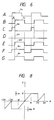
- Phase difference signals ⁇ v and ⁇ r from output terminals Q of the D flip-flops 11 and 12 are applied to two inputs of the NAND gate 13, the output of which is fed to clear terminals CLR of the D flip-flops 11 and 12. Consequently, when the output terminals Q of the D flip-flops 11 and 12 both go to H-logic, the D flip-flops 11 and 12 are cleared and the output terminals Q both return to the L-logic state.
- the D flip-flop 15 forming the lagging signal detector reads therein the L-logic output from the flip-flop 11. Consequently, in this case, the D flip-flop 15 forming the lagging signal detector outputs the H-logic level at the output terminal Q , and hence the AND gate 17B is enabled, through which the input signal fv is output as an appendage pulse Afv to be generated.
- the extended phase difference signal ⁇ v When the extended phase difference signal ⁇ v is H-logic, the potential at a connection point P1 is higher than the virtual grounding potential at the connection point CP, so that the switching diode D3 is turned OFF and the switching diode D1 ON. Consequently, the constant current i1 flowing across the transistor Q1 is applied, as a current +i PD , to the current-voltage converter 14D.
- the potential at the connection point P1 is a junction voltage of the bias adjusting series-connected diode pair Db1 and hence is lower than the potential at the connection point CP, tuning ON the switching diode D3 and OFF the switching diode D1.
- the switching diodes D1 and D2 are simultaneously turned ON and the input currents +i PD and -i PD cancel each other and become zero, with the result that the constant current i1 in the transistor Q1 flows into the transistor Q2. That is, the output voltage of the current-voltage converter 14D is zero.
- the switching diodes D1 and D2 are simultaneously turned OFF, and also in this instance, the output voltage of the current-voltage converter 14D is zero.
- Figs. 5 and 7 it is also possible to employ a construction in which the NAND gate 13 is used also as the lagging signal detector 15 and the pulse generator 17 is a one-shot multivibrator which outputs pulses of a fixed width.
- Fig. 9 illustrates such a modification of the Fig. 5 embodiment.
- One of the input signals fv and fr rises when the output of the NAND gate 13 is H-logic, and then when the other input signal rises, the NAND gate 13 responds thereto to make its output L-logic. In other words, the rise time point of the lagging one of the input signals is thus detected.
- the one-shot multivibrator 17 outputs an appendage pulse of a width which is, for example, one half the period of the signal fv (equal to the period of the signal fr and longer than the dead zone width ⁇ D).
- the appendage pulse thus generated is applied to the pulse appending circuit 16, wherein it is appended to each of the phase difference signals Av and Ar to form the extended phase difference signals ⁇ v and ⁇ r.
- Figs. 5 and 7 outputs the lagging signal fv or fr detected by the lagging signal detector 15, as the appendage pulse via the gate 17A or 17B, so that when the duty ratios of the signals fv and fr become smaller than 50%, the range over which the phase difference can be detected by the phase difference detector 14 becomes narrower than the above-mentioned range of between - ⁇ and + ⁇ .
- the lagging signal detector 15 and the pulse generator 17 are capable of high-speed operation, the embodiments of Figs. 5 and 7 are suitable for phase detection at high frequencies. In particular, in the Fig.
- the phase difference detector 14 detects the phase difference while cancelling the in-phase components of the signals ⁇ v and ⁇ r by switching the currents i1 and i2 by the diodes D1 through D4, and hence is capable of operating at far higher speed than the phase difference detector 14 in the Fig. 5 embodiment.
- the present invention employs the construction in which the phase difference signals Av and Ar are each appended with an appendage pulse of a width larger than the width of the dead zone of the phase difference detector 14 and then are applied thereto--this ensures that the extended phase difference signal Afv or Afr of a pulse width larger than the dead zone width is applied to the phase difference detector 14, even if the phase difference ⁇ between the input signals fv and fr approaches zero.
- the peak values of the phase difference signals Av and Ar which are detected in the vicinity of the phase difference ⁇ equal to zero, vary and become small, it is possible to stably perform the phase detection without being affected by such varying peak values of the phase difference signals and eliminate the dead zone of the phase difference detector.
Landscapes
- Engineering & Computer Science (AREA)
- Power Engineering (AREA)
- Manipulation Of Pulses (AREA)
- Stabilization Of Oscillater, Synchronisation, Frequency Synthesizers (AREA)
- Measuring Phase Differences (AREA)
Claims (5)
- Un détecteur de phase comprenant:
le moyen générant des signaux de différence de phase (11, 12) pour générer deux signaux de différence de phase qui montent à un intervalle de temps correspondant à la différence de phase entre deux signaux d'entrée et descendent en même temps;
le moyen de détection de signal déphasé en arrière (15) pour détecter l'arrivée d'un desdits deux signaux d'entrée déphasé en arrière;
le moyen (16, 17) pour former deux signaux de différence de phase étendus, et
le moyens de détection de différence de phase (14) pour détecter la différence entre lesdits deux signaux de différence de phase étendus et pour présenter en sortie une composante basse fréquence de la différence détectée sous la forme d'une tension correspondant à la différence de phase entre lesdits deux signaux,
caractérisés par
le moyen de génération d'impulsion (17) sensible à la sortie détectée dudit signal déphasé en arrière pour générer une impulsion annexe qui monte au point temporel de détection du signal déphasé en arrière et a une largeur d'impulsion plus grande qu'une largeur prédéterminée; et
le moyen associant une impulsion (16) pour associer ladite impulsion annexe à chacun desdits deux signaux de différence de phase pour former lesdits deux signaux de différence de phase étendus. - Le détecteur de phase de la revendication 1 où ledit moyen de détection de signal déphasé en arrière (15) est formé par une bascule D qui est alimentée à sa borne de données par celui desdits deux signaux de différence de phase et sa borne d'entrée d'horloge avec l'autre desdits deux signaux de différence de phase, et où ledit moyen de génération d'impulsions (17) est formé des première et seconde portes ET (17A et 17B) qui sont alimentées à une borne d'entrée avec une sortie non inversée et une sortie inversée de ladite bascule D, respectivement, et aux autres bornes d'entrée avec lesdits deux signaux d'entrée, respectivement, et une porte OU (17C) qui présente en sortie le résultat de l'opération OU sur les sorties desdites première et seconde portes ET en tant que dite impulsion supplémentaire.
- Le détecteur de phase de la revendication 1 où ledit moyen de génération de signaux de différence de phase inclut les première et seconde bascules qui sont fournies à leur bornes d'entrée d'horloge avec lesdits deux signaux d'entrée, respectivement, et répond à la montée desdits signaux d'entrée pour présenter en sortie des niveaux logiques prédéterminés, et le moyen de porte ET (13) qui est fourni à l'une et l'autre entrées avec les sorties desdites première et seconde bascules et génère un signal de commande pour mettre lesdites première et seconde bascules à leur état initial lorsque leurs sorties sont toutes les deux desdits niveaux logiques prédéterminés, où le moyen de détection de signal déphasé en arrière est utilisé également comme dit moyen de porte ET, et où ledit moyen de génération d'impulsions (17) est un multivibrateur monostable qui répond audit signal de commande provenant dudit moyen de porte ET pour générer ladite impulsion annexe d'une largeur fixée plus importante que ladite largeur prédéterminée.
- Le détecteur de phase de revendication 1 où ledit moyen de détection de différence de phase inclut:
des premier et second moyens de circuits à courant constant (Q₁, Q₂) pour fournir des courants constants de polarités inverses;
des première et seconde diodes de commutation (D₁, D₂) ayant leur anode connectée à la sortie dudit premier moyen de circuit à courant constant (Q₁);
des troisième et quatrième diodes de commutation (D₁, D₂) ayant leur cathode connectée à la sortie dudit second moyen de circuit à courant constant (Q₂), la cathode de ladite première diode de commutation étant connectée à l'anode de ladite troisième diode de commutation;
du moyen de conversion courant-tension (14D) connecté au point de connexion desdites première et troisième diodes de commutation, pour convertir un courant d'entrée passant par celles-ci en la tension correspondante;
du moyen de filtre passe-bas (C, R) pour faire la moyenne de la tension de sortie dudit moyen de conversion courant-tension et pour la présenter en sortie comme une tension correspondant à la différence de phase entre lesdits deux signaux d'entrée;
du premier moyen de contrôle de polarisation (Db₁) pour fournir une polarisation de contrôle à la cathode de ladite seconde diode de commutation (D₃) de sorte que lorsqu'un desdits deux signaux de différence de phase étendus provenant dudit moyen associant une impulsion a l'un des niveaux logiques, lesdites première et seconde diodes de commutation sont rendues passante et bloquée, respectivement, et lorsqu'un desdits signaux de différence de phase étendus a l'autre niveau logique, lesdites première et seconde diodes de commutation sont rendues bloquée et passante, respectivement; et
du second moyen de contrôle de la polarisation (14E, Db₂), pour fournir une polarisation de contrôle à l'anode de ladite quatrième diode de commutation (D₄) de sorte que lorsque l'autre desdits deux signaux de différence de phase étendus provenant dudit moyen associant une impulsion a l'un des niveaux logiques, lesdites troisième et quatrième diodes de commutation sont rendues passante et bloquée, respectivement, lorsque ledit autre signal de différence de phase étendu a l'autre niveau logique, lesdites troisième et quatrième diodes de commutation sont rendues bloquée et passante, respectivement. - Le détecteur de phase de la revendication 3 ou 4 où ladite largeur prédéterminée est la largeur de la zone aveugle dudit moyen de détection de différence de phase (14).
Applications Claiming Priority (2)
| Application Number | Priority Date | Filing Date | Title |
|---|---|---|---|
| JP23449/91 | 1991-02-18 | ||
| JP3023449A JPH04262618A (ja) | 1991-02-18 | 1991-02-18 | 位相検波器 |
Publications (3)
| Publication Number | Publication Date |
|---|---|
| EP0500014A2 EP0500014A2 (fr) | 1992-08-26 |
| EP0500014A3 EP0500014A3 (fr) | 1992-12-30 |
| EP0500014B1 true EP0500014B1 (fr) | 1994-06-15 |
Family
ID=12110815
Family Applications (1)
| Application Number | Title | Priority Date | Filing Date |
|---|---|---|---|
| EP92102607A Expired - Lifetime EP0500014B1 (fr) | 1991-02-18 | 1992-02-17 | Détecteur de phase |
Country Status (4)
| Country | Link |
|---|---|
| US (1) | US5266851A (fr) |
| EP (1) | EP0500014B1 (fr) |
| JP (1) | JPH04262618A (fr) |
| DE (1) | DE69200189T2 (fr) |
Cited By (2)
| Publication number | Priority date | Publication date | Assignee | Title |
|---|---|---|---|---|
| US6329847B1 (en) | 1998-09-29 | 2001-12-11 | U.S. Phillips Corporation | Radio device including a frequency synthesizer and phase discriminator for such a device |
| EP1410510A4 (fr) * | 2001-03-09 | 2004-07-14 | Ericsson Inc | Compensation de glissement de cycle par boucle a phase asservie |
Families Citing this family (32)
| Publication number | Priority date | Publication date | Assignee | Title |
|---|---|---|---|---|
| US5302916A (en) * | 1992-12-21 | 1994-04-12 | At&T Bell Laboratories | Wide range digital frequency detector |
| US5493242A (en) * | 1993-06-30 | 1996-02-20 | Vlsi Technology, Inc. | Status register with asynchronous read and reset and method for providing same |
| US5422918A (en) * | 1993-12-09 | 1995-06-06 | Unisys Corporation | Clock phase detecting system for detecting the phase difference between two clock phases regardless of which of the two clock phases leads the other |
| EP0665650A1 (fr) * | 1994-01-31 | 1995-08-02 | STMicroelectronics S.A. | Détecteur de phase à tension faible, à grande vitesse |
| KR960006292A (ko) * | 1994-07-28 | 1996-02-23 | 사또 겐이찌로 | 주파수위상비교기 |
| JPH08139595A (ja) * | 1994-11-11 | 1996-05-31 | Mitsubishi Electric Corp | 位相比較回路 |
| US5684805A (en) * | 1995-11-30 | 1997-11-04 | Brown; Anthony Kevin Dale | Microwave multiphase detector |
| JPH09251651A (ja) * | 1996-03-15 | 1997-09-22 | Toshiba Corp | 位相差電圧生成回路 |
| US5703502A (en) * | 1996-05-30 | 1997-12-30 | Sun Microsystems, Inc. | Circuitry that detects a phase difference between a first, base, clock and a second, derivative, clock derived from the base clock |
| US6002282A (en) * | 1996-12-16 | 1999-12-14 | Xilinx, Inc. | Feedback apparatus for adjusting clock delay |
| US5977801A (en) * | 1997-07-07 | 1999-11-02 | International Business Machines Corporation | Self-resetting phase/frequency detector with reduced dead zone |
| US5936430A (en) * | 1997-07-21 | 1999-08-10 | Hewlett-Packard Company | Phase detection apparatus and method |
| ATE232317T1 (de) * | 1997-10-10 | 2003-02-15 | Rambus Inc | Verfahren und vorrichtung zur ausfallsicheren resynchronisation mit minimaler latenzzeit |
| US6429694B1 (en) * | 1998-03-02 | 2002-08-06 | International Business Machines Corporation | Apparatus and method in an integrated circuit for delay line phase difference amplification |
| US6064235A (en) * | 1998-03-18 | 2000-05-16 | International Business Machines Corporation | Shared path phase detector |
| US6407599B1 (en) | 2000-05-10 | 2002-06-18 | Eastman Kodak Company | Method and apparatus for determining a digital phase shift in a signal |
| US6868135B1 (en) | 2000-05-18 | 2005-03-15 | Eastman Kodak Company | Method and apparatus for correcting for a phase shift between a transmitter and a receiver |
| US20020109527A1 (en) * | 2000-06-02 | 2002-08-15 | Enam Syed K. | High-speed output driver |
| US6304115B1 (en) * | 2000-07-19 | 2001-10-16 | Marconi Communications, Inc. | Phase locked loop having DC bias circuitry |
| US6778026B2 (en) * | 2002-01-15 | 2004-08-17 | Microtune (San Diego), Inc. | High-speed phase frequency detection module |
| WO2004004126A1 (fr) | 2002-06-28 | 2004-01-08 | Advanced Micro Devices, Inc. | Boucle asservie en phase a syntonisation de frequence automatique |
| US6729994B1 (en) * | 2002-10-29 | 2004-05-04 | General Motors Corporation | Multi-speed transmission mechanisms with three planetary gearsets and clutch input |
| US7461314B2 (en) * | 2003-06-06 | 2008-12-02 | Advantest Corporation | Test device |
| GB2426879C (en) * | 2003-12-12 | 2008-01-21 | Qualcomm Inc | A phase locked loop that sets gain automatically |
| US7038497B2 (en) * | 2004-04-28 | 2006-05-02 | Seiko Epson Corporation | Differential current mode phase/frequency detector circuit |
| US20060017471A1 (en) * | 2004-07-20 | 2006-01-26 | Exar Corporation | Phase detector |
| US7411426B2 (en) * | 2004-07-20 | 2008-08-12 | Exar Corporation | Phase detector for RZ |
| JP4575816B2 (ja) * | 2005-03-23 | 2010-11-04 | 株式会社アドバンテスト | 基準信号に基づいて信号を発生させる発振装置 |
| US8585050B2 (en) | 2011-12-06 | 2013-11-19 | Eastman Kodak Company | Combined ultrasonic-based multifeed detection system and sound-based damage detection system |
| US9285206B1 (en) | 2012-02-07 | 2016-03-15 | Pile Dynamics, Inc. | Measurement device for pile displacement and method for use of the same |
| US20170363667A1 (en) * | 2014-12-19 | 2017-12-21 | Leonardo Mw Ltd | Digital phase meter and phase detection method |
| US9831766B2 (en) * | 2015-11-19 | 2017-11-28 | Mediatek Inc. | Charge pump and associated phase-locked loop and clock and data recovery |
Family Cites Families (9)
| Publication number | Priority date | Publication date | Assignee | Title |
|---|---|---|---|---|
| US4246497A (en) * | 1978-09-29 | 1981-01-20 | Neil Brown Instruments Systems, Inc. | Phase measuring circuit |
| US4264866A (en) * | 1979-01-04 | 1981-04-28 | Ladislav Benes | Frequency and phase comparator |
| US4308500A (en) * | 1979-12-14 | 1981-12-29 | Rca Corporation | Incremental encoder for measuring positions of objects such as rotating shafts |
| US4337435A (en) * | 1980-06-10 | 1982-06-29 | Westinghouse Electric Corp. | Digital phase sequence detector |
| US4378509A (en) * | 1980-07-10 | 1983-03-29 | Motorola, Inc. | Linearized digital phase and frequency detector |
| US4712060A (en) * | 1986-08-29 | 1987-12-08 | Board Of Regents The University Of Texas System | Sampling average phase meter |
| US4901026A (en) * | 1987-07-01 | 1990-02-13 | Rockwell International Corporation | Phase detector circuit having latched output characteristic |
| US4987387A (en) * | 1989-09-08 | 1991-01-22 | Delco Electronics Corporation | Phase locked loop circuit with digital control |
| JPH0736515B2 (ja) * | 1989-09-14 | 1995-04-19 | 株式会社東芝 | 位相比較器 |
-
1991
- 1991-02-18 JP JP3023449A patent/JPH04262618A/ja active Pending
-
1992
- 1992-02-17 EP EP92102607A patent/EP0500014B1/fr not_active Expired - Lifetime
- 1992-02-17 DE DE69200189T patent/DE69200189T2/de not_active Expired - Fee Related
- 1992-02-18 US US07/837,206 patent/US5266851A/en not_active Expired - Fee Related
Cited By (2)
| Publication number | Priority date | Publication date | Assignee | Title |
|---|---|---|---|---|
| US6329847B1 (en) | 1998-09-29 | 2001-12-11 | U.S. Phillips Corporation | Radio device including a frequency synthesizer and phase discriminator for such a device |
| EP1410510A4 (fr) * | 2001-03-09 | 2004-07-14 | Ericsson Inc | Compensation de glissement de cycle par boucle a phase asservie |
Also Published As
| Publication number | Publication date |
|---|---|
| US5266851A (en) | 1993-11-30 |
| JPH04262618A (ja) | 1992-09-18 |
| EP0500014A2 (fr) | 1992-08-26 |
| DE69200189D1 (de) | 1994-07-21 |
| DE69200189T2 (de) | 1994-11-17 |
| EP0500014A3 (fr) | 1992-12-30 |
Similar Documents
| Publication | Publication Date | Title |
|---|---|---|
| EP0500014B1 (fr) | Détecteur de phase | |
| US4623851A (en) | Voltage controlled oscillator using flip-flop controlled switching circuits | |
| US4587496A (en) | Fast acquisition phase-lock loop | |
| US4156855A (en) | Phase-locked loop with variable gain and bandwidth | |
| US7915963B2 (en) | Current controlled oscillation device and method having wide frequency range | |
| US5525932A (en) | Lock indicator for phase locked loop circuit | |
| US20030090327A1 (en) | High-speed and high-precision phase locked loop | |
| US5495207A (en) | Differential current controlled oscillator with variable load | |
| US5105169A (en) | Current controlled oscillator including conversion of control voltage to regular and thresholded control currents | |
| US3924202A (en) | Electronic oscillator | |
| US5619161A (en) | Diffrential charge pump with integrated common mode control | |
| KR960001075B1 (ko) | 위상 검출기 | |
| EP0544109B1 (fr) | Détecteur de phase et circuit PLL le comportant | |
| US11742863B2 (en) | Phase-locked loop circuit | |
| JPH06112815A (ja) | 位相ロック・ループにおけるチャージ・ポンプ | |
| US6188285B1 (en) | Phase-locked loop circuit and voltage-controlled oscillator capable of producing oscillations in a plurality of frequency ranges | |
| US6940323B2 (en) | Phase locked loop circuit with an unlock detection circuit and a switch | |
| US6351154B2 (en) | Phase detector | |
| US6194929B1 (en) | Delay locking using multiple control signals | |
| US20030034847A1 (en) | Charge pump | |
| US5513225A (en) | Resistorless phase locked loop circuit employing direct current injection | |
| US4270093A (en) | Apparatus for forcing a phase-lock oscillator to a predetermined frequency when unlocked | |
| KR20010093790A (ko) | 위상 동기 루프 | |
| US5694086A (en) | Precision, analog CMOS one-shot and phase locked loop including the same | |
| WO2005008895A1 (fr) | Circuit a pompe de charge |
Legal Events
| Date | Code | Title | Description |
|---|---|---|---|
| PUAI | Public reference made under article 153(3) epc to a published international application that has entered the european phase |
Free format text: ORIGINAL CODE: 0009012 |
|
| 17P | Request for examination filed |
Effective date: 19920217 |
|
| AK | Designated contracting states |
Kind code of ref document: A2 Designated state(s): DE FR GB |
|
| PUAL | Search report despatched |
Free format text: ORIGINAL CODE: 0009013 |
|
| AK | Designated contracting states |
Kind code of ref document: A3 Designated state(s): DE FR GB |
|
| 17Q | First examination report despatched |
Effective date: 19930513 |
|
| GRAA | (expected) grant |
Free format text: ORIGINAL CODE: 0009210 |
|
| AK | Designated contracting states |
Kind code of ref document: B1 Designated state(s): DE FR GB |
|
| RIN1 | Information on inventor provided before grant (corrected) |
Inventor name: NUKUI, YOSHIHIRO |
|
| REF | Corresponds to: |
Ref document number: 69200189 Country of ref document: DE Date of ref document: 19940721 |
|
| ET | Fr: translation filed | ||
| PLBE | No opposition filed within time limit |
Free format text: ORIGINAL CODE: 0009261 |
|
| STAA | Information on the status of an ep patent application or granted ep patent |
Free format text: STATUS: NO OPPOSITION FILED WITHIN TIME LIMIT |
|
| 26N | No opposition filed | ||
| PG25 | Lapsed in a contracting state [announced via postgrant information from national office to epo] |
Ref country code: FR Effective date: 19951031 |
|
| REG | Reference to a national code |
Ref country code: FR Ref legal event code: ST |
|
| PG25 | Lapsed in a contracting state [announced via postgrant information from national office to epo] |
Ref country code: GB Effective date: 19960217 |
|
| GBPC | Gb: european patent ceased through non-payment of renewal fee |
Effective date: 19960217 |
|
| PGFP | Annual fee paid to national office [announced via postgrant information from national office to epo] |
Ref country code: DE Payment date: 19990225 Year of fee payment: 8 |
|
| PG25 | Lapsed in a contracting state [announced via postgrant information from national office to epo] |
Ref country code: DE Free format text: LAPSE BECAUSE OF NON-PAYMENT OF DUE FEES Effective date: 20001201 |