EP0500263A2 - Procédé pour synchroniser l'horloge de données d'un récepteur - Google Patents
Procédé pour synchroniser l'horloge de données d'un récepteur Download PDFInfo
- Publication number
- EP0500263A2 EP0500263A2 EP92301175A EP92301175A EP0500263A2 EP 0500263 A2 EP0500263 A2 EP 0500263A2 EP 92301175 A EP92301175 A EP 92301175A EP 92301175 A EP92301175 A EP 92301175A EP 0500263 A2 EP0500263 A2 EP 0500263A2
- Authority
- EP
- European Patent Office
- Prior art keywords
- data
- edge
- phase locked
- locked loop
- clock
- Prior art date
- Legal status (The legal status is an assumption and is not a legal conclusion. Google has not performed a legal analysis and makes no representation as to the accuracy of the status listed.)
- Withdrawn
Links
Images


Classifications
-
- H—ELECTRICITY
- H03—ELECTRONIC CIRCUITRY
- H03L—AUTOMATIC CONTROL, STARTING, SYNCHRONISATION OR STABILISATION OF GENERATORS OF ELECTRONIC OSCILLATIONS OR PULSES
- H03L7/00—Automatic control of frequency or phase; Synchronisation
- H03L7/06—Automatic control of frequency or phase; Synchronisation using a reference signal applied to a frequency- or phase-locked loop
- H03L7/07—Automatic control of frequency or phase; Synchronisation using a reference signal applied to a frequency- or phase-locked loop using several loops, e.g. for redundant clock signal generation
-
- H—ELECTRICITY
- H03—ELECTRONIC CIRCUITRY
- H03L—AUTOMATIC CONTROL, STARTING, SYNCHRONISATION OR STABILISATION OF GENERATORS OF ELECTRONIC OSCILLATIONS OR PULSES
- H03L7/00—Automatic control of frequency or phase; Synchronisation
- H03L7/06—Automatic control of frequency or phase; Synchronisation using a reference signal applied to a frequency- or phase-locked loop
- H03L7/08—Details of the phase-locked loop
- H03L7/099—Details of the phase-locked loop concerning mainly the controlled oscillator of the loop
- H03L7/0991—Details of the phase-locked loop concerning mainly the controlled oscillator of the loop the oscillator being a digital oscillator, e.g. composed of a fixed oscillator followed by a variable frequency divider
- H03L7/0992—Details of the phase-locked loop concerning mainly the controlled oscillator of the loop the oscillator being a digital oscillator, e.g. composed of a fixed oscillator followed by a variable frequency divider comprising a counter or a frequency divider
-
- H—ELECTRICITY
- H03—ELECTRONIC CIRCUITRY
- H03M—CODING; DECODING; CODE CONVERSION IN GENERAL
- H03M5/00—Conversion of the form of the representation of individual digits
- H03M5/02—Conversion to or from representation by pulses
- H03M5/04—Conversion to or from representation by pulses the pulses having two levels
- H03M5/06—Code representation, e.g. transition, for a given bit cell depending only on the information in that bit cell
- H03M5/12—Biphase level code, e.g. split phase code, Manchester code; Biphase space or mark code, e.g. double frequency code
-
- H—ELECTRICITY
- H04—ELECTRIC COMMUNICATION TECHNIQUE
- H04L—TRANSMISSION OF DIGITAL INFORMATION, e.g. TELEGRAPHIC COMMUNICATION
- H04L25/00—Baseband systems
- H04L25/38—Synchronous or start-stop systems, e.g. for Baudot code
- H04L25/40—Transmitting circuits; Receiving circuits
- H04L25/49—Transmitting circuits; Receiving circuits using code conversion at the transmitter; using predistortion; using insertion of idle bits for obtaining a desired frequency spectrum; using three or more amplitude levels ; Baseband coding techniques specific to data transmission systems
- H04L25/4904—Transmitting circuits; Receiving circuits using code conversion at the transmitter; using predistortion; using insertion of idle bits for obtaining a desired frequency spectrum; using three or more amplitude levels ; Baseband coding techniques specific to data transmission systems using self-synchronising codes, e.g. split-phase codes
-
- H—ELECTRICITY
- H04—ELECTRIC COMMUNICATION TECHNIQUE
- H04L—TRANSMISSION OF DIGITAL INFORMATION, e.g. TELEGRAPHIC COMMUNICATION
- H04L7/00—Arrangements for synchronising receiver with transmitter
- H04L7/02—Speed or phase control by the received code signals, the signals containing no special synchronisation information
- H04L7/033—Speed or phase control by the received code signals, the signals containing no special synchronisation information using the transitions of the received signal to control the phase of the synchronising-signal-generating means, e.g. using a phase-locked loop
- H04L7/0334—Processing of samples having at least three levels, e.g. soft decisions
-
- H—ELECTRICITY
- H04—ELECTRIC COMMUNICATION TECHNIQUE
- H04L—TRANSMISSION OF DIGITAL INFORMATION, e.g. TELEGRAPHIC COMMUNICATION
- H04L7/00—Arrangements for synchronising receiver with transmitter
- H04L7/04—Speed or phase control by synchronisation signals
- H04L7/041—Speed or phase control by synchronisation signals using special codes as synchronising signal
- H04L7/046—Speed or phase control by synchronisation signals using special codes as synchronising signal using a dotting sequence
Definitions
- This invention relates to a receiving apparatus and a method therefor for synchronising a digital data clock in a receiver with a digital data clock in a transmitter.
- each data bit has one of two values which are represented by high and low voltage levels on the cable, the low voltage levels being represented by data level "0" and the high voltage levels being represented by data level "1".
- NZ no return to zero
- a preamble of alternating 0's and 1's is transmitted and such a preamble waveform for the NRZ data is shown in Figure 2(a) and for the Manchester encoded data is shown in Figure 2(b).
- the Manchester encoded data preamble waveform as shown in Figure 2(b), only has transitions in the middle of every bit period and not at the end of the bit periods, and it is a square wave at exactly half the frequency of the transmitted NRZ data rate shown in Figure 2(a).
- the receiver is, thus, able to use the preamble to synchronise its own clock and the ensuing transition in the middle of every bit period is used to maintain the synchronisation.
- a digital phase-locked loop requires no such precision components. However, its resolution is very much limited by its sampling frequency. Therefore, to take the example of ETHERNET, if it was decided that a clock accuracy of ⁇ 5ns was required, this would require a 200MHz sampling rate in a conventional digital phase locked loop. This is above the maximum clock frequency achievable in most current silicon technologies.
- a receiving apparatus for synchronising a digital data clock in a receiver with a digital data clock in a transmitter, said receiver being adapted to receive encoded data formed by a plurality of bits, each said bit having a predetermined period, said receiver including means for detecting positive and negative going edges of said encoded data and to provide positive and negative edge detection signals indicative thereof, a first phase locked loop adapted to receive said positive edge detection signals, a second phase locked loop adapted to receive said negative edge detection signals, said first and second phase locked loops including means for determining whether an edge is in substantially the middle of a bit period indicative of a data edge or an edge at the end of a bit period indicative of a non-data edge, and clock and data recovery means connected to receive output signals from said first and second phase locked loops, said recovery means being adapted to reproduce said transmitted data bits in dependence upon the outputs from the first and second phase locked loops, whereby an output from said first phase locked loop indicates to said recovery means a logical "1" was transmitted and an
- a method of synchronising a digital data clock in a receiver with a digital data clock in a transmitter said receiver being adapted to receive encoded data formed by a plurality of bits, each said bit having a predetermined period, said receiver operation including the steps of detecting positive and negative going edges of the received encoded data and providing positive and negative edge detection signals indicative thereof, receiving said positive edge detection signals in a first phase locked loop, receiving said negative edge detection signals in a second phase locked loop, said first and second phase locked loops determining whether an edge is in substantially the middle of a bit period indicative of a data edge or an edge at the end of a bit period indicative of a non-data edge, and recovering output signals from said first and second phase locked loops to reproduce said transmitted data bits in dependence upon the outputs of each of the first and second phase locked loops whereby an output from said first phase locked loop indicates a logical "1" was transmitted and an output from said second phase locked loop indicates a logical "0" was transmitted.
- said received data comprises encoded data with a period of one half the bit period of transmitted data and an expected data edge at approximately the middle of each transmitted data period and each phase locked loop has a counter means for maintaining lock on said data such that when a data or a non-data edge occurs the phase locked loop compares the actual edge position with the expected position of the edge and if the edge is later than expected the counter associated with said phase locked loop is incremented and if the edge is earlier than expected the counter associated with said phase locked loop is decremented.
- the sampling period where data and non-data edges are expected is advanced or retarded respectively by one sample.
- a disable signal is sent to the other of said first and second phase locked loops to prevent said other of said first and second phase locked loops detecting a data edge.
- the received encoded data includes a preamble portion of data bits and, advantageously, the first and second phase locked loops are arranged to ignore a first predetermined number of bits of said preamble portion, said predetermined number of bits being dependent upon when the received signal jitter is substantially constant.
- the preamble portion of data bits of the received data is such that every edge is a data edge and means are provided for sampling each said bit at a predetermined rate after detecting said data edge.
- the number of samples n is four or a multiple thereof, and at sampling periods n/4 and 3n/4 if an edge is detected as a data edge by one of the first and second phase locked loops then a data valid signal is sent from the detecting phase locked loop to the clock and data recovery means but no change is made to the count of the detecting phase locked loop counter means, and a data disable signal is transmitted from the detecting phase locked loop to the other phase locked loop for preventing said other phase locked loop from generating a data valid signal for a predetermined number of sampling periods.
- the clock and data recovery means recovers the data signal using a set/reset arrangement in which the data valid signal from the positive edge triggered phase locked loop sets the decoded data signal and the data valid signal from the negative edge triggered phase locked loop resets the decoded data signal whereby NRZ received data is produced. Additionally, advantageously, the clock and data recovery means recovers the clock data by detecting whenever one of the data valid signals becomes active, whereby the clock signal is set active at a predetermined time after the change in the NRZ data and thereafter the clock signal is set inactive ready for the next time one of the data valid signals goes active, whereby the active edges in the clock signal are used to sample the decoded data.
- the apparatus and method of this invention is designed to be operable in particular with Manchester encoded data.
- the receiving apparatus for synchronising a digital data clock signal in a receiver is shown in simplified block schematic form in Figure 3 and has a noise rejection circuit 1 adapted to receive transmitted Manchester encoded data, on a receive data input 2, and a clock terminal 3 with which to sample, i.e. digitize, the data.
- the receive data is sampled to produce two signals, one of which indicates that a positive edge was detected in the sampling period (positive edge data detect) which is output on line 4 and the other to indicate that a negative edge was detected (negative edge data detect) which is output on line 5, the line 4 being connected to a positive edge triggered phase-locked loop 6 and the line 5 being connected to a negative edge triggered phase-locked loop 7.
- the noise rejection circuit is also arranged to detect when valid data is present on the receive data input line and controls the enabling and disabling of the phase-locked loops 6 and 7 via an enable/disenable line 8.
- a fast lock circuit is employed which ensures that it can quickly lock onto an incoming waveform.
- the present invention makes use of the fact that, after the first few bits of preamble in the receive waveform, the position of the edges in the waveform will have stabilised and the jitter will be substantially constant.
- the noise reject circuit 1 if enabling of the phase-locked loops is delayed until a fixed number of bits after a valid receive waveform has been detected by the noise reject circuit 1, the phase-locked loops 6, 7 will lock onto a stable waveform and so have no need for a fast lock circuit.
- the implementation of a fast lock circuit which may be used with the phase-locked loops of this invention will be described later herein.
- phase-locked loops 6, 7 each receive two signals from the noise reject circuit 1, a phase-locked loop enable signal supplied over line 8 which is common to both of the phase-locked loops and either a positive or negative edge detect signal over line 4 or 5 respectively.
- a phase-locked loop enable signal supplied over line 8 which is common to both of the phase-locked loops and either a positive or negative edge detect signal over line 4 or 5 respectively.
- phase-locked loop If a phase-locked loop has been disabled and is then enabled, it will remain in the idle state until its edge detect signal goes active and will then make the assumption that this edge represents the correct sampling period in which to detect a data edge.
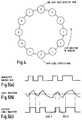
- the activated phase-locked loop will then begin to rotate around a sampling loop, as shown in Figure 4, in which the bit period is split into a number of sampling periods, denoted by numbers 0 to 11. Although the example shown in Figure 4 has the bit periods split into twelve sampling periods, the actual number will depend upon the relationship between the bit period and the sampling frequency, although the phase-locked loops will usually have an even number of samples in one bit period.
- a data valid signal is sent from the detecting phase-locked loop to a clock and data recovery circuit 9, whereby a data level "1" detected by phase-locked loop 6 is transmitted to circuit 9 over line 10 and a data level "0" is transmitted to the circuit 9 over line 11.
- the sample period in which the first edge is seen is numbered 0 and the phase-locked loop performing the sampling will expect to see data edges in sample 0 and non-data edges in sample 6. If an edge occurs in sample 1, the phase-locked loop would assume that this was a data edge, but shifted backwards by one sampling period from its nominal position. The phase-locked loop data detect line will then go active to indicate to the clock and data recovery circuit 9 that a data edge has occurred and the phase-locked loop counter will be incremented to record that the data edge was after its expected position. Similarly, an edge in sample 2 will be interpreted as a data edge but shifted further from its expected position and the data detect line will go active and the counter will be incremented. The value by which the counter is incremented may be the same as for an edge in sample 1 or, advantageously, could be larger to reflect the fact that the edge was further from its expected position.
- Non-data edges are treated in exactly the same manner, with the counter being incremented for edges ahead of their expected position, e.g. samples 7 and 8, and decremented for those lagging their expected position, e.g. samples 4 and 5. However, any non-data edges detected will not set the data detect line active.
- the counter value will eventually reach a minimum or maximum value in dependence upon the difference in frequency between the transmit clock and the receiver sampling clock. Once this value is reached then the sampling periods in which data and non-data edges are expected will be either advanced or retarded by one sampling period, thus maintaining lock on the incoming data waveform.
- the counter is also reset back to its intermediate (usually median) value and the whole process repeats. The positive and negative edged triggered phase-locked loops will continue to maintain lock in this fashion until the noise reject circuit 9 detects the end of the data packet that has been received and disables the phase-locked loops.
- the circuit 9 thus provides clock pulses for sampling the synchronised data to terminal 12 and synchronised data to terminal 13.
- the counter is reset to a median value, so as to more closely simulate an analogue phase-locked loop, the counter may be set to a value close to the limit opposite the one which caused the counter to be reset, that is if the counter has reached its predefined maximum value then it should be reset to a value close to the minimum counter value.
- Such resetting is so that the counter value gives a representation of the nominal edge position within a sample period and so the counter being reset close to the opposite limit indicates the nominal edge position that has just crossed a sampling period boundary.
- the transmitted waveform of Manchester encoded data shown in Figure 5(a) when applied to the interconnecting cable between transmitter and receiver, adopts the waveform shown in Figure 5(b) in which the top broken line denotes logic threshold level "1" and the bottom broken line denotes logic threshold level "0".
- the waveform of Figure 5(c) denotes the digitized cable waveform in which the nominal edge positions are shown by broken lines. From the waveforms of Figures 5(a) - 5(c) it can be seen that jitter has been introduced to the edges of the received waveform ( Figure 5(c)).
- any edge in one of the two unused sampling periods 3 and 9 in Figure 4 is detected as a data edge and sets the data detect signal but then makes no change to the phase-locked loop count.
- the detecting phase-locked loop sends out a data disable signal over line 14 or 15 in dependence upon which of the phase-locked loops detect the data edge, to prevent the non-detecting phase-locked loop from generating a data valid signal for a predetermined number of periods, for example two sampling periods.
- both edges may have occurred in the unused sampling period, only the first edge will generate a valid data signal to the clock and data recovery circuit 9.
- each phase-locked loop consists of two loops with the expected edge position of the data separated by half a system clock.
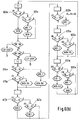
- Figures 6(a) and 6(b) show the state machine diagram for one of the phase-locked loops, the representation shown in Figure 6(a) showing the situation occurring when the expected data edge position is in the second half of the sampling clock period and the state machine diagram of Figure 6(b) showing the situation occurring when the expected data edge position occurs in the first half of the sample clock period.
- the phase-locked loop begins in the idle state 601 and the first edge to occur is assumed to represent the correct sampling period for data edges and the phase-locked loop begins to start rotating around one of the two loops represented by Figures 6(a) and 6(b).
- Edges are processed as shown in the diagrams whereby, from step 601, at step 602 the counter is reset to its intermediate (normally median) value whenever the phase-locked loop is idle or it is switching between loops.
- Position 603 is a decision box representative of sampling period 0 of Figure 4 and is indicative of a data edge occurring in the second half of the sampling clock period. If an edge is present in the second half of the previous clock cycle then a high level "1" output is applied to data detect line active box 604. If no edge is detected at step 603 then the absence or presence of a data edge is detected at the first half of the sample clock period, as indicated by step 605, the step 605 also occurring in the sampling period 0 of Figure 4. If no edge is detected at step 605 then the state reverts to the idling step 601. If an edge is present at step 605 then output is provided to the data detect line active box 606 and the sequence moves to position S3 shown in Figure 6(b).
- step S4 Output from boxes 613 and 616, and the absence of an edge in sample 2 (614), moves the sequence to step S4 and sample period 4 is reviewed. If an edge is detected in sample 4 (box 617) then the count of the counter is subtracted by 2 at step 618 then the sequence moves to step S6. If no edge is detected the sample period 4 then it is determined if an edge is present in the third sample period (619) and if no edge is detected then the procedure steps to step S6, but if an edge is present then at step 620 a data disable signal is applied to the other phase-locked loop.
- step S6 it is determined whether in the sample period 5 (box 621) whether or not an edge is present in the second half of the sample period 5 of Figure 4. If an edge is present then a 1 is subtracted from the counter at step 622, but if an edge is not present then the sequence moves to step S8.
- the sample period 6 of Figure 4 is not present in the diagram of Figure 6(a) (or Figure 6(b)) since this sample period is where non-data edges are expected, but if sample periods other than 12 are taken then the detection of edges in the first half of the sample period 6 would be made if the output from box 621 were not active.
- step S8 the sample period 7 of Figure 4 is reviewed and if an edge is detected in sample period 7 (denoted by box 623) then a 1 is added at step 624 to the counter and the sequence moves to step S10. If, however, no edge is detected at step 623 then the sequence moves to consider whether a data edge is present in sample period 8 of Figure 4, which is denoted by box 625 in Figure 6(a). If no edge is detected at step 625 then the sequence moves to step S10, but if an edge is detected then a 2 is added to the count of the counter at step 626.
- step S10 the tenth sample is reviewed to determine if an edge is present (box 627) and if such an edge is present then a 2 is subtracted from the count of the counter at step 628 and a data disable signal is sent at step 629 to the other phase-locked loop. If no data edge is detected at step 627 then it is determined whether an edge is present in the sample period 9, as denoted by the box 630. If a data edge is detected then a data disable signal is transmitted to the other phase-locked loop at step 631, but if an edge is not present then, similarly with the outputs of boxes 629 and 631, the sequence returns to step S0.
- step S0 it is determined whether the sample period 0 (denoted by box 603') has an edge present which will inherently be a data edge and if it has then the sequence moves to the data detect line active box 604, but if no edge is present then it is determined if an edge is present in sample period 11 (box 632). If no edge is present then the sequence moves to step 607, but if an edge is present then the count of the counter is subtracted by 1 (step 633) whereupon the data detect line is made active at step 634 and the sequence, again, moves to step 607.
- CLR.COUNT causes the counter to be reset to its intermediate value whenever the phase-locked loop is idle or it is switching between loops and the DATA.
- DIS block means that both data detect line 14, 15 and the disable data line to the other phase-locked loop are set active for the next two generating periods to prevent it from generating a data detect output, all of these conditions being as described above in relation to Figure 6(a).
- the clock and data recovery circuit detects data high (1) and data low (0) signals from the phase-locked loops and uses them to regenerate the transmitted data in NRZ format and a clock with which the data can be sampled.
- the data signal is recovered using a set/reset arrangement in which the data valid signal from the positive edge triggered phase-locked loop sets the decoded data signal and the same signal from the negative edge triggered phase-locked loop resets the decoded data signal. Such an arrangement, therefore, provides the required NRZ received data.
- the clock is recovered by detecting whenever one of the data valid signals has gone active. When this occurs the clock signal is set active some time after the change in the NRZ data so as to provide a data setup time before the clock goes active, for example to a logic 1. The clock signal is then set inactive, ready for the next time one of the data valid signals goes active. The active edges in the clock can then be used to sample the decoded data.
- a fast lock circuit may be implemented if the above noted method of ignoring a portion of the preamble was not suitable. Because in the preamble sequence of alternating 1's and 0's, every edge is a data edge (see Figures 2(a) and 2(b)) then data edges can be detected in every sample period within each bit except sample 6 where no decision can be made since it is equidistant from the expected edge position 0. Thus, the danger of a large amount of variation in the position of the first few edges in the received waveform causing the data edges to move outside of the set of sample periods in which they will be detected is eliminated, provided their position does not shift by more than half a period of the received data.
Landscapes
- Engineering & Computer Science (AREA)
- Computer Networks & Wireless Communication (AREA)
- Signal Processing (AREA)
- Theoretical Computer Science (AREA)
- Physics & Mathematics (AREA)
- Spectroscopy & Molecular Physics (AREA)
- Synchronisation In Digital Transmission Systems (AREA)
Applications Claiming Priority (3)
| Application Number | Priority Date | Filing Date | Title |
|---|---|---|---|
| GB919103562A GB9103562D0 (en) | 1991-02-20 | 1991-02-20 | Apparatus and method for synchronising a digital data clock in a receiver with a digital data clock in a transmitter |
| GB9103562 | 1991-02-20 | ||
| US07/858,344 US5297869A (en) | 1991-02-20 | 1992-03-26 | Apparatus and method for synchronizing a digital data clock in a receiver with a digital data clock in a transmitter |
Publications (2)
| Publication Number | Publication Date |
|---|---|
| EP0500263A2 true EP0500263A2 (fr) | 1992-08-26 |
| EP0500263A3 EP0500263A3 (en) | 1993-06-09 |
Family
ID=26298467
Family Applications (1)
| Application Number | Title | Priority Date | Filing Date |
|---|---|---|---|
| EP19920301175 Withdrawn EP0500263A3 (en) | 1991-02-20 | 1992-02-13 | Method for synchronising a receiver's data clock |
Country Status (2)
| Country | Link |
|---|---|
| US (1) | US5297869A (fr) |
| EP (1) | EP0500263A3 (fr) |
Cited By (3)
| Publication number | Priority date | Publication date | Assignee | Title |
|---|---|---|---|---|
| WO1999044327A2 (fr) | 1998-02-26 | 1999-09-02 | Koninklijke Philips Electronics N.V. | Circuit d'extraction d'horloge et recepteur dote d'un tel circuit |
| CN1064491C (zh) * | 1995-12-15 | 2001-04-11 | 章谦 | 一种抗时钟抖动能力强的零次群接口解码方法及其电路 |
| CN102347813A (zh) * | 2011-09-26 | 2012-02-08 | 华为技术有限公司 | 一种选取采样时钟信号的方法和设备 |
Families Citing this family (18)
| Publication number | Priority date | Publication date | Assignee | Title |
|---|---|---|---|---|
| JP3084151B2 (ja) * | 1992-09-18 | 2000-09-04 | 株式会社日立製作所 | 情報処理システム |
| SG74622A1 (en) * | 1998-03-31 | 2000-08-22 | Motorola Inc | Clock recovery circuit |
| FR2778044B1 (fr) * | 1998-04-23 | 2000-06-16 | Thomson Multimedia Sa | Procede de recuperation d'horloge lors de l'echantillonnage des signaux de type informatique |
| KR100318842B1 (ko) * | 1998-11-26 | 2002-04-22 | 윤종용 | 디지털위상제어루프에서의주파수검출방법 |
| JP3657188B2 (ja) | 2000-10-31 | 2005-06-08 | Necエレクトロニクス株式会社 | 装置及びその動作方法 |
| GB0026614D0 (en) * | 2000-10-31 | 2000-12-13 | Lsi Logic Europ Ltd | A method and apparatus for estimation of error in data recovery schemes |
| US6988227B1 (en) * | 2001-06-25 | 2006-01-17 | Silicon Laboratories Inc. | Method and apparatus for bit error rate detection |
| US6856206B1 (en) * | 2001-06-25 | 2005-02-15 | Silicon Laboratories, Inc. | Method and apparatus for acquiring a frequency without a reference clock |
| US6946881B1 (en) * | 2002-06-14 | 2005-09-20 | National Semiconductor Corporation | Method to detect the polarity of sync signals without external capacitor or clock |
| US7085970B2 (en) * | 2002-07-23 | 2006-08-01 | International Business Machines Corporation | Fast detection of incorrect sampling in an oversampling clock and data recovery system |
| US6664859B1 (en) * | 2002-09-13 | 2003-12-16 | Faaday Technology Crop. | State machine based phase-lock-loop for USB clock recovery |
| US7406100B2 (en) * | 2003-05-21 | 2008-07-29 | Atmel Corporation | Bi-directional single wire interface |
| JP3990319B2 (ja) * | 2003-06-09 | 2007-10-10 | 株式会社アドバンテスト | 伝送システム、受信装置、試験装置、及びテストヘッド |
| WO2005013546A1 (fr) * | 2003-07-31 | 2005-02-10 | Advantest Corporation | Unite de transfert de signal d'horloge et equipement de test |
| FR2862820B1 (fr) * | 2003-11-21 | 2006-03-31 | Atmel Nantes Sa | Circuit electronique de decodage d'un signal de donnees asynchrone biphase et procede de decodage correspondant, dispositif de controle d'un equipement |
| US7375591B2 (en) * | 2006-08-04 | 2008-05-20 | Silicon Laboratories Inc. | Robust false locking prevention in referenceless frequency acquisition |
| US20090265490A1 (en) * | 2008-04-04 | 2009-10-22 | Tarun Setya | High-Speed Video Serializer and Deserializer |
| US9875209B2 (en) * | 2013-05-06 | 2018-01-23 | Qualcomm Incorporated | Synchronous data-link throughput enhancement technique based on data signal duty-cycle and phase modulation/demodulation |
Family Cites Families (4)
| Publication number | Priority date | Publication date | Assignee | Title |
|---|---|---|---|---|
| KR900001593B1 (ko) * | 1985-03-30 | 1990-03-15 | 가부시끼가이샤 도오시바 | 디지탈신호 재생회로 |
| EP0262609A3 (fr) * | 1986-09-30 | 1990-04-04 | Siemens Aktiengesellschaft | Boucle numérique de réglage de phase |
| JPH0282835A (ja) * | 1988-09-20 | 1990-03-23 | Sony Corp | ディジタル信号受信装置 |
| US4984255A (en) * | 1989-11-15 | 1991-01-08 | National Semiconductor Corporation | Edge transition insensitive delay line system and method |
-
1992
- 1992-02-13 EP EP19920301175 patent/EP0500263A3/en not_active Withdrawn
- 1992-03-26 US US07/858,344 patent/US5297869A/en not_active Expired - Fee Related
Cited By (5)
| Publication number | Priority date | Publication date | Assignee | Title |
|---|---|---|---|---|
| CN1064491C (zh) * | 1995-12-15 | 2001-04-11 | 章谦 | 一种抗时钟抖动能力强的零次群接口解码方法及其电路 |
| WO1999044327A2 (fr) | 1998-02-26 | 1999-09-02 | Koninklijke Philips Electronics N.V. | Circuit d'extraction d'horloge et recepteur dote d'un tel circuit |
| CN102347813A (zh) * | 2011-09-26 | 2012-02-08 | 华为技术有限公司 | 一种选取采样时钟信号的方法和设备 |
| US9026832B2 (en) | 2011-09-26 | 2015-05-05 | Huawei Technologies Co., Ltd. | Method, system and device for removing media access control addresses |
| CN102347813B (zh) * | 2011-09-26 | 2015-11-25 | 华为技术有限公司 | 一种选取采样时钟信号的方法和设备 |
Also Published As
| Publication number | Publication date |
|---|---|
| US5297869A (en) | 1994-03-29 |
| EP0500263A3 (en) | 1993-06-09 |
Similar Documents
| Publication | Publication Date | Title |
|---|---|---|
| US5297869A (en) | Apparatus and method for synchronizing a digital data clock in a receiver with a digital data clock in a transmitter | |
| US6008746A (en) | Method and apparatus for decoding noisy, intermittent data, such as manchester encoded data or the like | |
| US7466772B2 (en) | Decoding coded data streams | |
| US5278874A (en) | Phase lock loop frequency correction circuit | |
| US6546063B1 (en) | Asynchronous clock for adaptive equalization | |
| US4088832A (en) | Split phase code synchronizer and demodulator | |
| JPH0150150B2 (fr) | ||
| US5717728A (en) | Data/clock recovery circuit | |
| US6396877B1 (en) | Method and apparatus for combining serial data with a clock signal | |
| EP0146609A1 (fr) | Decodeur manchester | |
| US6675326B1 (en) | Method and apparatus for detecting a data receiving error | |
| US6794945B2 (en) | PLL for clock recovery with initialization sequence | |
| US6933866B1 (en) | Variable data rate receiver | |
| US4813058A (en) | FSK signal demodulator | |
| JPH027544B2 (fr) | ||
| US4759040A (en) | Digital synchronizing circuit | |
| US6704382B1 (en) | Self-sweeping autolock PLL | |
| CA1278049C (fr) | Circuit numerique pouvant extraire des signaux de synchronisation d'un flux de donnees codees | |
| US20050060052A1 (en) | Digital audio data receiver without synchronized clock generator | |
| US4760344A (en) | Phase shift keying signal demodulation method and apparatus | |
| WO2009038906A1 (fr) | Détecteur de phase-fréquence avec tolérance à la gigue élevée | |
| US4412302A (en) | Digital phase demodulation and correlation | |
| WO1991004619A1 (fr) | Procede et appareil de recuperation de donnees, telles que des donnees de teletexte codees en signaux de television | |
| US20010028693A1 (en) | Method and circuit for glithch-free changing of clocks having different phases | |
| US7136446B2 (en) | Method and apparatus for data and clock recovery in a biphase-coded data signal |
Legal Events
| Date | Code | Title | Description |
|---|---|---|---|
| PUAI | Public reference made under article 153(3) epc to a published international application that has entered the european phase |
Free format text: ORIGINAL CODE: 0009012 |
|
| AK | Designated contracting states |
Kind code of ref document: A2 Designated state(s): DE FR GB IT NL SE |
|
| PUAL | Search report despatched |
Free format text: ORIGINAL CODE: 0009013 |
|
| AK | Designated contracting states |
Kind code of ref document: A3 Designated state(s): DE FR GB IT NL SE |
|
| 17P | Request for examination filed |
Effective date: 19930727 |
|
| 17Q | First examination report despatched |
Effective date: 19951130 |
|
| GRAH | Despatch of communication of intention to grant a patent |
Free format text: ORIGINAL CODE: EPIDOS IGRA |
|
| 18D | Application deemed to be withdrawn |
Effective date: 19960716 |